US7474129B2 - Dual mode comparator - Google Patents

Dual mode comparator Download PDF

Info

Publication number
US7474129B2
US7474129B2 US11/409,712 US40971206A US7474129B2 US 7474129 B2 US7474129 B2 US 7474129B2 US 40971206 A US40971206 A US 40971206A US 7474129 B2 US7474129 B2 US 7474129B2
Authority
US
United States
Prior art keywords
differential transistor
multiplexor
dual mode
differential
comparator
Prior art date
Legal status (The legal status is an assumption and is not a legal conclusion. Google has not performed a legal analysis and makes no representation as to the accuracy of the status listed.)
Active, expires
Application number
US11/409,712
Other versions
US20060250165A1 (en
Inventor
Brian Carey
Current Assignee (The listed assignees may be inaccurate. Google has not performed a legal analysis and makes no representation or warranty as to the accuracy of the list.)
Analog Devices Inc
Original Assignee
Analog Devices Inc
Priority date (The priority date is an assumption and is not a legal conclusion. Google has not performed a legal analysis and makes no representation as to the accuracy of the date listed.)
Filing date
Publication date
Application filed by Analog Devices Inc filed Critical Analog Devices Inc
Priority to US11/409,712 priority Critical patent/US7474129B2/en
Assigned to ANAALOG DEVICES, INC. reassignment ANAALOG DEVICES, INC. ASSIGNMENT OF ASSIGNORS INTEREST (SEE DOCUMENT FOR DETAILS). Assignors: CAREY, BRIAN
Assigned to ANALOG DEVICES, INC. reassignment ANALOG DEVICES, INC. CORRECTIVE ASSIGNMENT TO CORRECT THE SPELLING OF THE ASSIGNEE'S NAME FROM ANAALOG DEVICES, INC. TO ANALOG DEVICES, INC. PREVIOUSLY RECORDED ON REEL 017789 FRAME 0076. ASSIGNOR(S) HEREBY CONFIRMS THE CORRECT SPELLING OF THE ASSIGNEE'S NAME IS ANALOG DEVICES, INC.. Assignors: CAREY, BRIAN
Publication of US20060250165A1 publication Critical patent/US20060250165A1/en
Application granted granted Critical
Publication of US7474129B2 publication Critical patent/US7474129B2/en
Active legal-status Critical Current
Adjusted expiration legal-status Critical

Links

Images

Classifications

    • HELECTRICITY
    • H03ELECTRONIC CIRCUITRY
    • H03KPULSE TECHNIQUE
    • H03K5/00Manipulating of pulses not covered by one of the other main groups of this subclass
    • H03K5/22Circuits having more than one input and one output for comparing pulses or pulse trains with each other according to input signal characteristics, e.g. slope, integral
    • H03K5/24Circuits having more than one input and one output for comparing pulses or pulse trains with each other according to input signal characteristics, e.g. slope, integral the characteristic being amplitude
    • H03K5/2409Circuits having more than one input and one output for comparing pulses or pulse trains with each other according to input signal characteristics, e.g. slope, integral the characteristic being amplitude using bipolar transistors
    • H03K5/2418Circuits having more than one input and one output for comparing pulses or pulse trains with each other according to input signal characteristics, e.g. slope, integral the characteristic being amplitude using bipolar transistors with at least one differential stage

Definitions

  • the present invention relates to comparators and more specifically to dual mode comparators.
  • Dual mode comparators are often used in automatic testing equipment (ATE) for testing one or more devices under tests (DUTs). Dual mode comparators can operates in any one of a plurality of modes including a differential mode, a common mode, and single-ended mode wherein the mode is selectable based upon an external selection signal provided to the dual mode comparator.
  • ATE automatic testing equipment
  • Dual mode comparators can operates in any one of a plurality of modes including a differential mode, a common mode, and single-ended mode wherein the mode is selectable based upon an external selection signal provided to the dual mode comparator.
  • the prior art designs provide separate circuitry for each of the modes. Additionally, for each comparison, there is a separate normal windowing comparator (NWC) as shown in FIG. 1 .
  • NWC normal windowing comparator
  • FIG. 1 shows two inputs provided into the prior art dual mode comparator circuit, which are labeled DUT 1 101 and DUT 2 102 . These inputs are each coupled to a device under test. These inputs may be attached to two separate inputs from a single device or the inputs may be coupled to two separate devices.
  • the circuit includes a pair of output multiplexors (MUX) 103 , 104 . Each multiplexor receives a control signal that determines the selected comparator mode to output. Thus, by way of example, for the first multiplexor 103 , each NWC 110 , 111 , 112 , 113 is active and produces an output signal.
  • MUX output multiplexors
  • the multiplexor 103 receives in four input signal and selects two of the four input signals to output (either a single ended comparison of DUT 1 with VOH 1 and a single ended comparison of DUT 1 with VOL 1 , or a differential comparison with VOH 1 and a differential comparison with VOL 1 ).
  • each NWC 110 , 111 , 112 , 113 circuit is always active.
  • Each NWC 110 , 111 , 112 , 113 circuit includes at least two stages, a comparison stage and an amplification stage. Therefore, the prior art configuration always requires power for the NWC.
  • a dual mode comparator circuit includes a plurality of differential transistor pairs. Each differential transistor pair includes a plurality of inputs and outputs. The outputs of the differential transistor pairs are coupled to inputs of a multiplexor.
  • the multiplexor includes at least one control input for selecting between the multiplexor inputs and provides the selected input to the multiplexor output.
  • the dual mode comparator further includes a comparator back end that is coupled to the output of the multiplexor.
  • the comparator back end may include a folded cascode and additional gain stages. The comparator back end provides the comparator output to the next stage.
  • the dual mode comparator may be used in automatic testing equipment embodiments wherein both power and space are at a premium.
  • the disclosed dual mode comparator circuit reduces both the required power and reduces the silicon area need to implement the dual mode comparator as compared with the prior art.
  • the differential transistor pairs are formed from a plurality of bipolar transistors. In other embodiments, other transistor types, such as, CMOS transistors may be employed.
  • the bipolar transistors each include an emitter, collector and base. The input for each differential transistor pair is received into the base of the transistors.
  • the multiplexor is coupled to the collector of the bipolar transistors.
  • a current source is provided at the emitters of the differential bipolar transistor pairs. In one embodiment, additional current sources are coupled between the output of the multiplexor and the input of the comparator back end. In other embodiments, additional current sources may be coupled between the differential transistor pairs and the inputs to the multiplexor.
  • the multiplexor will route the differential input signal from the differential transistor pair either to the comparator back end or to a voltage rail.
  • the multiplexor can be formed from a plurality of bipolar transistor pairs where the emitters of an input pair of transistors of the multiplexor are coupled to the collectors of a differential transistor pair and the collectors of an output pair of transistors of the multiplexor are coupled to a comparator back end.
  • Also disclosed is a method for selection of an input signal in a dual mode comparator First, an input signal is compared with another signal (either a reference voltage or another input signal) using a differential transistor pair.
  • the differential transistor pair generates an output based upon the two input signals.
  • a multiplexor is coupled to the output of the differential transistor pair, where a selection signal is received by the multiplexor and the output of the desired differential transistor pair is received by the comparator back end.
  • the comparator back end includes a gain stage that amplifies the desired differential signal.
  • Embodiments of the dual mode comparator reduce the number of gain stages, since a single comparator back end may be shared by a plurality of comparator front ends/differential transistor pairs.
  • the dual mode comparator benefits from operating in the current domain, such that the additional capacitance that occurs due to the additional circuitry being coupled to the input node of the front end does not decrease performance.
  • FIG. 1 is a diagram of a prior art dual mode comparator
  • FIG. 2 is a diagram of one embodiment of the dual mode comparator circuit invention
  • FIG. 3 is a flow chart that describes a method of processing a signal in a dual mode comparator
  • FIG. 4 is a circuit schematic showing a first embodiment of the invention.
  • FIG. 5 is a circuit schematic showing an alternative embodiment of the invention.
  • FIG. 6 is a circuit schematic showing an alternative embodiment of the invention wherein multiple differential transistor pairs are coupled to the multiplexor.
  • FIG. 7 is a circuit schematic showing an embodiment of the invention where two differential signals are passed to the comparator back end simultaneously through the multiplexor.
  • the term “dual-mode” shall refer to a comparator's ability to selectably operate in more than one mode for comparing signals (e.g. single-ended mode, differential mode, common mode).
  • the term “comparator back end” shall refer to passive or active circuitry that completes the first gain stage of a comparator subsequent to a differential transistor pair and the comparator back end may contain additional gain stages.
  • FIG. 2 is a dual mode comparator circuit 200 that performs all of the functions of FIG. 1 , but reduces the redundancy of the window comparators.
  • the front-end of each comparator is separated from the back-end.
  • the differential transistor pair that is used for performing the comparison is coupled to a multiplexor and the comparator back end is shared by more than one differential transistor pair.
  • the number of comparator back ends that are required is reduced by half.
  • the number of gain stages is reduced, thereby significantly reducing the power consumption and silicon area.
  • the dual mode comparator of FIG. 2 may be used in ATE applications where both reduction of silicon area and power consumption are desirable.
  • the dual mode comparator may be part of the pin electronics for a channel of the ATE.
  • a channel is defined by an association of pin electronics with one or more pins of a device under test (DUT).
  • Pin electronics include, but are not limited to, comparators, load circuitry, driver circuitry and parametric measurement units.
  • the dual mode comparator may be formed on a silicon wafer along with other ATE specific pin electronic circuitry. Current automatic testing equipment can test hundreds to thousands of pins of DUTs simultaneously. Thus, by reducing the silicon area and power consumption for the pin electronics additional pin electronics can be added to the ATE and more DUT pins tested.
  • the dual mode comparator 200 includes a pair of inputs 201 , 202 .
  • the two inputs are coupled to devices under test (DUTs) that produce input signals.
  • the first stage for each input signal is a single ended buffer 203 , 204 that buffers the signals within the dual mode comparator from the connected DUT.
  • the output of the single-ended buffer for DUT 1 is coupled to the input of two front end differential mode/single ended multiplexors (DM/SE Mux) 205 , 206 .
  • the first front end DM/SE Mux 205 includes both a differential mode and a single ended mode of operation.
  • the front end DM/SE MUX 205 will either compare the differential input signal (input signal of DUT 1 ⁇ input signal of DUT 2 ) with a known comparison signal, VOH 1 or compare the input signal of DUT 1 to VOH 1 .
  • the front end DM/SE MUX 205 outputs the comparison signal to the comparator back-end 207 that includes a gain stage. Thus, two comparisons are performed wherein only a single comparator back end 207 is used.
  • the second front end DM/SE MUX 206 operates substantially the same as the first; however, comparisons are made with VOL 1 instead of VOH 1 .
  • a common mode buffer 210 receives both the input signals from the DUT 1 and DUT 2 .
  • the common mode buffer creates a common mode signal from the two input signals by adding the signals together and dividing the resulting signal in half.
  • a front end common mode/single ended multiplexor (CM/SE MUX) 211 receives as input the output of the CM buffer 210 and additionally receives in the input signal from DUT 2 .
  • the front end CM/SE MUX 211 will compare either the common mode signal with a known level, VOH 2 or compare the input signal from DUT 2 with VOH 2 .
  • a comparator back end 212 then receives the selected signal from the front end CM/SE MUX 211 and amplifies the differential signal to a desired level producing QHI 2 .
  • the fourth front end, front end CM/SE MUX 213 operates the same as the third front end except the comparisons are made with VOL 2 and the output from the dual mode comparator is QLO 2 .
  • FIG. 3 is a flow chart that describes the methodology of processing a signal in one embodiment of the invention.
  • the dual mode comparator receives in as input a voltage signal.
  • the voltage signal can be generated by a DUT.
  • the signal is fed into the input of a differential transistor pair.
  • At the other input of the differential transistor pair is a comparison signal.
  • the comparison signal is at a known level (Ref).
  • the comparison signal may be a voltage signal from another input.
  • the differential transistor pair produces a differential current output 300 .
  • a control signal is received by a multiplexor positioned between the differential transistor pair and a comparator back end.
  • the control signal causes the multiplexor to select from a plurality of differential transistor pairs and provides the differential current to the comparator back end 310 .
  • the comparator back end amplifies the differential current output produced by the selected differential transistor pair 320 .
  • FIG. 4 is a circuit schematic showing a first embodiment of the dual mode comparator. As shown, there are two sets of differential transistor pairs 401 , 402 capable of receiving input signals D 1 , D 2 and comparing the signals to a reference (Ref) in the dual mode comparator circuit 400 . Although two sets of differential transistor pairs are shown, the invention should not be seen as limited to two inputs. Additionally, although the figure shows the differential transistor pairs as bipolar transistors, other transistors may be substituted without deviating from the scope of the invention. Input signal D 1 is applied as input to the first differential transistor pair 401 and input signal D 2 is applied to the second differential transistor pair 402 .
  • the signals D 1 and D 2 are compared to a second signal marked Ref, which can be a reference signal (Vol, Vhi, Vt etc.) or another input signal.
  • the second signal for each of the differential transistor pairs may be the same signal (i.e. D 1 and D 2 are compared to the same reference) or the signal may be different (i.e. D 1 is compared to a first reference signal and D 2 is compared to a second reference signal).
  • the output of the differential transistor pairs are each coupled to inputs of the multiplexor 403 .
  • the multiplexor inputs are the collectors of the bipolar transistors 404 , 405 .
  • the multiplexor includes a plurality of bipolar transistors Q 5 -Q 12 .
  • differential transistor pairs are controlled by an input signal that is either S 1 or the inverse of S 1 , S 1 B. If S 1 is high Q 5 and Q 7 are active and the output of the second transistor pair 402 is coupled to the rail Vcc. Additionally, if S 1 is high Q 10 and Q 12 are active and the output of the first transistor pair 401 is coupled to the comparator back end 406 which is a folded cascode including transistors Q 13 , 14 . If the inverse S 1 B is high, transistors Q 6 , Q 8 , Q 9 and Q 11 are active and the output 404 of the first transistor pair 401 is coupled to the voltage rail Vcc while the output 405 of the second transistor pair 402 is coupled to the comparator back end 406 .
  • FIG. 5 is an alternative embodiment of FIG. 4 .
  • the current sources 510 , 520 , 530 , 540 that provide current to the comparator back end 504 are coupled to the inputs 511 , 512 , 531 , 532 of the multiplexor 503 as opposed to the output of the multiplexor as shown in FIG. 4 .
  • four current sources 510 , 520 , 530 , 540 are necessary to provide current to each of the possible inputs 511 , 512 , 531 , 532 to the multiplexor 503 .
  • FIG. 4 only two current sources 410 , 420 are necessary, since current is only need for the selected signal that is output from the multiplexor 403 .
  • FIG. 4 only two current sources 410 , 420 are necessary, since current is only need for the selected signal that is output from the multiplexor 403 .
  • FIG. 4 only two current sources 410 , 420 are necessary, since current is only need for the selected signal that is output from the multiplex
  • Input signals D 1 , D 2 are applied to the differential transistor pairs which cause a differential current draw from the current sources 510 , 520 , 530 , 540 .
  • the multiplexor circuitry 503 operates both as a multiplexor and acts as a folded cascode.
  • transistors Q 13 and Q 14 of the comparator back end function as a folded cascode.
  • the multiplexor 503 will direct the current from the current sources 510 , 520 or 530 , 540 minus the current drawn away as a result of the differential transistor pairs 501 or 502 to the output of the multiplexor.
  • the output of the multiplexor is coupled to another cascode circuit 550 .
  • This cascode 550 is included to provide a lower capacitance at the output node.
  • the cascode 550 is not necessary for operation of the dual mode comparator 500 .
  • the output of the cascode is provided to the comparator back end 504 and the differential current/voltage can be sampled at Q and QB.
  • FIG. 6 is another embodiment of the dual mode comparator.
  • three differential transistor pairs 601 , 602 , and 603 ) are shown.
  • the differential transistor pairs are coupled to the multiplexor 610 .
  • the multiplexor is subdivided into three sections 604 , 605 , 606 , wherein each section is associated with one of the differential transistor pairs 601 , 602 , 603 .
  • a different control signal S 1 , S 2 , S 3 is used for each section of the multiplexor.
  • the multiplexor 700 may pass to the comparator back end 710 more than one differential signal from more than one differential transistor pair simultaneously. For example, if the differential transistor pair delineated Diff Stage 720 receives in as input a differential signal (Dut 1 signal ⁇ Dut 2 signal), and an offset input voltage is desired for the differential signal 720 , the output signal from the differential transistor pair delineated Offset Stage 730 may be passed through the multiplexor 700 simultaneously with the output signal of the Diff Stage transistor pair 720 to the comparator back end 710 .
  • both the Offset Stage 720 and Diff Stage 730 are coupled to a front end Mux 2 740 that is part of the Mux 700 .
  • the Front End Mux 2 740 is controlled by a single control signal S 2 .
  • S 2 when S 2 is active (high) both the Diff Stage 720 and the Offset Stage 730 pass their signals to the comparator back end 710 .
  • FIGS. 4-7 show simple differential transistor pairs and do not show the coupled single ended buffer, the differential mode buffer or the common mode buffer shown in FIG. 2 . These buffers may be implemented in a plurality of ways as are known to those of ordinary skill in the art.

Abstract

A dual mode comparator circuit is disclosed. The dual mode comparator includes a plurality of differential transistor pairs. Each differential transistor pair includes a plurality of inputs and outputs. The outputs of the differential transistor pairs are coupled to inputs of a multiplexor. The multiplexor includes at least one control input for selecting between the multiplexor inputs and provides the selected input to the multiplexor output. The dual mode comparator further includes a comparator back end that is coupled to the output of the multiplexor. The comparator back end may include a folded cascode and additional gain stages. The comparator back end provides the comparator output to the next stage. The dual mode comparator may be used in automatic testing equipment embodiments.

Description

PRIORITY
The present U.S. Patent Application claims priority from U.S. Provisional Patent Application No. 60/674,580 filed on Apr. 25, 2005 entitled “Dual Mode Comparator” which is incorporated by reference herein in its entirety.
TECHNICAL FIELD AND BACKGROUND ART
The present invention relates to comparators and more specifically to dual mode comparators.
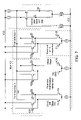
It is known in the prior art to have dual mode comparators. Dual mode comparators are often used in automatic testing equipment (ATE) for testing one or more devices under tests (DUTs). Dual mode comparators can operates in any one of a plurality of modes including a differential mode, a common mode, and single-ended mode wherein the mode is selectable based upon an external selection signal provided to the dual mode comparator. The prior art designs provide separate circuitry for each of the modes. Additionally, for each comparison, there is a separate normal windowing comparator (NWC) as shown in FIG. 1.
FIG. 1 shows two inputs provided into the prior art dual mode comparator circuit, which are labeled DUT1 101 and DUT2 102. These inputs are each coupled to a device under test. These inputs may be attached to two separate inputs from a single device or the inputs may be coupled to two separate devices. The circuit includes a pair of output multiplexors (MUX) 103, 104. Each multiplexor receives a control signal that determines the selected comparator mode to output. Thus, by way of example, for the first multiplexor 103, each NWC 110, 111, 112, 113 is active and produces an output signal. Therefore, the multiplexor 103 receives in four input signal and selects two of the four input signals to output (either a single ended comparison of DUT1 with VOH1 and a single ended comparison of DUT1 with VOL1, or a differential comparison with VOH1 and a differential comparison with VOL1). As a result, each NWC 110, 111, 112, 113 circuit is always active. Each NWC 110, 111, 112, 113 circuit includes at least two stages, a comparison stage and an amplification stage. Therefore, the prior art configuration always requires power for the NWC.
SUMMARY OF THE INVENTION
A dual mode comparator circuit is disclosed. The dual mode comparator includes a plurality of differential transistor pairs. Each differential transistor pair includes a plurality of inputs and outputs. The outputs of the differential transistor pairs are coupled to inputs of a multiplexor. The multiplexor includes at least one control input for selecting between the multiplexor inputs and provides the selected input to the multiplexor output. The dual mode comparator further includes a comparator back end that is coupled to the output of the multiplexor. The comparator back end may include a folded cascode and additional gain stages. The comparator back end provides the comparator output to the next stage. The dual mode comparator may be used in automatic testing equipment embodiments wherein both power and space are at a premium. The disclosed dual mode comparator circuit reduces both the required power and reduces the silicon area need to implement the dual mode comparator as compared with the prior art.
In certain embodiments, the differential transistor pairs are formed from a plurality of bipolar transistors. In other embodiments, other transistor types, such as, CMOS transistors may be employed. In embodiments that use the bipolar transistors, the bipolar transistors each include an emitter, collector and base. The input for each differential transistor pair is received into the base of the transistors. The multiplexor is coupled to the collector of the bipolar transistors. A current source is provided at the emitters of the differential bipolar transistor pairs. In one embodiment, additional current sources are coupled between the output of the multiplexor and the input of the comparator back end. In other embodiments, additional current sources may be coupled between the differential transistor pairs and the inputs to the multiplexor.
During operation, the multiplexor will route the differential input signal from the differential transistor pair either to the comparator back end or to a voltage rail. Thus, there are two states for each input to the multiplexor. The multiplexor can be formed from a plurality of bipolar transistor pairs where the emitters of an input pair of transistors of the multiplexor are coupled to the collectors of a differential transistor pair and the collectors of an output pair of transistors of the multiplexor are coupled to a comparator back end.
Also disclosed is a method for selection of an input signal in a dual mode comparator. First, an input signal is compared with another signal (either a reference voltage or another input signal) using a differential transistor pair. The differential transistor pair generates an output based upon the two input signals. A multiplexor is coupled to the output of the differential transistor pair, where a selection signal is received by the multiplexor and the output of the desired differential transistor pair is received by the comparator back end. The comparator back end includes a gain stage that amplifies the desired differential signal.
Embodiments of the dual mode comparator reduce the number of gain stages, since a single comparator back end may be shared by a plurality of comparator front ends/differential transistor pairs.
The dual mode comparator benefits from operating in the current domain, such that the additional capacitance that occurs due to the additional circuitry being coupled to the input node of the front end does not decrease performance.
BRIEF DESCRIPTION OF THE DRAWINGS
The foregoing features of the invention will be more readily understood by reference to the following detailed description, taken with reference to the accompanying drawings, in which:
FIG. 1 is a diagram of a prior art dual mode comparator;
FIG. 2 is a diagram of one embodiment of the dual mode comparator circuit invention;
FIG. 3 is a flow chart that describes a method of processing a signal in a dual mode comparator;
FIG. 4 is a circuit schematic showing a first embodiment of the invention;
FIG. 5 is a circuit schematic showing an alternative embodiment of the invention;
FIG. 6 is a circuit schematic showing an alternative embodiment of the invention wherein multiple differential transistor pairs are coupled to the multiplexor; and
FIG. 7 is a circuit schematic showing an embodiment of the invention where two differential signals are passed to the comparator back end simultaneously through the multiplexor.
DETAILED DESCRIPTION OF SPECIFIC EMBODIMENTS
As used in the following detailed description and appended claims, the term “dual-mode” shall refer to a comparator's ability to selectably operate in more than one mode for comparing signals (e.g. single-ended mode, differential mode, common mode). The term “comparator back end” shall refer to passive or active circuitry that completes the first gain stage of a comparator subsequent to a differential transistor pair and the comparator back end may contain additional gain stages.
FIG. 2 is a dual mode comparator circuit 200 that performs all of the functions of FIG. 1, but reduces the redundancy of the window comparators. In FIG. 2, the front-end of each comparator is separated from the back-end. Thus, the differential transistor pair that is used for performing the comparison is coupled to a multiplexor and the comparator back end is shared by more than one differential transistor pair. In this configuration, as compared to FIG. 1, the number of comparator back ends that are required is reduced by half. Thus, the number of gain stages is reduced, thereby significantly reducing the power consumption and silicon area. The dual mode comparator of FIG. 2 may be used in ATE applications where both reduction of silicon area and power consumption are desirable. The dual mode comparator may be part of the pin electronics for a channel of the ATE. A channel is defined by an association of pin electronics with one or more pins of a device under test (DUT). Pin electronics include, but are not limited to, comparators, load circuitry, driver circuitry and parametric measurement units. The dual mode comparator may be formed on a silicon wafer along with other ATE specific pin electronic circuitry. Current automatic testing equipment can test hundreds to thousands of pins of DUTs simultaneously. Thus, by reducing the silicon area and power consumption for the pin electronics additional pin electronics can be added to the ATE and more DUT pins tested.
The dual mode comparator 200 includes a pair of inputs 201, 202. The two inputs are coupled to devices under test (DUTs) that produce input signals. The first stage for each input signal is a single ended buffer 203, 204 that buffers the signals within the dual mode comparator from the connected DUT. The output of the single-ended buffer for DUT1 is coupled to the input of two front end differential mode/single ended multiplexors (DM/SE Mux) 205, 206. The first front end DM/SE Mux 205 includes both a differential mode and a single ended mode of operation. Depending on the control signal provided to the front end DM/SE MUX 205, the front end DM/SE MUX 205 will either compare the differential input signal (input signal of DUT1−input signal of DUT2) with a known comparison signal, VOH1 or compare the input signal of DUT1 to VOH1. The front end DM/SE MUX 205 outputs the comparison signal to the comparator back-end 207 that includes a gain stage. Thus, two comparisons are performed wherein only a single comparator back end 207 is used. The second front end DM/SE MUX 206 operates substantially the same as the first; however, comparisons are made with VOL1 instead of VOH1.
Looking at the lower half of the circuit, a common mode buffer 210 receives both the input signals from the DUT1 and DUT2. The common mode buffer creates a common mode signal from the two input signals by adding the signals together and dividing the resulting signal in half. A front end common mode/single ended multiplexor (CM/SE MUX) 211 receives as input the output of the CM buffer 210 and additionally receives in the input signal from DUT2. Thus, depending on the control signal received by the multiplexor, the front end CM/SE MUX 211 will compare either the common mode signal with a known level, VOH2 or compare the input signal from DUT2 with VOH2. A comparator back end 212 then receives the selected signal from the front end CM/SE MUX 211 and amplifies the differential signal to a desired level producing QHI2. The fourth front end, front end CM/SE MUX 213 operates the same as the third front end except the comparisons are made with VOL2 and the output from the dual mode comparator is QLO2.
FIG. 3 is a flow chart that describes the methodology of processing a signal in one embodiment of the invention. The dual mode comparator receives in as input a voltage signal. The voltage signal can be generated by a DUT. The signal is fed into the input of a differential transistor pair. At the other input of the differential transistor pair is a comparison signal. In some embodiments, the comparison signal is at a known level (Ref). In other embodiments, the comparison signal may be a voltage signal from another input. The differential transistor pair produces a differential current output 300. A control signal is received by a multiplexor positioned between the differential transistor pair and a comparator back end. The control signal causes the multiplexor to select from a plurality of differential transistor pairs and provides the differential current to the comparator back end 310. The comparator back end amplifies the differential current output produced by the selected differential transistor pair 320.
FIG. 4 is a circuit schematic showing a first embodiment of the dual mode comparator. As shown, there are two sets of differential transistor pairs 401, 402 capable of receiving input signals D1, D2 and comparing the signals to a reference (Ref) in the dual mode comparator circuit 400. Although two sets of differential transistor pairs are shown, the invention should not be seen as limited to two inputs. Additionally, although the figure shows the differential transistor pairs as bipolar transistors, other transistors may be substituted without deviating from the scope of the invention. Input signal D1 is applied as input to the first differential transistor pair 401 and input signal D2 is applied to the second differential transistor pair 402. The signals D1 and D2 are compared to a second signal marked Ref, which can be a reference signal (Vol, Vhi, Vt etc.) or another input signal. The second signal for each of the differential transistor pairs may be the same signal (i.e. D1 and D2 are compared to the same reference) or the signal may be different (i.e. D1 is compared to a first reference signal and D2 is compared to a second reference signal). The output of the differential transistor pairs are each coupled to inputs of the multiplexor 403. In this embodiment, the multiplexor inputs are the collectors of the bipolar transistors 404, 405. The multiplexor includes a plurality of bipolar transistors Q5-Q12. In this embodiment of the multiplexor, differential transistor pairs are controlled by an input signal that is either S1 or the inverse of S1, S1B. If S1 is high Q5 and Q7 are active and the output of the second transistor pair 402 is coupled to the rail Vcc. Additionally, if S1 is high Q10 and Q12 are active and the output of the first transistor pair 401 is coupled to the comparator back end 406 which is a folded cascode including transistors Q13, 14. If the inverse S1B is high, transistors Q6, Q8, Q9 and Q11 are active and the output 404 of the first transistor pair 401 is coupled to the voltage rail Vcc while the output 405 of the second transistor pair 402 is coupled to the comparator back end 406. As a result, only a single comparator back end is necessary for the operation of either of the two comparisons. In the configuration of FIG. 4, there is only a single control signal that is used to control the switching between the differential transistor pairs. In other embodiments in which there are more differential transistor pairs coupled to the multiplexor, additional control signals could be used for selecting the appropriate output.
FIG. 5 is an alternative embodiment of FIG. 4. In this embodiment, the current sources 510, 520, 530, 540 that provide current to the comparator back end 504 are coupled to the inputs 511, 512, 531, 532 of the multiplexor 503 as opposed to the output of the multiplexor as shown in FIG. 4. In this embodiment, four current sources 510, 520, 530, 540 are necessary to provide current to each of the possible inputs 511,512,531,532 to the multiplexor 503. In contrast, in FIG. 4, only two current sources 410, 420 are necessary, since current is only need for the selected signal that is output from the multiplexor 403. FIG. 5 operates substantially the same as the embodiment of FIG. 4. Input signals D1, D2 are applied to the differential transistor pairs which cause a differential current draw from the current sources 510, 520, 530, 540. In this embodiment, the multiplexor circuitry 503 operates both as a multiplexor and acts as a folded cascode. In FIG. 4, transistors Q13 and Q14 of the comparator back end function as a folded cascode. Depending upon whether signal S1 or S1B is high, the multiplexor 503 will direct the current from the current sources 510,520 or 530, 540 minus the current drawn away as a result of the differential transistor pairs 501 or 502 to the output of the multiplexor. The output of the multiplexor is coupled to another cascode circuit 550. This cascode 550 is included to provide a lower capacitance at the output node. The cascode 550 is not necessary for operation of the dual mode comparator 500. The output of the cascode is provided to the comparator back end 504 and the differential current/voltage can be sampled at Q and QB.
FIG. 6 is another embodiment of the dual mode comparator. In this embodiment, three differential transistor pairs (601, 602, and 603) are shown. The differential transistor pairs are coupled to the multiplexor 610. The multiplexor is subdivided into three sections 604, 605, 606, wherein each section is associated with one of the differential transistor pairs 601, 602, 603. For each section of the multiplexor, a different control signal S1, S2, S3 is used. Under normal operation, If S1 is high, the differential signal from the 1st differential transistor pair 601 is passed to the comparator back end 607, and both S2B and S3B are active causing the signals from the 2nd and 3rd differential transistor pairs 602, 603 to be coupled to the voltage rail VCC. Similarly, if S2 is active S1B and S3B would be active coupling the 1st and 3rd differential transistor pairs 601, 603 to the voltage rail VCC and passing the differential signal from the 2nd differential transistor pair 602 to the comparator back end 607. Likewise, if S3 is active S1B and S2B are active and only the differential signal from the 3rd differential transistor pair is passed to the comparator back end.
In certain embodiments, where an offset signal is desired for an output signal such as that shown in FIG. 7, the multiplexor 700 may pass to the comparator back end 710 more than one differential signal from more than one differential transistor pair simultaneously. For example, if the differential transistor pair delineated Diff Stage 720 receives in as input a differential signal (Dut1 signal−Dut2 signal), and an offset input voltage is desired for the differential signal 720, the output signal from the differential transistor pair delineated Offset Stage 730 may be passed through the multiplexor 700 simultaneously with the output signal of the Diff Stage transistor pair 720 to the comparator back end 710. In such an embodiment, both the Offset Stage 720 and Diff Stage 730 are coupled to a front end Mux 2 740 that is part of the Mux 700. The Front End Mux 2 740 is controlled by a single control signal S2. Thus, when S2 is active (high) both the Diff Stage 720 and the Offset Stage 730 pass their signals to the comparator back end 710.
As shown in FIGS. 4-7 the comparator back end completes the gain stage formed in combination with the selected differential transistor pair, however additional gain stages may be coupled to the comparator back end without deviating from the inventive concept. It should also be noted that FIGS. 4-7 show simple differential transistor pairs and do not show the coupled single ended buffer, the differential mode buffer or the common mode buffer shown in FIG. 2. These buffers may be implemented in a plurality of ways as are known to those of ordinary skill in the art.
Although various exemplary embodiments of the invention have been disclosed, it should be apparent to those skilled in the art that various changes and modifications can be made which will achieve some of the advantages of the invention without departing from the true scope of the invention. These and other modifications are intended to be covered by the appended claims.

Claims (19)

1. A dual mode comparator circuit comprising:
a first differential transistor pair having two inputs and outputs;
a second differential transistor pair having two inputs and outputs;
a third differential transistor pair having two inputs and outputs;
a multiplexor having at least one control input for selecting the outputs of the first differential transistor pair, the outputs of the second differential transistor pair, and the outputs of the third differential transistor pair, wherein the outputs of the second differential transistor pair and the outputs of the third differential transistor pair are selectively passed simultaneously.
2. A dual mode comparator circuit according to claim 1 further comprising:
a comparator back end coupled to the output of the multiplexor.
3. A dual mode comparator circuit according to claim 2, wherein the comparator back end includes a cascode stage.
4. A dual mode comparator circuit according to claim 1, wherein the first differential transistor pair, the second differential transistor pair, and the third differential pair comprise bipolar transistors, each having a collector, emitter and base.
5. A dual mode comparator circuit according to claim 4, wherein the multiplexor is electrically coupled to each collector of the bipolar transistors of the first, second, and third differential transistor pairs.
6. A dual mode comparator circuit according to claim 5, wherein in a first state the multiplexor couples the collectors of the second and the third differential transistor pairs with a voltage rail and in a second state the multiplexor couples the collectors of the second and third differential transistor pairs with a current source.
7. A dual mode comparator circuit according to claim 5, wherein the emitters of an input pair of transistors of the multiplexor are coupled to the collectors of the first differential transistor pair and the collectors of an output pair of transistors of the multiplexor are coupled to a comparator back end.
8. A dual mode comparator circuit according to claim 1, wherein the third differential transistor pair provides an offset voltage for the output of the second differential pair.
9. A method for selecting a signal in a dual mode comparator, the method comprising:
receiving a first single-ended signal;
receiving a second single-ended signal;
receiving a reference signal;
in response to a selection signal, selecting with a multiplexor either a differential output signal resulting from a comparison of the first and second single-ended signals or a single-ended output signal resulting from a comparison of the first single-ended signal with the reference signal; and
providing the selected output signal to a gain stage circuit.
10. The method according to claim 9, wherein the first and second single-ended signals originate from a plurality of ports of one or more devices under test.
11. The method according to claim 9, wherein the comparison is performed using a differential transistor pair.
12. The method according to claim 11, wherein the dual mode comparator includes a plurality of differential transistor pairs each coupled to selectable inputs of the multiplexor.
13. The method according to claim 11, wherein the first single-ended and second single-ended signals are voltages and the selected output signal is proportional to a resulting differential voltage of the differential transistor pair.
14. A method according to claim 11, wherein the differential transistor pair is a bipolar differential transistor pair.
15. The method according to claim 9, wherein the gain stage circuit includes a cascode amplifier.
16. The method according to claim 9, wherein the dual mode comparator operates within automatic testing equipment and tests signals from one or more device under test.
17. A dual mode comparator circuit, the dual mode comparator circuit comprising:
at least three differential transistor pairs each having a plurality of inputs and at least one output;
a multiplexor coupled to the output of each of the at least three differential transistor pairs, the multiplexor including an input for receiving a selection signal; and
a comparator back end;
wherein the multiplexor selectively couples the output of a plurality of differential transistor pairs simultaneously with the comparator back end.
18. A dual mode comparator circuit according to claim 17, wherein the comparator back end includes a cascade stage.
19. A dual mode comparator circuit according to claim 17, wherein the comparator back end produces an output, and wherein the output is a differential signal proportional to a differential input signal received at the inputs of the selected one or more differential transistor pairs.
US11/409,712 2005-04-25 2006-04-24 Dual mode comparator Active 2026-05-18 US7474129B2 (en)

Priority Applications (1)

Application Number Priority Date Filing Date Title
US11/409,712 US7474129B2 (en) 2005-04-25 2006-04-24 Dual mode comparator

Applications Claiming Priority (2)

Application Number Priority Date Filing Date Title
US67458005P 2005-04-25 2005-04-25
US11/409,712 US7474129B2 (en) 2005-04-25 2006-04-24 Dual mode comparator

Publications (2)

Publication Number Publication Date
US20060250165A1 US20060250165A1 (en) 2006-11-09
US7474129B2 true US7474129B2 (en) 2009-01-06

Family

ID=37393492

Family Applications (1)

Application Number Title Priority Date Filing Date
US11/409,712 Active 2026-05-18 US7474129B2 (en) 2005-04-25 2006-04-24 Dual mode comparator

Country Status (1)

Country Link
US (1) US7474129B2 (en)

Cited By (1)

* Cited by examiner, † Cited by third party
Publication number Priority date Publication date Assignee Title
US8513980B2 (en) 2011-10-25 2013-08-20 Texas Instruments Incorporated Reduced offset comparator

Families Citing this family (2)

* Cited by examiner, † Cited by third party
Publication number Priority date Publication date Assignee Title
US7705655B2 (en) * 2006-09-18 2010-04-27 Micrel, Inc. Input buffer circuit
US10659022B2 (en) * 2016-01-07 2020-05-19 Sony Corporation Comparator, analog-to-digital converter, solid-state image pickup device, and image pickup apparatus

Citations (4)

* Cited by examiner, † Cited by third party
Publication number Priority date Publication date Assignee Title
US5191234A (en) * 1990-12-10 1993-03-02 Sony Corporation Pulse signal generator and cascode differential amplifier
US5430400A (en) * 1993-08-03 1995-07-04 Schlumberger Technologies Inc. Driver circuits for IC tester
US5465072A (en) * 1994-08-05 1995-11-07 Linear Technology Corporation Tunable operational transcondunctance amplifier having high linearity
US20050184791A1 (en) * 2004-02-24 2005-08-25 Bernd Neumann Method and system for multichannel-isolation-technique multiplexer

Patent Citations (4)

* Cited by examiner, † Cited by third party
Publication number Priority date Publication date Assignee Title
US5191234A (en) * 1990-12-10 1993-03-02 Sony Corporation Pulse signal generator and cascode differential amplifier
US5430400A (en) * 1993-08-03 1995-07-04 Schlumberger Technologies Inc. Driver circuits for IC tester
US5465072A (en) * 1994-08-05 1995-11-07 Linear Technology Corporation Tunable operational transcondunctance amplifier having high linearity
US20050184791A1 (en) * 2004-02-24 2005-08-25 Bernd Neumann Method and system for multichannel-isolation-technique multiplexer

Cited By (1)

* Cited by examiner, † Cited by third party
Publication number Priority date Publication date Assignee Title
US8513980B2 (en) 2011-10-25 2013-08-20 Texas Instruments Incorporated Reduced offset comparator

Also Published As

Publication number Publication date
US20060250165A1 (en) 2006-11-09

Similar Documents

Publication Publication Date Title
US7154259B2 (en) Isolation buffers with controlled equal time delays
US7498847B2 (en) Output driver that operates both in a differential mode and in a single mode
US9813050B1 (en) Comparator circuit with input attenuator
JPH06112795A (en) Signal changeover circuit and signal generation circuit
US6448806B1 (en) Circuit for providing a logical output signal in accordance with crossing points of differential signals
US7474129B2 (en) Dual mode comparator
US7345542B2 (en) Circuit and method for avoiding circuit performance degradation caused by time-variable thermal imbalances
US6262585B1 (en) Apparatus for I/O leakage self-test in an integrated circuit
US8207725B2 (en) Tester having device under test power supply
KR19990073014A (en) Chopper type voltage comparing circuit capable of correctly determining output polarity, and voltage comparing method
US20020030535A1 (en) Dynamic bias circuitry utilizing early voltage clamp and translinear techniques
US7583146B2 (en) Balanced differential cross-coupled transconductance amplifier for a multiplexor
US7091741B2 (en) Input buffer capable of reducing input capacitance seen by input signal
Simpson et al. An integrated, CMOS, constant-fraction timing discriminator for multichannel detector systems
CN111313871B (en) Dynamic pre-amplification circuit and dynamic comparator
JP7307110B2 (en) Comparator with configurable mode of operation
US7755377B2 (en) Driver circuit and test apparatus
US9077301B2 (en) Nanovolt amplifier design
KR100346632B1 (en) Delay device, semiconductor testing device, semiconductor device, and oscilloscope
US7952359B2 (en) Test apparatus having bidirectional differential interface
US20210199700A1 (en) Dc power rail probes and measurement methods
US7088146B1 (en) Apparatus and method for high-speed half-latch with low overdrive voltage
US6518797B2 (en) Current mode logic circuit with output common mode voltage and impedance control
US9172362B2 (en) Multifunction word recognizer element
US6822435B2 (en) Comparator circuit for differential swing comparison and common-mode voltage comparison

Legal Events

Date Code Title Description
AS Assignment

Owner name: ANAALOG DEVICES, INC., MASSACHUSETTS

Free format text: ASSIGNMENT OF ASSIGNORS INTEREST;ASSIGNOR:CAREY, BRIAN;REEL/FRAME:017789/0076

Effective date: 20060523

AS Assignment

Owner name: ANALOG DEVICES, INC., MASSACHUSETTS

Free format text: CORRECTIVE ASSIGNMENT TO CORRECT THE SPELLING OF THE ASSIGNEE'S NAME FROM ANAALOG DEVICES, INC. TO ANALOG DEVICES, INC. PREVIOUSLY RECORDED ON REEL 017789 FRAME 0076;ASSIGNOR:CAREY, BRIAN;REEL/FRAME:018128/0589

Effective date: 20060523

STCF Information on status: patent grant

Free format text: PATENTED CASE

FPAY Fee payment

Year of fee payment: 4

FPAY Fee payment

Year of fee payment: 8

MAFP Maintenance fee payment

Free format text: PAYMENT OF MAINTENANCE FEE, 12TH YEAR, LARGE ENTITY (ORIGINAL EVENT CODE: M1553); ENTITY STATUS OF PATENT OWNER: LARGE ENTITY

Year of fee payment: 12