US7471147B2 - Automatic gain controller - Google Patents
Automatic gain controller Download PDFInfo
- Publication number
- US7471147B2 US7471147B2 US11/403,905 US40390506A US7471147B2 US 7471147 B2 US7471147 B2 US 7471147B2 US 40390506 A US40390506 A US 40390506A US 7471147 B2 US7471147 B2 US 7471147B2
- Authority
- US
- United States
- Prior art keywords
- signal
- differential signal
- wave
- level
- reference voltage
- Prior art date
- Legal status (The legal status is an assumption and is not a legal conclusion. Google has not performed a legal analysis and makes no representation as to the accuracy of the status listed.)
- Expired - Fee Related, expires
Links
Images


Classifications
-
- G—PHYSICS
- G11—INFORMATION STORAGE
- G11B—INFORMATION STORAGE BASED ON RELATIVE MOVEMENT BETWEEN RECORD CARRIER AND TRANSDUCER
- G11B20/00—Signal processing not specific to the method of recording or reproducing; Circuits therefor
- G11B20/10—Digital recording or reproducing
-
- H—ELECTRICITY
- H03—ELECTRONIC CIRCUITRY
- H03G—CONTROL OF AMPLIFICATION
- H03G3/00—Gain control in amplifiers or frequency changers without distortion of the input signal
- H03G3/20—Automatic control
- H03G3/30—Automatic control in amplifiers having semiconductor devices
- H03G3/3036—Automatic control in amplifiers having semiconductor devices in high-frequency amplifiers or in frequency-changers
-
- G—PHYSICS
- G11—INFORMATION STORAGE
- G11B—INFORMATION STORAGE BASED ON RELATIVE MOVEMENT BETWEEN RECORD CARRIER AND TRANSDUCER
- G11B20/00—Signal processing not specific to the method of recording or reproducing; Circuits therefor
- G11B20/10—Digital recording or reproducing
- G11B20/10009—Improvement or modification of read or write signals
- G11B20/10018—Improvement or modification of read or write signals analog processing for digital recording or reproduction
- G11B20/10027—Improvement or modification of read or write signals analog processing for digital recording or reproduction adjusting the signal strength during recording or reproduction, e.g. variable gain amplifiers
-
- G—PHYSICS
- G11—INFORMATION STORAGE
- G11B—INFORMATION STORAGE BASED ON RELATIVE MOVEMENT BETWEEN RECORD CARRIER AND TRANSDUCER
- G11B7/00—Recording or reproducing by optical means, e.g. recording using a thermal beam of optical radiation by modifying optical properties or the physical structure, reproducing using an optical beam at lower power by sensing optical properties; Record carriers therefor
- G11B7/08—Disposition or mounting of heads or light sources relatively to record carriers
- G11B7/09—Disposition or mounting of heads or light sources relatively to record carriers with provision for moving the light beam or focus plane for the purpose of maintaining alignment of the light beam relative to the record carrier during transducing operation, e.g. to compensate for surface irregularities of the latter or for track following
-
- H—ELECTRICITY
- H03—ELECTRONIC CIRCUITRY
- H03G—CONTROL OF AMPLIFICATION
- H03G3/00—Gain control in amplifiers or frequency changers without distortion of the input signal
- H03G3/20—Automatic control
- H03G3/30—Automatic control in amplifiers having semiconductor devices
- H03G3/3084—Automatic control in amplifiers having semiconductor devices in receivers or transmitters for electromagnetic waves other than radiowaves, e.g. lightwaves
Definitions
- the invention relates to an automatic gain controller. More particularly, the present invention relates to an automatic gain controller that receives an input signal and can output an output signal with the amplitude maintained constant, without using an operational amplifier for shifting the direct current (DC) level of the output signal.
- DC direct current
- An optical disk may be classified into a write-once disk such as a CD-ROM and a DVD-ROM, and a rewritable disk such as a CD-RW, a DVD-RW, and a DVD-RAM.
- the rewritable disk cannot generate a clock signal from a reproduced signal, unlike an existing read-only disk. Accordingly, grooves of the disk on which information is recorded are wobbled for a predetermined period, and a clock signal required for a recording operation is generated by detecting this wobble signal.
- FIG. 1 is a block diagram of a conventional wobble signal reproducing apparatus
- FIGS. 2 A-C are views illustrating a wobble signal reproducing process performed by the apparatus of FIG. 1 .
- wobble signals are measured at regions A, B, C and D on a disk 10 .
- Quantities of light corresponding to the wobble signals measured at the regions A and D are added together by an adder 20 a
- quantities of light corresponding to the wobble signals measured at the regions B and C are added together by an adder 20 b .
- a signal A+D outputted from the adder 20 a and a signal B+C outputted from the adder 20 b have RF signals having the same phase and wobbling signals having a phase difference of 180° with each other as shown in FIGS. 2A and 2B .
- the signal A+D and the signal B+C are filtered by high-pass filters (HPF) 30 a and 30 b having a cutoff frequency enough to pass the wobble signals, respectively, and thus DC offsets thereof are eliminated.
- HPF high-pass filters
- a subtracter 50 subtracts the signal B+C from the signal A+D, which are gain-adjusted by the automatic gain controllers 40 a and 40 b , to output the wobble signal as shown in FIG. 2C .
- a band-pass filter (BPF) 60 having a narrow band detects a wobble signal having a high signal-to-noise ratio (S/N) from the output wobble signal, and after the automatic gain controller (AGC) 70 amplifies the gain of the wobble signal, a comparator 80 quantizes the wobble signal and outputs a wobble clock signal.
- BPF band-pass filter
- AGC automatic gain controller
- FIG. 3 is a view illustrating the construction of a conventional automatic gain controller
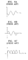
- FIGS. 4A through 4B are views illustrating waveforms of the signal from each terminal of the automatic gain controller shown in FIG. 3 .
- an automatic gain controller 40 a includes a variable gain amplifier (VGA) 41 , a high-pass filter (HPF) 42 , a signal level detection unit 43 , and a comparison unit 44 .
- VGA variable gain amplifier
- HPF high-pass filter
- the variable gain amplifier 41 amplifies an input signal Vin with a predetermined amplification gain a according to a control voltage V control input from the comparison unit 44 , and outputs a first differential signal Vp′, a second differential signal Vn′ having a 180° phase difference from the first differential signal Vp′, and an output signal Vout obtained by subtracting the second differential signal Vn′ from the first differential signal Vp′.
- the gain ⁇ is increased in proportion to the control voltage V control
- the input signal Vin has a voltage Vref as a DC level.
- the high-pass filter (HPF) 42 shifts DC levels of the first differential signal Vp′ and the second differential signal Vn′ to the DC level Vref of the input signal Vin to output the DC-level-shifted differential signals.
- the signal level detection unit 43 full-wave-rectifies first and second differential signals Vp and Vn, and extracts a DC component from the full-wave-rectified signal Vfr to output the extracted DC component. More specifically, the signal level detection unit 43 includes a full-wave rectifier 43 - 1 and a low-pass filter 43 - 2 .
- the full-wave rectifier 43 - 1 full-wave-rectifies the first differential signal Vp and the second differential signal Vn which are output from the high-pass filter 42 .
- the low-pass filter 43 - 2 extracts the DC component from the signal Vfr full-wave-rectified by the full-wave rectifier 43 - 1 .
- the reference voltage Vref added to the effective value ⁇ A/ ⁇ square root over (2) ⁇ of the AC component of the output signal Vout makes Vref+( ⁇ A/ ⁇ square root over ( 2 ) ⁇ ), which is equal to the magnitude of the DC component of the full-wave-rectified signal Vfr.
- the comparison unit 44 receives the output voltage V_lpf of the low-pass filter 43 - 2 and a reference voltage V_level and compares them with each other. If the output voltage V_lpf of the low-pass filter 43 - 2 is lower than the reference voltage V_level, the comparison unit 44 increases the gain of the variable gain amplifier 41 by heightening the control voltage Vcontrol. Thus, the peak-peak voltage of the output signal Vout is increased.
- the comparison unit 44 decreases the gain of the variable gain amplifier 41 by lowering the control voltage Vcontrol.
- the peak-to-peak voltage of the output signal Vout is decreased. If the output voltage V_lpf of the low-pass filter 43 - 2 reaches the reference voltage V_level, the output signal Vout is output with a constant magnitude of the peak-peak voltage.
- the comparison unit 44 controls the reference voltage V-level to have a magnitude of Vref+(Vpp/ 2 ⁇ square root over (2) ⁇ ).
- Vpp/ 2 ⁇ square root over (2) ⁇ is an effective value of a target peak-peak voltage Vpp of the output signal Vout.
- FIG. 5 is a view illustrating the detailed construction of a signal level detection unit in FIG. 3 .
- FIGS. 6A through 6E are views illustrating signal waveforms appearing at respective points of the signal level detection unit in FIG. 3 .
- the signal level detection unit 43 includes the full-wave rectifier 43 - 1 composed of first through third transistors Q n1 , Q n2 , and Q n3 and an operational amplifier OP-Amp, and the low-pass filter 43 - 2 composed of a resistor R and a capacitor C.
- the pair of the first and second transistors Q n1 and Q n2 full-wave-rectify the first and second differential signals Vp ( FIG. 6B ) and Vn ( FIG. 6A ).
- the DC level Vref′ of the signal V A ( FIG. 6C ) outputted from the first and second transistors Q n1 and Q n2 is lowered as much as the DC voltage V GS between the gates and sources of the first and second transistors Q n1 and Q n2 from the reference voltage Vref.
- Vref′ Vref ⁇ V GS .
- the operational amplifier OP-Amp and the third transistor Q n3 increase the DC level of the full-wave-rectified signal V A as mush as V GS .
- the conventional automatic gain controller employs the operational amplifier OP-Amp in order to shift the DC level of the full-wave-rectified signal VA to Vref.
- random offset voltages exist in the operational amplifier due to the mismatching of a manufacturing process.
- the offset voltage is generally in the range of several tens of mV.
- Exemplary embodiments of the present invention overcome the above disadvantages and other disadvantages not described above. Also, the present invention is not required to overcome the disadvantages described above, and an exemplary embodiment of the present invention may not overcome any of the problems described above.
- An aspect of the present invention is to provide an automatic gain controller that receives an input signal and can output an output signal with the amplitude maintained constant, without using an operational amplifier for shifting the DC level of the output signal.
- An aspect of the present invention provides an automatic gain controller which comprises a variable gain amplifier for amplifying an input signal having a specified DC level on the basis of the DC level, and outputting a first differential signal having a specified gain ⁇ , a second differential signal having a 180° phase difference from the first differential signal, and an output signal obtained by subtracting the second differential signal from the first differential signal; a full-wave-rectifying unit for receiving and full-wave-rectifying the first differential signal and the second differential signal; a low-pass filter for extracting the DC component from the output signal of the full-wave-rectifying unit and outputting the extracted DC component; a reference voltage level adjustment unit for receiving a desired reference voltage and adjusting a DC level of the reference voltage as much as a variation of the DC level produced when the first differential signal and the second differential signal are full-wave-rectified; and a comparison unit for comparing the output signal of the low-pass filter with the output signal of the reference voltage level adjustment unit to adjust a gain of the variable gain amplifier.
- the comparison unit may decrease the gain of the variable gain amplifier, and if the output signal of the low-pass filter is lower than the output signal of the reference voltage level adjustment unit, the comparison unit may increase the gain of the variable gain amplifier.
- the reference voltage may have a magnitude obtained by adding an effective value of a target peak-to-peak voltage of the output signal to the DC level.
- the full-wave-rectifying unit may include a first transistor for half-wave-rectifying the first differential signal received through its gate, and outputting the half-wave-rectified first differential signal to its source; and a second transistor for half-wave-rectifying the second differential signal received through its gate, and outputting the half-wave-rectified second differential signal to its source, wherein a connection point of the source of the first transistor and the source of the second transistor is connected to an input terminal of the low-pass filter.
- the reference voltage level adjustment unit may include a third transistor for lowering the DC level of the reference voltage received through its gate as much as the variation of the DC level, and outputting the reference voltage with its DC level lowered to its source.
- the first through third transistors may be N-type metal-oxide-semiconductor (NMOS) transistors.
- NMOS N-type metal-oxide-semiconductor
- the first through third transistors may have the same characteristic, and be driven by a bias current having the same magnitude.
- the automatic gain controller may further comprise a high-pass filter for level-shifting the first and second differential signals output from the variable gain amplifier so that the first and second differential signals have the same DC level, and outputting the DC-level-shifted first and second differential signals to the full-wave-rectifying unit.
- FIG. 1 is a block diagram of a conventional wobble signal reproducing apparatus
- FIGS. 2A through 2C are views illustrating a wobble signal reproducing process performed by the apparatus as shown in FIG. 1 .
- FIG. 3 is a diagram illustrating the construction of a conventional automatic gain controller
- FIGS. 4A through 4F are views illustrating waveforms of signals appearing at respective points of the automatic gain controller as shown in FIG. 3 ;
- FIG. 5 is a view illustrating the detailed construction of the signal level detection unit of FIG. 3 ;
- FIGS. 6A through 6E are views illustrating signal waveforms appearing at respective points of the signal level detection unit of FIG. 3 ;
- FIG. 7 is a circuit diagram of an automatic gain controller according to an exemplary embodiment of the present invention.
- FIGS. 8A through 8G are views illustrating signal waveforms appearing at respective points of the automatic gain controller of FIG. 7 ;
- FIGS. 9A through 9D are views provided for comparison of variation among chips in which the conventional first and second automatic gain controllers are connected in parallel, with variation among chips in which first and second automatic gain controllers according to the present invention are connected in parallel;
- FIGS. 10A and 10B are views provided for comparison of the mismatching of the output signals of the conventional first and second automatic gain controllers connected in parallel, with the mismatching of the output signals of first and second automatic gain controllers according to the present invention connected in parallel.
- FIG. 7 is a circuit diagram of an automatic gain controller according to an exemplary embodiment of the present invention.
- FIGS. 8A through 8 G are views illustrating signal waveforms appearing at respective points of the automatic gain controller, as shown in FIG. 7 .
- an automatic gain controller 100 includes a variable gain amplifier (VGA) 110 , a high-pass filter (HPF) 120 , a level detection unit 130 , and a comparison unit 140 .
- VGA variable gain amplifier
- HPF high-pass filter
- the variable gain amplifier 110 amplifies an input signal Vin having Vref 1 as a DC level according to a magnitude of a control voltage Vcontrol, and outputs a first differential signal Vp′ having a desired gain ⁇ , a second differential signal Vn′ having a 180° phase difference from the first differential signal Vp′, and an output signal Vout obtained by subtracting the second differential signal Vn′ from the first differential signal Vp′.
- the gain ⁇ is increased in proportion to the magnitude of the control voltage Vcontrol.
- the high-pass filter (HPF) 120 level-shifts a reference voltage of the first differential signal Vp′ and the second differential signal Vn′ to the DC level Vref 1 of the input signal Vin.
- the level detection unit 130 full-wave-rectifies a first differential signal Vp and a second differential signal Vn, and extracts a DC component from the full-wave-rectified signal Vc.
- the level detection unit 130 includes a full-wave rectifier 131 and a low-pass filter 132 .
- the full-wave rectifier 131 includes a pair of first and second NMOS transistors (N-type metal-oxide semiconductor field-effect transistor) Q n1 and Q n2 for full-wave-rectifying the first differential signal Vp and the second differential signal Vn which are output from the high-pass filter 120 .
- the drain and source of the first NMOS transistor Q n1 are connected to the drain and source of the second NMOS transistor Q n2 , respectively.
- the first and second NMOS transistors Q n1 and Q n2 receive the first differential signal Vp and the second differential signal Vn through their gates, and half-wave-rectify the first differential signal and the second differential signal, respectively.
- the half-wave-rectified signals are synthesized at a connection point of the source of the first NMOS transistor Q n1 and the source of the second NMOS transistor Q n2 , and the synthesized signal is input to the low-pass filter 132 .
- the DC level Vref 2 of the signal Vc full-wave-rectified by the full-wave rectifier 131 is lowered as much as the DC voltage V GS between the gates and the sources of the first and second NMOS transistor Q n1 and Q n2 compared to the DC level Vref 1 of the first and second differential signals Vp and Vn.
- the DC level of the full-wave-rectified signal Vc is directly input to the low-pass filter 132 , without performing the level shift from Vref 2 to Vref 1 through the operational amplifier.
- the low-pass filter 132 may be composed of a resistor R 1 and a capacitor C 1 , and extracts a DC component from the signal Vc full-wave-rectified by the full-wave rectifier 131 to output the result to the comparison unit 140 .
- the magnitude of the DC component of the full-wave-rectified signal Vc becomes a value obtained by adding the DC level Vref 2 to a value which is obtained by adding an effective value of an AC component of the first differential signal Vp to an effective value of an AC component of the second differential signal Vn, as described with reference to FIGS. 3 and 4 . Accordingly, supposing that the magnitude of the peak-to-peak voltage of the input signal Vin is A, the output voltage V_lpf′ of the low-pass filter 132 becomes Vref 2 +( ⁇ A/ ⁇ square root over (2) ⁇ ).
- the reference voltage level adjustment unit 150 may be embodied by a third NMOS transistor Q n3 .
- the third NMOS transistor Q n3 is driven by a bias current lbias 2 having the same magnitude as that of the bias current lbias 1 driving the first and second NMOS transistors Q n1 and Q n2 .
- the first through third NMOS transistors Q n1 , Q n2 , and Q n3 have identical operational characteristics.
- the second reference voltage V_level′ of which the DC level is lowered as much as V GS compared to the first reference voltage V_level is output from the source of the NMOS transistor Q n3 . That is, if the magnitude of the first reference voltage V_level applied to the gate of the third NMOS transistor Q n3 is Vref 1 +(Vpp/ 2 ⁇ square root over (2) ⁇ ), the magnitude of the second reference voltage V_level′ becomes Vref 2 +(Vpp/ 2 ⁇ square root over (2) ⁇ ).
- Vpp is the magnitude of a target peak-to-peak voltage of the output signal Vout
- Vref 2 Vref 1 ⁇ V GS .
- the comparison unit 140 compares the output voltage V_lpf′ of the level detection unit 130 with the second reference voltage V_level′, and increases the magnitude of the control voltage Vcontrol until the output voltage V_lpf′ reaches the second reference voltage V_level′, thereby controlling the gain of the variable gain amplifier 110 to be constant.
- the comparison unit 140 may include a comparator 141 , a switch SW, power sources I sink and I source , and a capacitor C 2 .
- the comparator 141 may be embodied by an operational amplifier having a positive input terminal and a negative input terminal.
- the reference voltage V_level′ is applied to the positive input terminal from the source of the third NMOS transistor Q n3 , and the output voltage V_lpf′ of the level detection unit 130 is applied to the negative input terminal.
- the comparator 141 If the second reference voltage V_level′ is more than the output voltage V_lpf′ of the level detection unit 130 , the comparator 141 outputs a control signal Vup/down of a high level to switch the switch SW to the power source Isource, thereby increasing the control voltage Vcontrol. Accordingly, the gain of the variable gain amplifier 110 is increased, and thus the magnitude of the peak-to-peak voltage of the output signal Vout is increased. In contrast, if the second reference voltage V_level′ is less than the output voltage V_lpf′ of the level detection unit 130 , the comparator 141 outputs a control signal Vup/down of a low level to switch the switch SW to the power source Isink, thereby lowering the control voltage Vcontrol. Accordingly, the gain of the variable gain amplifier 110 is decreased, and thus the magnitude of the peak-to-peak voltage of the output signal Vout is decreased.
- the output voltage V_lpf′ of the level detection unit 130 is Vref 2 +( ⁇ A/ ⁇ square root over (2) ⁇ ), and the reference voltage V_level′ is Vref 2 +(Vpp/ 2 ⁇ square root over (2) ⁇ ), so that the DC level is equal to Vref 2 .
- the comparison unit 140 compares an effective value ⁇ A/ ⁇ square root over (2) ⁇ of the peak-to-peak voltage of the output voltage Vout with an effective value Vpp/ 2 ⁇ square root over (2) ⁇ of the target peak-to-peak voltage of the output signal Vout, and increases the magnitude of the control voltage Vcontrol until the effective value of the peak-to-peak voltage of the output signal Vout reaches the effective value of the target peak-to-peak voltage of the output signal Vout, thereby controlling the gain of the variable amplifier 110 to be constant.
- FIGS. 9A and 9B show variations of signals AGC 01 and AGC 02 outputted from a first automatic gain controller AGC 1 and a second automatic gain controller AGC 2 , respectively, when an identical input signal Vin is applied to 50 chips manufactured according to the prior art in which the first automatic gain controller AGC 1 and the second automatic gain controller AGC 2 are connected to each other in parallel. It is to be noted from FIGS. 9A and 9B that a variation of signals between the conventional chips is in the range from ⁇ 25% to 40%.
- FIGS. 9C and 9D show variations of signals AGC 01 and AGC 02 outputted from a first automatic gain controller AGC 1 and a second automatic gain controller AGC 2 , respectively, when an identical input signal Vin is applied to 50 chips manufactured according to the present invention in which the first automatic gain controller AGC 1 and the second automatic gain controller AGC 2 are connected to each other in parallel. It is to be noted from FIGS. 9C and 9D that a variation of signals between the chips of the present invention is in the range from ⁇ 22% to 24%, which is remarkably improved in comparison with the prior art.
- FIG. 10A shows a ratio of the output signal of the first automatic gain controller AGC 1 to the output signal of the second automatic gain controller AGC 2 , when an identical input signal Vin is applied to 50 chips manufactured according to the prior art in which the first automatic gain controller AGC 1 and the second automatic gain controller AGC 2 are connected to each other in parallel. It is to be noted from FIG. 10A that the ratio of the output signal AGC 01 of the first automatic gain controller to the output signal AGC 02 of the second automatic gain controller is in the range from 0.7 to 1.7.
- FIG. 10B shows a ratio of the output signal of the first automatic gain controller AGC 1 to the output signal of the second automatic gain controller AGC 2 , when an identical input signal Vin is applied to 50 chips manufactured according to the present invention in which the first automatic gain controller AGC 1 and the second automatic gain controller AGC 2 are connected to each other in parallel. It is to be noted from FIG. 10B that the ratio of the output signal AGC 01 of the first automatic gain controller to the output signal AGC 02 of the second automatic gain controller is in the range from 0.9 to 1.35. That is, according to the present invention, mismatching between the output signal AGC 01 of the first automatic gain controller and the output signal AGC 02 of the second automatic gain controller is remarkably reduced.
- the present invention may reduce a variation of signals outputted from different chips due to the offset present in the operational amplifier. Accordingly, there is an advantage of implementing the automatic gain controller with such high precision.
Abstract
An automatic gain controller includes a variable gain amplifier for amplifying an input signal having a specified DC level on the basis of the DC level, and outputting a first differential signal having a specified gain α, a second differential signal having a 180° phase difference from the first differential signal, and an output signal obtained by subtracting the second differential signal from the first differential signal; a full-wave-rectifying unit for full-wave-rectifying the first differential signal and the second differential signal; a low-pass filter for extracting the DC component from the output signal of the full-wave-rectifying unit and outputting the extracted DC component; a reference voltage level adjustment unit for adjusting a DC level of a reference voltage; and a comparison unit for comparing the output signal of the low-pass filter with the output signal of the reference voltage level adjustment unit to adjust a gain of the variable gain amplifier.
Description
This application claims priority from Korean Patent Application No. 2005-76855, filed on Aug. 22, 2005, the entire content of which is incorporated herein by reference.
1. Field of the Invention
The invention relates to an automatic gain controller. More particularly, the present invention relates to an automatic gain controller that receives an input signal and can output an output signal with the amplitude maintained constant, without using an operational amplifier for shifting the direct current (DC) level of the output signal.
2. Description of the Related Art
An optical disk may be classified into a write-once disk such as a CD-ROM and a DVD-ROM, and a rewritable disk such as a CD-RW, a DVD-RW, and a DVD-RAM. The rewritable disk cannot generate a clock signal from a reproduced signal, unlike an existing read-only disk. Accordingly, grooves of the disk on which information is recorded are wobbled for a predetermined period, and a clock signal required for a recording operation is generated by detecting this wobble signal.
As shown in FIG. 1 , wobble signals are measured at regions A, B, C and D on a disk 10. Quantities of light corresponding to the wobble signals measured at the regions A and D are added together by an adder 20 a, and quantities of light corresponding to the wobble signals measured at the regions B and C are added together by an adder 20 b. A signal A+D outputted from the adder 20 a and a signal B+C outputted from the adder 20 b have RF signals having the same phase and wobbling signals having a phase difference of 180° with each other as shown in FIGS. 2A and 2B . The signal A+D and the signal B+C are filtered by high-pass filters (HPF) 30 a and 30 b having a cutoff frequency enough to pass the wobble signals, respectively, and thus DC offsets thereof are eliminated.
Then, by performing the operation of (A+D)−(B+C), the RF signal that is the in-phase component is eliminated, and the wobble signal that is the inverse-phase component is extracted. Since the amplitude of the RF signal contained in the signals A+D and B+C is varied due to the sensitivity imbalance of a photo detector and mismatching of each channel, it is required to compensate for the varied amplitude of the RF signal. Accordingly, automatic gain controllers (AGC) 40 a and 40 b compensate for the amplitude of the RF signal constantly, in order to prevent leakage of the RF signal due to the wobble signal.
A subtracter 50 subtracts the signal B+C from the signal A+D, which are gain-adjusted by the automatic gain controllers 40 a and 40 b, to output the wobble signal as shown in FIG. 2C . A band-pass filter (BPF) 60 having a narrow band detects a wobble signal having a high signal-to-noise ratio (S/N) from the output wobble signal, and after the automatic gain controller (AGC) 70 amplifies the gain of the wobble signal, a comparator 80 quantizes the wobble signal and outputs a wobble clock signal.
The construction of the automatic gain controller capable of consistently compensating for and outputting the amplitude of a desired input signal will now be described.
Referring to FIG. 3 , an automatic gain controller 40 a includes a variable gain amplifier (VGA) 41, a high-pass filter (HPF) 42, a signal level detection unit 43, and a comparison unit 44.
The variable gain amplifier 41 amplifies an input signal Vin with a predetermined amplification gain a according to a control voltage Vcontrol input from the comparison unit 44, and outputs a first differential signal Vp′, a second differential signal Vn′ having a 180° phase difference from the first differential signal Vp′, and an output signal Vout obtained by subtracting the second differential signal Vn′ from the first differential signal Vp′. Here, the gain α is increased in proportion to the control voltage Vcontrol, and the input signal Vin has a voltage Vref as a DC level.
The high-pass filter (HPF) 42 shifts DC levels of the first differential signal Vp′ and the second differential signal Vn′ to the DC level Vref of the input signal Vin to output the DC-level-shifted differential signals.
The signal level detection unit 43 full-wave-rectifies first and second differential signals Vp and Vn, and extracts a DC component from the full-wave-rectified signal Vfr to output the extracted DC component. More specifically, the signal level detection unit 43 includes a full-wave rectifier 43-1 and a low-pass filter 43-2.
The full-wave rectifier 43-1 full-wave-rectifies the first differential signal Vp and the second differential signal Vn which are output from the high-pass filter 42. The low-pass filter 43-2 extracts the DC component from the signal Vfr full-wave-rectified by the full-wave rectifier 43-1.
The magnitude of the output voltage V_lpf of the low-pass filter 43-2 will now be described with reference to FIGS. 4A through 4F . When the input signal Vin, of which the magnitude of the peak-peak voltage is A (FIG. 4A ), is input to the variable gain amplifier 41, the magnitude of the peak-to-peak voltage of the output signal Vout becomes 2αA (FIG. 4B ), and the magnitude of the peak-to-peak voltage of the first differential signal Vp (FIG. 4C ) and the second differential signal Vn becomes αA (FIG. 4D ). The magnitude of the DC component of the full-wave-rectified signal Vfr (FIG. 4E) becomes a value obtained by adding the DC level Vref to a value αA/√{square root over (2)} which is obtained by adding an effective value αA/2√{square root over (2)} of an AC component of the first differential signal Vp to an effective value αA/2√{square root over (2)} of an AC component of the second differential signal Vn. That is, the magnitude of the DC component of the full-wave-rectified signal Vfr becomes Vref+(αA/√{square root over (2)}), which is equal to the magnitude of the output voltage V_lpf of the low-pass filter 43-2, as shown in FIG. 4F . The reference voltage Vref added to the effective value αA/√{square root over (2)} of the AC component of the output signal Vout makes Vref+(αA/√{square root over (2)}), which is equal to the magnitude of the DC component of the full-wave-rectified signal Vfr.
The comparison unit 44 receives the output voltage V_lpf of the low-pass filter 43-2 and a reference voltage V_level and compares them with each other. If the output voltage V_lpf of the low-pass filter 43-2 is lower than the reference voltage V_level, the comparison unit 44 increases the gain of the variable gain amplifier 41 by heightening the control voltage Vcontrol. Thus, the peak-peak voltage of the output signal Vout is increased.
By contrast, if the output voltage V_lpf of the low-pass filter 43-2 is higher than the reference voltage V_level, the comparison unit 44 decreases the gain of the variable gain amplifier 41 by lowering the control voltage Vcontrol. Thus, the peak-to-peak voltage of the output signal Vout is decreased. If the output voltage V_lpf of the low-pass filter 43-2 reaches the reference voltage V_level, the output signal Vout is output with a constant magnitude of the peak-peak voltage.
In order to output the peak-to-peak voltage of the output signal Vout as Vpp, the comparison unit 44 controls the reference voltage V-level to have a magnitude of Vref+(Vpp/2√{square root over (2)}). Here, Vpp/2√{square root over (2)} is an effective value of a target peak-peak voltage Vpp of the output signal Vout.
Referring to FIGS. 5 and 6A through 6E, the signal level detection unit 43 includes the full-wave rectifier 43-1 composed of first through third transistors Qn1, Qn2, and Qn3 and an operational amplifier OP-Amp, and the low-pass filter 43-2 composed of a resistor R and a capacitor C.
The pair of the first and second transistors Qn1 and Qn2 full-wave-rectify the first and second differential signals Vp (FIG. 6B ) and Vn (FIG. 6A ). The DC level Vref′ of the signal VA (FIG. 6C ) outputted from the first and second transistors Qn1 and Qn2 is lowered as much as the DC voltage VGS between the gates and sources of the first and second transistors Qn1 and Qn2 from the reference voltage Vref. Here, Vref′=Vref−VGS. The operational amplifier OP-Amp and the third transistor Qn3 increase the DC level of the full-wave-rectified signal VA as mush as VGS. Accordingly, the DC level of the signal VB (FIG. 6D ) inputted to the low-pass filter 43-2 becomes again Vref, and finally the signal V_lpf (FIG. 6E ) outputted from the low-pass filter 43-2 becomes Vref.
The conventional automatic gain controller employs the operational amplifier OP-Amp in order to shift the DC level of the full-wave-rectified signal VA to Vref. However, random offset voltages exist in the operational amplifier due to the mismatching of a manufacturing process. In fact, there is a problem in that the offset voltage is generally in the range of several tens of mV.
Accordingly, supposing that the offset voltage of the operational amplifier used in the conventional automatic gain controller is 50 mV, an error of the peak-peak voltage of the output signal from the automatic gain controller leads to about 140 mV, which lowers the precision remarkably. Also, since the random offset voltage of the operational amplifier has a different value for every chip, varied imprecision among different chips results.
Exemplary embodiments of the present invention overcome the above disadvantages and other disadvantages not described above. Also, the present invention is not required to overcome the disadvantages described above, and an exemplary embodiment of the present invention may not overcome any of the problems described above.
An aspect of the present invention is to provide an automatic gain controller that receives an input signal and can output an output signal with the amplitude maintained constant, without using an operational amplifier for shifting the DC level of the output signal.
An aspect of the present invention provides an automatic gain controller which comprises a variable gain amplifier for amplifying an input signal having a specified DC level on the basis of the DC level, and outputting a first differential signal having a specified gain α, a second differential signal having a 180° phase difference from the first differential signal, and an output signal obtained by subtracting the second differential signal from the first differential signal; a full-wave-rectifying unit for receiving and full-wave-rectifying the first differential signal and the second differential signal; a low-pass filter for extracting the DC component from the output signal of the full-wave-rectifying unit and outputting the extracted DC component; a reference voltage level adjustment unit for receiving a desired reference voltage and adjusting a DC level of the reference voltage as much as a variation of the DC level produced when the first differential signal and the second differential signal are full-wave-rectified; and a comparison unit for comparing the output signal of the low-pass filter with the output signal of the reference voltage level adjustment unit to adjust a gain of the variable gain amplifier.
If the output signal of the low-pass filter is higher than the output signal of the reference voltage level adjustment unit, the comparison unit may decrease the gain of the variable gain amplifier, and if the output signal of the low-pass filter is lower than the output signal of the reference voltage level adjustment unit, the comparison unit may increase the gain of the variable gain amplifier.
The reference voltage may have a magnitude obtained by adding an effective value of a target peak-to-peak voltage of the output signal to the DC level.
The full-wave-rectifying unit may include a first transistor for half-wave-rectifying the first differential signal received through its gate, and outputting the half-wave-rectified first differential signal to its source; and a second transistor for half-wave-rectifying the second differential signal received through its gate, and outputting the half-wave-rectified second differential signal to its source, wherein a connection point of the source of the first transistor and the source of the second transistor is connected to an input terminal of the low-pass filter.
The reference voltage level adjustment unit may include a third transistor for lowering the DC level of the reference voltage received through its gate as much as the variation of the DC level, and outputting the reference voltage with its DC level lowered to its source.
The first through third transistors may be N-type metal-oxide-semiconductor (NMOS) transistors.
The first through third transistors may have the same characteristic, and be driven by a bias current having the same magnitude.
The automatic gain controller may further comprise a high-pass filter for level-shifting the first and second differential signals output from the variable gain amplifier so that the first and second differential signals have the same DC level, and outputting the DC-level-shifted first and second differential signals to the full-wave-rectifying unit.
The above and/or other aspects of the present invention will become more apparent by describing certain exemplary embodiments of the present invention with reference to the accompanying drawings, in which:
Certain exemplary embodiments of the present invention will be described in greater detail with reference to the accompanying drawings.
In the following description, same drawing reference numerals are used for the same elements even in different drawings. The matters defined herein are described at a high-level of abstraction to provide a comprehensive yet clear understanding of the invention. It is also to be noted that it will be apparent to those ordinarily skilled in the art that the present invention is not limited to the description of the exemplary embodiments provided herein.
Referring to FIG. 7 , an automatic gain controller 100 according to the present invention includes a variable gain amplifier (VGA) 110, a high-pass filter (HPF) 120, a level detection unit 130, and a comparison unit 140.
The variable gain amplifier 110 amplifies an input signal Vin having Vref1 as a DC level according to a magnitude of a control voltage Vcontrol, and outputs a first differential signal Vp′ having a desired gain α, a second differential signal Vn′ having a 180° phase difference from the first differential signal Vp′, and an output signal Vout obtained by subtracting the second differential signal Vn′ from the first differential signal Vp′. The gain α is increased in proportion to the magnitude of the control voltage Vcontrol.
The high-pass filter (HPF) 120 level-shifts a reference voltage of the first differential signal Vp′ and the second differential signal Vn′ to the DC level Vref1 of the input signal Vin.
The level detection unit 130 full-wave-rectifies a first differential signal Vp and a second differential signal Vn, and extracts a DC component from the full-wave-rectified signal Vc. Specifically, the level detection unit 130 includes a full-wave rectifier 131 and a low-pass filter 132.
The full-wave rectifier 131 includes a pair of first and second NMOS transistors (N-type metal-oxide semiconductor field-effect transistor) Qn1 and Qn2 for full-wave-rectifying the first differential signal Vp and the second differential signal Vn which are output from the high-pass filter 120. The drain and source of the first NMOS transistor Qn1 are connected to the drain and source of the second NMOS transistor Qn2, respectively. The first and second NMOS transistors Qn1 and Qn2 receive the first differential signal Vp and the second differential signal Vn through their gates, and half-wave-rectify the first differential signal and the second differential signal, respectively. The half-wave-rectified signals are synthesized at a connection point of the source of the first NMOS transistor Qn1 and the source of the second NMOS transistor Qn2, and the synthesized signal is input to the low-pass filter 132.
As described above, the DC level Vref2 of the signal Vc full-wave-rectified by the full-wave rectifier 131 is lowered as much as the DC voltage VGS between the gates and the sources of the first and second NMOS transistor Qn1 and Qn2 compared to the DC level Vref1 of the first and second differential signals Vp and Vn. In the present exemplary embodiment, the DC level of the full-wave-rectified signal Vc is directly input to the low-pass filter 132, without performing the level shift from Vref2 to Vref1 through the operational amplifier.
The low-pass filter 132 may be composed of a resistor R1 and a capacitor C1, and extracts a DC component from the signal Vc full-wave-rectified by the full-wave rectifier 131 to output the result to the comparison unit 140. The magnitude of the DC component of the full-wave-rectified signal Vc becomes a value obtained by adding the DC level Vref2 to a value which is obtained by adding an effective value of an AC component of the first differential signal Vp to an effective value of an AC component of the second differential signal Vn, as described with reference to FIGS. 3 and 4 . Accordingly, supposing that the magnitude of the peak-to-peak voltage of the input signal Vin is A, the output voltage V_lpf′ of the low-pass filter 132 becomes Vref2+(αA/√{square root over (2)}).
If a reference voltage level adjustment unit 150 is input with a first reference voltage V_level, the reference voltage level adjustment unit 150 outputs a second reference voltage V_level′ of which the DC level is lowered as much as VGS compared to the first reference voltage V_level. The reference voltage level adjustment unit 150 may be embodied by a third NMOS transistor Qn3. The third NMOS transistor Qn3 is driven by a bias current lbias2 having the same magnitude as that of the bias current lbias1 driving the first and second NMOS transistors Qn1 and Qn2. The first through third NMOS transistors Qn1, Qn2, and Qn3 have identical operational characteristics.
If the first reference voltage V_level is applied to the gate of the third NMOS transistor Qn3 the second reference voltage V_level′ of which the DC level is lowered as much as VGS compared to the first reference voltage V_level is output from the source of the NMOS transistor Qn3. That is, if the magnitude of the first reference voltage V_level applied to the gate of the third NMOS transistor Qn3 is Vref1+(Vpp/2√{square root over (2)}), the magnitude of the second reference voltage V_level′ becomes Vref2+(Vpp/2√{square root over (2)}). Herein, Vpp is the magnitude of a target peak-to-peak voltage of the output signal Vout, and Vref2=Vref1−VGS.
The comparison unit 140 compares the output voltage V_lpf′ of the level detection unit 130 with the second reference voltage V_level′, and increases the magnitude of the control voltage Vcontrol until the output voltage V_lpf′ reaches the second reference voltage V_level′, thereby controlling the gain of the variable gain amplifier 110 to be constant.
More specifically, the comparison unit 140 may include a comparator 141, a switch SW, power sources Isink and Isource, and a capacitor C2.
The comparator 141 may be embodied by an operational amplifier having a positive input terminal and a negative input terminal. The reference voltage V_level′ is applied to the positive input terminal from the source of the third NMOS transistor Qn3, and the output voltage V_lpf′ of the level detection unit 130 is applied to the negative input terminal.
If the second reference voltage V_level′ is more than the output voltage V_lpf′ of the level detection unit 130, the comparator 141 outputs a control signal Vup/down of a high level to switch the switch SW to the power source Isource, thereby increasing the control voltage Vcontrol. Accordingly, the gain of the variable gain amplifier 110 is increased, and thus the magnitude of the peak-to-peak voltage of the output signal Vout is increased. In contrast, if the second reference voltage V_level′ is less than the output voltage V_lpf′ of the level detection unit 130, the comparator 141 outputs a control signal Vup/down of a low level to switch the switch SW to the power source Isink, thereby lowering the control voltage Vcontrol. Accordingly, the gain of the variable gain amplifier 110 is decreased, and thus the magnitude of the peak-to-peak voltage of the output signal Vout is decreased.
The output voltage V_lpf′ of the level detection unit 130 is Vref2+(αA/√{square root over (2)}), and the reference voltage V_level′ is Vref2+(Vpp/2√{square root over (2)}), so that the DC level is equal to Vref2. Accordingly, the comparison unit 140 compares an effective value αA/√{square root over (2)} of the peak-to-peak voltage of the output voltage Vout with an effective value Vpp/2√{square root over (2)} of the target peak-to-peak voltage of the output signal Vout, and increases the magnitude of the control voltage Vcontrol until the effective value of the peak-to-peak voltage of the output signal Vout reaches the effective value of the target peak-to-peak voltage of the output signal Vout, thereby controlling the gain of the variable amplifier 110 to be constant.
As described above, according to the present invention, it is not required for an operational amplifier to shift the DC level to the reference voltage when the full-wave-rectifying unit full-wave-rectifies the first differential signal and the second differential signal. Therefore, the present invention may reduce a variation of signals outputted from different chips due to the offset present in the operational amplifier. Accordingly, there is an advantage of implementing the automatic gain controller with such high precision.
Also, since the operational amplifier is not used, an area of the chip can be reduced, relative to that of the prior art. Accordingly, there is another advantage of reducing power consumption.
The foregoing embodiment are merely exemplary in nature and are not to be construed as limiting the present invention. The present teaching can be readily applied to other types of apparatuses. Also, the description of the exemplary embodiments of the present invention is intended to be illustrative, and not to limit the scope of the claims, and many alternatives, modifications, and variations will be apparent to those skilled in the art.
Claims (8)
1. An automatic gain controller comprising:
a variable gain amplifier which amplifies an input signal having a specified direct current (DC) level, and outputs a first differential signal having a specified gain, a second differential signal having a 180° phase difference from the first differential signal, and a main output signal obtained by subtracting the second differential signal from the first differential signal;
a full-wave-rectifying unit which receives and full-wave-rectifies the first differential signal and the second differential signal without using an operational amplifier;
a low-pass filter which extracts DC component from an output signal of the full-wave-rectifying unit and outputs the extracted DC component;
a reference voltage level adjustment unit which receives an input reference voltage and adjusts a DC level of the input reference voltage corresponding to a DC level produced when the first differential signal and the second differential signal are full-wave-rectified; and
a comparison unit which compares an output signal of the low-pass filter with an output signal of the reference voltage level adjustment unit to adjust the specified gain of the variable gain amplifier.
2. The automatic gain controller as claimed in claim 1 , wherein if the output signal of the low-pass filter is higher than the output signal of the reference voltage level adjustment unit, the comparison unit decreases the specified gain of the variable gain amplifier, and if the output signal of the low-pass filter is lower than the output signal of the reference voltage level adjustment unit, the comparison unit increases the specified gain of the variable gain amplifier.
3. The automatic gain controller as claimed in claim 1 , wherein the output signal of the reference voltage level adjustment unit has a magnitude obtained by adding an effective value of a target peak-to-peak voltage of the main output signal to the DC level produced when the first differential signal and the second differential signal are being full-wave-rectified.
4. The automatic gain controller as claimed in claim 1 , wherein the full-wave-rectifying unit comprises:
a first transistor which half-wave-rectifies the first differential signal received through its gate, and outputs the half-wave-rectified first differential signal to its source; and
a second transistor which half-wave-rectifies the second differential signal received through its gate, and outputs the half-wave-rectified second differential signal to its source;
wherein a connection point of the source of the first transistor and the source of the second transistor is connected to an input terminal of the low-pass filter.
5. The automatic gain controller as claimed in claim 4 , wherein the reference voltage level adjustment unit comprises a third transistor which lowers the DC level of the input reference voltage received through its gate as much as the variation of the DC level, and outputs an output reference voltage with the DC level lowered to its source.
6. The automatic gain controller as claimed in claim 4 , wherein the first through third transistors are N-type metal-oxide semiconductor (NMOS) transistors.
7. The automatic gain controller as claimed in claim 5 , wherein the first through third transistors have the same characteristic, and are driven by a bias current having the same magnitude.
8. The automatic gain controller as claimed in claim 1 , further comprising a high-pass filter which level-shifts the first and second differential signals outputted from the variable gain amplifier so that the first and second differential signals have a same DC level, and outputs the signals to the full-wave-rectifying unit.
Applications Claiming Priority (2)
| Application Number | Priority Date | Filing Date | Title |
|---|---|---|---|
| KR1020050076855A KR100802125B1 (en) | 2005-08-22 | 2005-08-22 | Auto Gain Controller |
| KR2005-0076855 | 2005-08-22 |
Publications (2)
| Publication Number | Publication Date |
|---|---|
| US20070040610A1 US20070040610A1 (en) | 2007-02-22 |
| US7471147B2 true US7471147B2 (en) | 2008-12-30 |
Family
ID=37766848
Family Applications (1)
| Application Number | Title | Priority Date | Filing Date |
|---|---|---|---|
| US11/403,905 Expired - Fee Related US7471147B2 (en) | 2005-08-22 | 2006-04-14 | Automatic gain controller |
Country Status (2)
| Country | Link |
|---|---|
| US (1) | US7471147B2 (en) |
| KR (1) | KR100802125B1 (en) |
Families Citing this family (8)
| Publication number | Priority date | Publication date | Assignee | Title |
|---|---|---|---|---|
| US7817366B1 (en) * | 2006-05-09 | 2010-10-19 | Marvell International Ltd. | Gain adjustment before zero phase start |
| EP2213144A1 (en) * | 2007-10-26 | 2010-08-04 | Lighting Science Group Corporation | High efficiency light source with integrated ballast |
| KR101466926B1 (en) | 2008-09-25 | 2014-12-01 | 삼성전자주식회사 | Signal processor, wobble signal detector, and optical disk apparatus capable of compensating offset voltage |
| TWI492504B (en) * | 2012-03-24 | 2015-07-11 | Richtek Technology Corp | Power supply circuit with pfc function, and automatic gain control circuit therefor and control method thereof |
| JP6190701B2 (en) * | 2013-11-25 | 2017-08-30 | 株式会社メガチップス | Data receiving apparatus and fail-safe circuit |
| CN105915192A (en) * | 2016-05-25 | 2016-08-31 | 东南大学 | Stepping-type automatic gain control system |
| CN108920779B (en) * | 2018-06-13 | 2022-07-29 | 东南大学 | Regeneration-based variable gain amplifier structure and control method thereof |
| KR20210034826A (en) * | 2019-09-23 | 2021-03-31 | 삼성전자주식회사 | Signal receiving device and method for recovering clock and calibration of the device |
Citations (3)
| Publication number | Priority date | Publication date | Assignee | Title |
|---|---|---|---|---|
| US20020008581A1 (en) * | 2000-04-28 | 2002-01-24 | Callahan Michael J. | Circuit for automatic regulation of a differential amplifier's gain |
| US20050264347A1 (en) * | 2004-05-25 | 2005-12-01 | Renesas Technology Corp. | Internal voltage generating circuit and semiconductor integrated circuit device |
| US7215191B2 (en) * | 1998-06-26 | 2007-05-08 | Yamaha Corporation | Device for amplitude adjustment and rectification made with MOS technology |
Family Cites Families (4)
| Publication number | Priority date | Publication date | Assignee | Title |
|---|---|---|---|---|
| JP3228793B2 (en) * | 1992-09-01 | 2001-11-12 | 富士通株式会社 | AGC circuit of magnetic recording / reproducing device |
| JP3554579B2 (en) * | 1994-03-17 | 2004-08-18 | 富士通株式会社 | Optical disk drive |
| KR100206334B1 (en) | 1996-02-26 | 1999-07-01 | 윤종용 | Pre-amplifier of optical disc |
| KR100419395B1 (en) | 1996-05-31 | 2004-05-20 | 삼성전자주식회사 | Circuit for preventing wrong operation of automatic gain control in hard disk drive |
-
2005
- 2005-08-22 KR KR1020050076855A patent/KR100802125B1/en not_active IP Right Cessation
-
2006
- 2006-04-14 US US11/403,905 patent/US7471147B2/en not_active Expired - Fee Related
Patent Citations (3)
| Publication number | Priority date | Publication date | Assignee | Title |
|---|---|---|---|---|
| US7215191B2 (en) * | 1998-06-26 | 2007-05-08 | Yamaha Corporation | Device for amplitude adjustment and rectification made with MOS technology |
| US20020008581A1 (en) * | 2000-04-28 | 2002-01-24 | Callahan Michael J. | Circuit for automatic regulation of a differential amplifier's gain |
| US20050264347A1 (en) * | 2004-05-25 | 2005-12-01 | Renesas Technology Corp. | Internal voltage generating circuit and semiconductor integrated circuit device |
Also Published As
| Publication number | Publication date |
|---|---|
| KR100802125B1 (en) | 2008-02-11 |
| US20070040610A1 (en) | 2007-02-22 |
| KR20070022890A (en) | 2007-02-27 |
Similar Documents
| Publication | Publication Date | Title |
|---|---|---|
| US7471147B2 (en) | Automatic gain controller | |
| US7795967B2 (en) | AGC circuit | |
| US6324135B1 (en) | Apparatus and method for correcting asymmetry of optical disk reproducing system | |
| US9154098B2 (en) | Amplifier circuit and amplification method | |
| US20030072227A1 (en) | Tracking error balance adjustment circuit and a current control circuit used for an optical disk playback apparatus, and an optical disk playback apparatus including the same | |
| TWI358896B (en) | Gain control circuit and optical recording and rep | |
| US7688691B2 (en) | Signal processing apparatus and method for optical disk system | |
| JP2001274504A (en) | Semiconductor laser driving circuit | |
| EP1435693A1 (en) | Amplification circuit | |
| US20050180066A1 (en) | Frequency-current conversion circuit, equalizer, and optical disc apparatus | |
| US7309852B2 (en) | Variable noise control for an optical transducer | |
| KR100835983B1 (en) | A detector for automatic gain control | |
| US7486595B2 (en) | Tracking error detector | |
| US7203143B2 (en) | Slew rate limiting circuit and optical disc apparatus | |
| US7535816B2 (en) | Waveform equalizer and information reproducing apparatus therewith | |
| JP4329032B2 (en) | Amplitude difference adjustment circuit between signals and tracking error detector | |
| US20050147011A1 (en) | Optical integrated device | |
| US20040136683A1 (en) | AGC circuit | |
| WO2010055695A1 (en) | Detector and detection method | |
| JP2005260854A (en) | Comparator and automatic gain control circuit | |
| JP2005252810A (en) | Current-voltage conversion circuit | |
| JP2000134049A (en) | Agc amplifier circuit | |
| JP2007221256A (en) | Gain adjustment apparatus and gain adjustment method | |
| KR100493005B1 (en) | Device and method for balancing optical disc playback system | |
| WO2002052721A1 (en) | Amplifier circuit and method for reducing stray feedback |
Legal Events
| Date | Code | Title | Description |
|---|---|---|---|
| AS | Assignment |
Owner name: SAMSUNG ELECTRONICS CO., LTD., KOREA, REPUBLIC OF Free format text: ASSIGNMENT OF ASSIGNORS INTEREST;ASSIGNORS:KWON, DAE-HOON;LEE, JEONG-WON;REEL/FRAME:017791/0805 Effective date: 20060405 |
|
| FEPP | Fee payment procedure |
Free format text: PAYOR NUMBER ASSIGNED (ORIGINAL EVENT CODE: ASPN); ENTITY STATUS OF PATENT OWNER: LARGE ENTITY |
|
| REMI | Maintenance fee reminder mailed | ||
| LAPS | Lapse for failure to pay maintenance fees | ||
| STCH | Information on status: patent discontinuation |
Free format text: PATENT EXPIRED DUE TO NONPAYMENT OF MAINTENANCE FEES UNDER 37 CFR 1.362 |
|
| FP | Lapsed due to failure to pay maintenance fee |
Effective date: 20121230 |