US7457175B1 - Dual data rate memory strobe checker - Google Patents
Dual data rate memory strobe checker Download PDFInfo
- Publication number
- US7457175B1 US7457175B1 US11/552,107 US55210706A US7457175B1 US 7457175 B1 US7457175 B1 US 7457175B1 US 55210706 A US55210706 A US 55210706A US 7457175 B1 US7457175 B1 US 7457175B1
- Authority
- US
- United States
- Prior art keywords
- data strobe
- data
- signal
- memory controller
- strobe
- Prior art date
- Legal status (The legal status is an assumption and is not a legal conclusion. Google has not performed a legal analysis and makes no representation as to the accuracy of the status listed.)
- Expired - Fee Related, expires
Links
Images


Classifications
-
- G—PHYSICS
- G06—COMPUTING; CALCULATING OR COUNTING
- G06F—ELECTRIC DIGITAL DATA PROCESSING
- G06F13/00—Interconnection of, or transfer of information or other signals between, memories, input/output devices or central processing units
- G06F13/14—Handling requests for interconnection or transfer
- G06F13/16—Handling requests for interconnection or transfer for access to memory bus
- G06F13/1668—Details of memory controller
- G06F13/1689—Synchronisation and timing concerns
Definitions
- This invention relates to a memory controller for dual data rate (DDR) memory devices.
- both the memory controller and the memory device transmit and capture data in response to a single system clock.
- the memory device outputs both a data signal DQ and a data strobe signal DQS that are edge-aligned with each other to the memory controller.
- the memory controller shifts data strobe signal DQS to center it with data signal DQ and then uses rising and falling edges of data strobe signal DQS to capture the values of data signal DQ.
- a preamble in data strobe signal DQS indicates the start of data transmission and a postamble in data strobe signal DQS indicates the end of the data transmission.
- An unintentional transition in the data strobe signal DQS may be interpreted by the memory controller as a data strobe transition and cause the current value of data signal DQ to be captured. Such inadvertent capture corrupts the data being read. Missing strobe pulses can be caused by memory device failure where DQS data strobe signal is stuck in one state or is missing, or by software error that uses a nonexistent memory address. Thus, what are needed are a method and an apparatus to detect glitches in the data strobe signal.
- a memory controller includes a gate circuit passing or blocking a data strobe signal from a memory device, a delay circuit delaying the data strobe signal from the gate circuit, a read buffer capturing values of a data signal from the memory device in response to the data strobe signal received from the delay circuit, a strobe counter incrementing a detected strobe count by the number of edges detected in the data strobe signal, and a control logic controlling the gate circuit and receiving the detected strobe count from the strobe counter.
- the control logic enables and disables the gate circuit after the start of a preamble and before the end of a postamble in the data strobe signal, respectively.
- the control logic compares the detected and the expected strobe counts and reports a strobe error when they do not match.
- FIG. 1 is a block diagram of a data processing system including a memory controller coupled between a memory device and a memory controller client in one embodiment of the invention.
- FIG. 2 is an exemplary timing diagram of communication between the memory controller and the memory device of FIG. 1 .
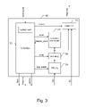
- FIG. 3 is a block diagram of the memory controller of FIG. 1 in one embodiment of the invention.
- FIG. 4 is a flowchart of a method for control logic of the memory controller of FIG. 1 to keep an expected strobe count and a detected strobe count in one embodiment of the invention.
- FIG. 5 is a flowchart of a method for control logic of the memory controller of FIG. 1 to determine whether a strobe error has occurred in one embodiment of the invention.
- FIG. 1 is a block diagram of a data processing system 100 including a memory controller 102 coupled between a memory device 104 and a memory controller client 106 in one embodiment of the invention. Although only one memory device 104 is shown, memory controller 102 may be coupled to additional memory devices.
- Memory controller 102 communicates with memory device 104 through a source synchronous interface while memory controller 102 communicates with memory controller client 106 through a synchronous interface with a system clock.
- memory controller 102 receives a read request from memory controller client 106 and then issues the appropriate read command and address to memory device 104 .
- memory device 104 returns data signals on DQ lines and a data strobe signal on a DQS line.
- DQ and DQS are used to describe the signals and the lines on which the signals travel interchangeably.
- memory device 104 is a dual data rate (DDR) synchronous dynamic random access memory (SDRAM) module that has 72 DQ lines divided into 16 nibbles of 4 DQ lines where each nibble has its own DQS line.
- memory controller 102 and memory controller client 106 can be part of a node controller in a data storage system described in commonly assigned U.S. patent application Ser. No. 09/883,681 filed on Jun. 18, 2001.
- memory device 104 can be the cache memory of the node controller, and memory controller client 106 can be a link interface, a logic engine, or a peripheral component interconnect (PCI) bus interface in the node controller.
- Memory device 104 may be a DDR SDRAM, a DDR2 SDRAM, a DDR3 SDRAM, or a future version of DDR SDRAM.
- FIG. 2 illustrates an exemplary timing diagram of a single data signal DQ and data strobe signal DQS.
- data strobe line DQS Prior to data transmission, data strobe line DQS is maintained at high impedance (also known as hi-Z, tri-stated, or floating).
- memory device 104 pulls data strobe line DQS low to form a preamble. After the preamble, memory device 104 oscillates data strobe signal DQS and provides data signal DQ.
- memory device 104 pulls data strobe line DQS to high impedance to form a postamble.
- Memory controller 102 adds a delay to data strobe signal DQS so it is centered with data signal DQ. Memory controller 102 then captures the values of data signal DQ in response to the delayed data strobe signal DQS.
- FIG. 3 illustrates a block diagram of memory controller 102 in one embodiment of the invention.
- Memory controller 102 includes control logic 302 that manages memory operations.
- Control logic 302 generates the command and the address signals to memory device 104 .
- Control logic 302 also generates control signals to a data strobe gate circuit 304 , a data strobe delay circuit 306 , a data strobe counter circuit 308 , and a read buffer 310 as explained later.
- Control logic 302 may be conventionally implemented with state machines and other control circuitry.
- Gate circuit 304 is coupled to data strobe line DQS. When a control signal DQS_enable is in a first state (e.g., high), gate circuit 304 passes the data strobe signal to delay circuit 306 . When control signal DQS_enable is in a second state (e.g., low), gate circuit 304 blocks the data strobe signal from reaching delay circuit 306 .
- Delay circuit 306 adds a delay to the data strobe signal in order to center it with the data signal.
- Control logic 302 may set delay circuit 306 with the appropriate delay.
- Delay circuit 306 outputs a delayed data strobe signal to strobe counter 308 and read buffer 310 .
- Delayed circuit 306 may be conventionally implemented with a programmable delayed locked loop.
- Counter circuit 308 increments a detected strobe count whenever it detects a transition (either a rising or a falling edge) in the data strobe signal. Counter circuit 308 outputs the detected strobe count to control logic 302 . Control logic 302 may reset counter circuit 308 to clear the detected strobe count. Counter circuit 308 may be conventionally implemented with interconnected flip-flops.
- Read buffer 310 captures the data values on data line DQ in response to the delayed strobe signal, buffers the data values, and then outputs the data values.
- Read buffer 310 may be conventionally implemented as follows. Data inputs of flip-flops are connected to receive data signal DQ. The outputs of a one-hot shift register are connected to the clock inputs of the flip-flops to sequentially clock out the value of data signal DQ in response to the rising and the falling edges of the delayed data strobe signal DQS. Inputs of a multiplexer are connected to the data outputs of the flip-flops. The values of data signal DQ are sequentially selected as the output of the multiplexer by control logic 302 .
- FIG. 4 illustrates a method 400 for control logic 302 to track both an expected strobe count and the detected strobe count in one embodiment of the invention
- FIG. 5 illustrates a method 500 for control logic 302 to report a strobe error to memory controller client 106 in one embodiment of the invention.
- control logic 302 receives a read request from memory controller client 106 .
- the read request specifies the burst length of the data to be read.
- control logic 302 increments the expected strobe count by a number of strobes that corresponds to the burst length of the read request. For example, I number of strobes may correspond to a J-bytes read.
- control logic 302 issues the appropriate read command and address to memory device 104 .
- control logic 302 asserts a high DQS_enable signal to enable gate circuit 304 just after the start of the preamble in the data strobe signal. Control logic 302 does this by asserting DQS_enable X system clock cycles plus a programmable delay after issuing the read command.
- the X system clock cycles correspond to the read latency of memory device 104 .
- the programmable delay is set according to the physical setup, such as the number of memory devices connected to memory controller 102 and the distance from the memory devices to memory controller 102 .
- control logic 302 asserts a low DQS_enable signal just prior to the end of the postamble in the data strobe signal. Control logic 302 does this by asserting DQS_enable low Y system clock cycles plus the programmable delay after asserting DQS_enable high. The Y system clock cycles correspond to the burst length of the requested read. Once gate circuit 304 is disabled, counter circuit 308 no longer receives the delayed data strobe signal and stops to increment the detected strobe count.
- control logic 302 determines if it is free to check for strobe error.
- Control logic 302 is free to check for strobe error when memory controller 102 is idle or when control logic 302 is processing a write request or refreshing.
- memory controller 102 is free to check for error when it is not expecting data strobe signal DQS in response to a read of a memory device. If control logic 302 is free to check for strobe error, then step 502 is followed by step 504 . Otherwise step 502 repeats so that control logic 302 periodically determines to see if it is free to check for strobe error.
- memory controller client 106 can force control logic 302 to idle and check for strobe error.
- control logic 302 reads the detected strobe count from counter circuit 308 .
- Step 504 is followed by step 506 .
- control logic 302 determines if the detected and the expected strobe counts match. If the detected and the expected strobe counts do not match, then step 506 is followed by step 508 . Otherwise step 506 is followed by step 510 .
- control logic 302 reports a data strobe error.
- control logic 302 may report the data strobe error to memory controller client 106 or to other components (hardware or software).
- Step 508 is followed by step 510 .
- control logic 302 clears the detected and the expected strobe counts. Control logic 302 clears the detected strobe count by asserting a Reset signal to counter circuit 308 .
Landscapes
- Engineering & Computer Science (AREA)
- Theoretical Computer Science (AREA)
- Physics & Mathematics (AREA)
- General Engineering & Computer Science (AREA)
- General Physics & Mathematics (AREA)
- Dram (AREA)
Abstract
Description
Claims (13)
Priority Applications (1)
| Application Number | Priority Date | Filing Date | Title |
|---|---|---|---|
| US11/552,107 US7457175B1 (en) | 2006-10-23 | 2006-10-23 | Dual data rate memory strobe checker |
Applications Claiming Priority (1)
| Application Number | Priority Date | Filing Date | Title |
|---|---|---|---|
| US11/552,107 US7457175B1 (en) | 2006-10-23 | 2006-10-23 | Dual data rate memory strobe checker |
Publications (1)
| Publication Number | Publication Date |
|---|---|
| US7457175B1 true US7457175B1 (en) | 2008-11-25 |
Family
ID=40029505
Family Applications (1)
| Application Number | Title | Priority Date | Filing Date |
|---|---|---|---|
| US11/552,107 Expired - Fee Related US7457175B1 (en) | 2006-10-23 | 2006-10-23 | Dual data rate memory strobe checker |
Country Status (1)
| Country | Link |
|---|---|
| US (1) | US7457175B1 (en) |
Cited By (13)
| Publication number | Priority date | Publication date | Assignee | Title |
|---|---|---|---|---|
| US20090161452A1 (en) * | 2007-12-19 | 2009-06-25 | Integrated Device Technology, Inc. | Systems and methods for clean DQS signal generation in source-synchronous DDR2 interface design |
| US20110299347A1 (en) * | 2010-06-04 | 2011-12-08 | Xilinx, Inc. | Dynamic detection of a strobe signal within an integrated circuit |
| WO2013177315A1 (en) * | 2012-05-22 | 2013-11-28 | Advanced Micro Devices, Inc. | Method and apparatus for memory access delay training |
| WO2013164699A3 (en) * | 2012-05-01 | 2014-01-09 | Marvell World Trade Ltd. | Systems and methods for dqs gating |
| US20140145756A1 (en) * | 2012-11-27 | 2014-05-29 | Altera Corporation | Memory interface circuitry with improved timing margins |
| WO2014191838A3 (en) * | 2013-05-28 | 2015-04-09 | Marvell World Trade Ltd. | Systems and methods for dqs gating |
| US9454421B2 (en) | 2013-10-15 | 2016-09-27 | Cypress Semiconductor Corporation | Method for providing read data flow control or error reporting using a read data strobe |
| US9466349B1 (en) * | 2015-06-15 | 2016-10-11 | SK Hynix Inc. | Semiconductor system with training function for a data strobe signal |
| US20170110175A1 (en) * | 2015-10-16 | 2017-04-20 | Samsung Electronics Co., Ltd. | Clean data strobe signal generating circuit in read interface device |
| US10572406B2 (en) | 2016-12-08 | 2020-02-25 | Samsung Electronics Co., Ltd. | Memory controller for receiving differential data strobe signals and application processor having the memory controller |
| US10629255B2 (en) * | 2017-01-09 | 2020-04-21 | Via Alliance Semiconductor Co., Ltd. | Processing system and method for data strobe signal |
| US11127444B1 (en) | 2019-08-20 | 2021-09-21 | Rambus Inc. | Signal receiver with skew-tolerant strobe gating |
| US11493949B2 (en) * | 2020-03-27 | 2022-11-08 | Qualcomm Incorporated | Clocking scheme to receive data |
Citations (4)
| Publication number | Priority date | Publication date | Assignee | Title |
|---|---|---|---|---|
| US6215710B1 (en) * | 1998-10-28 | 2001-04-10 | Hyundai Electronics Industries Co., Ltd. | Apparatus and method for controlling data strobe signal in DDR SDRAM |
| US6940768B2 (en) * | 2003-11-04 | 2005-09-06 | Agere Systems Inc. | Programmable data strobe offset with DLL for double data rate (DDR) RAM memory |
| US7345933B1 (en) * | 2005-01-13 | 2008-03-18 | Marvell Semiconductor Israel Ltd. | Qualified data strobe signal for double data rate memory controller module |
| US7394707B2 (en) * | 2005-06-24 | 2008-07-01 | Lsi Corporation | Programmable data strobe enable architecture for DDR memory applications |
-
2006
- 2006-10-23 US US11/552,107 patent/US7457175B1/en not_active Expired - Fee Related
Patent Citations (4)
| Publication number | Priority date | Publication date | Assignee | Title |
|---|---|---|---|---|
| US6215710B1 (en) * | 1998-10-28 | 2001-04-10 | Hyundai Electronics Industries Co., Ltd. | Apparatus and method for controlling data strobe signal in DDR SDRAM |
| US6940768B2 (en) * | 2003-11-04 | 2005-09-06 | Agere Systems Inc. | Programmable data strobe offset with DLL for double data rate (DDR) RAM memory |
| US7345933B1 (en) * | 2005-01-13 | 2008-03-18 | Marvell Semiconductor Israel Ltd. | Qualified data strobe signal for double data rate memory controller module |
| US7394707B2 (en) * | 2005-06-24 | 2008-07-01 | Lsi Corporation | Programmable data strobe enable architecture for DDR memory applications |
Cited By (25)
| Publication number | Priority date | Publication date | Assignee | Title |
|---|---|---|---|---|
| US7590025B2 (en) * | 2007-12-19 | 2009-09-15 | Integrated Device Technology, Inc. | Systems and methods for clean DQS signal generation in source-synchronous DDR2 interface design |
| US20090161452A1 (en) * | 2007-12-19 | 2009-06-25 | Integrated Device Technology, Inc. | Systems and methods for clean DQS signal generation in source-synchronous DDR2 interface design |
| US20110299347A1 (en) * | 2010-06-04 | 2011-12-08 | Xilinx, Inc. | Dynamic detection of a strobe signal within an integrated circuit |
| US8270235B2 (en) * | 2010-06-04 | 2012-09-18 | Xilinx, Inc. | Dynamic detection of a strobe signal within an integrated circuit |
| WO2013164699A3 (en) * | 2012-05-01 | 2014-01-09 | Marvell World Trade Ltd. | Systems and methods for dqs gating |
| US9285824B2 (en) | 2012-05-01 | 2016-03-15 | Marvell World Trade Ltd. | Systems and methods for DQS gating |
| US8760946B2 (en) | 2012-05-22 | 2014-06-24 | Advanced Micro Devices | Method and apparatus for memory access delay training |
| WO2013177315A1 (en) * | 2012-05-22 | 2013-11-28 | Advanced Micro Devices, Inc. | Method and apparatus for memory access delay training |
| US20140145756A1 (en) * | 2012-11-27 | 2014-05-29 | Altera Corporation | Memory interface circuitry with improved timing margins |
| US9166596B2 (en) * | 2012-11-27 | 2015-10-20 | Altera Corporation | Memory interface circuitry with improved timing margins |
| CN103839573A (en) * | 2012-11-27 | 2014-06-04 | 阿尔特拉公司 | Memory interface circuitry with improved timing margins |
| CN103839573B (en) * | 2012-11-27 | 2017-08-15 | 阿尔特拉公司 | With the memory interface circuit for improving time sequence allowance |
| WO2014191838A3 (en) * | 2013-05-28 | 2015-04-09 | Marvell World Trade Ltd. | Systems and methods for dqs gating |
| US9524255B2 (en) | 2013-05-28 | 2016-12-20 | Marvell World Trade Ltd. | System and method for automatic DQS gating based on counter signal |
| US9454421B2 (en) | 2013-10-15 | 2016-09-27 | Cypress Semiconductor Corporation | Method for providing read data flow control or error reporting using a read data strobe |
| US10120590B2 (en) | 2013-10-15 | 2018-11-06 | Cypress Semiconductor Corporation | Method for providing read data flow control or error reporting using a read data strobe |
| US11010062B2 (en) | 2013-10-15 | 2021-05-18 | Cypress Semiconductor Corporation | Method for providing read data flow control or error reporting using a read data strobe |
| US9466349B1 (en) * | 2015-06-15 | 2016-10-11 | SK Hynix Inc. | Semiconductor system with training function for a data strobe signal |
| US20170110175A1 (en) * | 2015-10-16 | 2017-04-20 | Samsung Electronics Co., Ltd. | Clean data strobe signal generating circuit in read interface device |
| US10147481B2 (en) * | 2015-10-16 | 2018-12-04 | Samsung Electronics Co., Ltd. | Clean data strobe signal generating circuit in read interface device |
| US10572406B2 (en) | 2016-12-08 | 2020-02-25 | Samsung Electronics Co., Ltd. | Memory controller for receiving differential data strobe signals and application processor having the memory controller |
| US10629255B2 (en) * | 2017-01-09 | 2020-04-21 | Via Alliance Semiconductor Co., Ltd. | Processing system and method for data strobe signal |
| US11127444B1 (en) | 2019-08-20 | 2021-09-21 | Rambus Inc. | Signal receiver with skew-tolerant strobe gating |
| US11763865B1 (en) * | 2019-08-20 | 2023-09-19 | Rambus Inc. | Signal receiver with skew-tolerant strobe gating |
| US11493949B2 (en) * | 2020-03-27 | 2022-11-08 | Qualcomm Incorporated | Clocking scheme to receive data |
Similar Documents
| Publication | Publication Date | Title |
|---|---|---|
| US7457175B1 (en) | Dual data rate memory strobe checker | |
| US10482936B2 (en) | Signal training for prevention of metastability due to clocking indeterminacy | |
| US8234422B2 (en) | Interfaces, circuits, and methods for communicating with a double data rate memory device | |
| EP2036090B1 (en) | Synchronous memory read data capture | |
| US10482946B2 (en) | Management of strobe/clock phase tolerances during extended write preambles | |
| US20020184461A1 (en) | Method and apparatus for control calibration of multiple memory modules within a memory channel | |
| US10832760B2 (en) | Systems and methods for improving write preambles in DDR memory devices | |
| US10162406B1 (en) | Systems and methods for frequency mode detection and implementation | |
| CN111837187B (en) | Internal write equalization circuitry | |
| US20210118483A1 (en) | Multi-phase clock division | |
| CN114078503A (en) | Burst clocking based on local command decoding in a memory device | |
| CN110574110B (en) | Dynamic termination edge control | |
| US7590025B2 (en) | Systems and methods for clean DQS signal generation in source-synchronous DDR2 interface design | |
| CN116052739A (en) | Ghost command suppression in a half-frequency memory device | |
| US20230393929A1 (en) | System And Method To Control Memory Error Detection With Automatic Disabling | |
| US20230124182A1 (en) | Systems and methods for centralized address capture circuitry | |
| CN117666942A (en) | Synchronous input buffer control using ripple counter |
Legal Events
| Date | Code | Title | Description |
|---|---|---|---|
| AS | Assignment |
Owner name: 3PARDATA, INC., CALIFORNIA Free format text: ASSIGNMENT OF ASSIGNORS INTEREST;ASSIGNORS:GRIFFITH, DAVID L.;CEKLEOV, MICHEL P.;REEL/FRAME:018425/0191 Effective date: 20061019 |
|
| AS | Assignment |
Owner name: 3PAR INC.,CALIFORNIA Free format text: CHANGE OF NAME;ASSIGNOR:3PARDATA, INC.;REEL/FRAME:020571/0664 Effective date: 20070731 Owner name: 3PAR INC., CALIFORNIA Free format text: CHANGE OF NAME;ASSIGNOR:3PARDATA, INC.;REEL/FRAME:020571/0664 Effective date: 20070731 |
|
| STCF | Information on status: patent grant |
Free format text: PATENTED CASE |
|
| AS | Assignment |
Owner name: HEWLETT-PACKARD DEVELOPMENT COMPANY, L.P., TEXAS Free format text: ASSIGNMENT OF ASSIGNORS INTEREST;ASSIGNOR:3PAR INC.;REEL/FRAME:026250/0322 Effective date: 20110412 |
|
| FPAY | Fee payment |
Year of fee payment: 4 |
|
| AS | Assignment |
Owner name: HEWLETT PACKARD ENTERPRISE DEVELOPMENT LP, TEXAS Free format text: ASSIGNMENT OF ASSIGNORS INTEREST;ASSIGNOR:HEWLETT-PACKARD DEVELOPMENT COMPANY, L.P.;REEL/FRAME:037079/0001 Effective date: 20151027 |
|
| FPAY | Fee payment |
Year of fee payment: 8 |
|
| FEPP | Fee payment procedure |
Free format text: MAINTENANCE FEE REMINDER MAILED (ORIGINAL EVENT CODE: REM.); ENTITY STATUS OF PATENT OWNER: LARGE ENTITY |
|
| LAPS | Lapse for failure to pay maintenance fees |
Free format text: PATENT EXPIRED FOR FAILURE TO PAY MAINTENANCE FEES (ORIGINAL EVENT CODE: EXP.); ENTITY STATUS OF PATENT OWNER: LARGE ENTITY |
|
| STCH | Information on status: patent discontinuation |
Free format text: PATENT EXPIRED DUE TO NONPAYMENT OF MAINTENANCE FEES UNDER 37 CFR 1.362 |
|
| FP | Expired due to failure to pay maintenance fee |
Effective date: 20201125 |