US7453097B2 - Nanowire light emitting device and method of fabricating the same - Google Patents
Nanowire light emitting device and method of fabricating the same Download PDFInfo
- Publication number
- US7453097B2 US7453097B2 US11/100,376 US10037605A US7453097B2 US 7453097 B2 US7453097 B2 US 7453097B2 US 10037605 A US10037605 A US 10037605A US 7453097 B2 US7453097 B2 US 7453097B2
- Authority
- US
- United States
- Prior art keywords
- nanowires
- type doped
- light emitting
- doped portion
- molecules
- Prior art date
- Legal status (The legal status is an assumption and is not a legal conclusion. Google has not performed a legal analysis and makes no representation as to the accuracy of the status listed.)
- Expired - Fee Related, expires
Links
Images


Classifications
-
- H—ELECTRICITY
- H10—SEMICONDUCTOR DEVICES; ELECTRIC SOLID-STATE DEVICES NOT OTHERWISE PROVIDED FOR
- H10D—INORGANIC ELECTRIC SEMICONDUCTOR DEVICES
- H10D62/00—Semiconductor bodies, or regions thereof, of devices having potential barriers
- H10D62/10—Shapes, relative sizes or dispositions of the regions of the semiconductor bodies; Shapes of the semiconductor bodies
-
- H—ELECTRICITY
- H10—SEMICONDUCTOR DEVICES; ELECTRIC SOLID-STATE DEVICES NOT OTHERWISE PROVIDED FOR
- H10H—INORGANIC LIGHT-EMITTING SEMICONDUCTOR DEVICES HAVING POTENTIAL BARRIERS
- H10H20/00—Individual inorganic light-emitting semiconductor devices having potential barriers, e.g. light-emitting diodes [LED]
- H10H20/80—Constructional details
- H10H20/81—Bodies
- H10H20/819—Bodies characterised by their shape, e.g. curved or truncated substrates
- H10H20/821—Bodies characterised by their shape, e.g. curved or truncated substrates of the light-emitting regions, e.g. non-planar junctions
-
- B—PERFORMING OPERATIONS; TRANSPORTING
- B82—NANOTECHNOLOGY
- B82Y—SPECIFIC USES OR APPLICATIONS OF NANOSTRUCTURES; MEASUREMENT OR ANALYSIS OF NANOSTRUCTURES; MANUFACTURE OR TREATMENT OF NANOSTRUCTURES
- B82Y20/00—Nanooptics, e.g. quantum optics or photonic crystals
-
- H—ELECTRICITY
- H10—SEMICONDUCTOR DEVICES; ELECTRIC SOLID-STATE DEVICES NOT OTHERWISE PROVIDED FOR
- H10H—INORGANIC LIGHT-EMITTING SEMICONDUCTOR DEVICES HAVING POTENTIAL BARRIERS
- H10H20/00—Individual inorganic light-emitting semiconductor devices having potential barriers, e.g. light-emitting diodes [LED]
- H10H20/80—Constructional details
- H10H20/81—Bodies
- H10H20/813—Bodies having a plurality of light-emitting regions, e.g. multi-junction LEDs or light-emitting devices having photoluminescent regions within the bodies
-
- B—PERFORMING OPERATIONS; TRANSPORTING
- B82—NANOTECHNOLOGY
- B82Y—SPECIFIC USES OR APPLICATIONS OF NANOSTRUCTURES; MEASUREMENT OR ANALYSIS OF NANOSTRUCTURES; MANUFACTURE OR TREATMENT OF NANOSTRUCTURES
- B82Y10/00—Nanotechnology for information processing, storage or transmission, e.g. quantum computing or single electron logic
-
- H—ELECTRICITY
- H10—SEMICONDUCTOR DEVICES; ELECTRIC SOLID-STATE DEVICES NOT OTHERWISE PROVIDED FOR
- H10H—INORGANIC LIGHT-EMITTING SEMICONDUCTOR DEVICES HAVING POTENTIAL BARRIERS
- H10H20/00—Individual inorganic light-emitting semiconductor devices having potential barriers, e.g. light-emitting diodes [LED]
- H10H20/80—Constructional details
- H10H20/81—Bodies
- H10H20/817—Bodies characterised by the crystal structures or orientations, e.g. polycrystalline, amorphous or porous
- H10H20/818—Bodies characterised by the crystal structures or orientations, e.g. polycrystalline, amorphous or porous within the light-emitting regions
Definitions
- the present invention relates to a nanowire light emitting device and a method of fabricating the same, and more particularly, to a nanowire light emitting device producible at a low manufacturing cost and which can be used for forming a large size device and a method of fabricating the nanowire light emitting device.
- a light emitting diode (LED) using gallium nitride (GaN) is used as a light emitting device.
- GaN gallium nitride
- the GaN-based LED has high light emitting efficiency, it has a mismatch problem with a substrate, thus making it difficult to be used for producing a large size device.
- Japanese Patent Laid-Open Publication No. Hei 10-326888 discloses a light emitting device comprising a nanowire made of silicon and a method of fabricating the light emitting device. After a catalytic layer such as gold is deposited on a substrate, the silicon nanowire is grown from the catalytic layer by flowing silicon tetrachloride (SiCl4) gas into a reactor.
- SiCl4 silicon tetrachloride
- U.S. patent Publication No. 2003/0168964 discloses a nanowire light emitting device having a p-n diode structure.
- the lower portion of the nanowire light emitting device is formed of an n-type nanowire and the upper portion is formed of a p-type nanowire, and the nanowire light emitting device emits light from the junction region of the two portions.
- Other components are added using a vapor phase-liquid phase-solid phase (VLS) method in order to fabricate a nanowire light emitting device having the p-n junction structure.
- VLS vapor phase-liquid phase-solid phase
- the nanowire light emitting device having the p-n junction structure is grown on a catalytic layer, the n-type nanowire and the p-type nanowire are sequentially formed, thus making it difficult to obtain a high quality p-n junction structure.
- the present invention provides a light emitting device having a nanowire structure in which p-type and n-type doped portions of the nanowire are clearly divided by adsorbing doping materials on the surface of the nanowire and a method of fabricating the light emitting device.
- a nanowire light emitting device comprising: a substrate; a first conductive layer formed on the substrate; a plurality of nanowires vertically formed on the first conductive layer, each nanowire having a p-type doped portion and an n-type doped portion separately; a light emitting layer between the p-type doped portion and the n-type doped portion; and a second conductive layer formed on the nanowires, wherein at least one of the p-type doped portion and the n-type doped portion are formed by adsorbing molecules around a corresponding circumference of the nanowires.
- the nanowire light emitting device may further comprise an insulating polymer filling a space between the nanowires on the first conductive layer.
- the light emitting layer may be a boundary surface between the p-type doped portion and the n-type doped portion.
- the light emitting layer may be an undoped intrinsic portion interposed between the p-type doped portion and the n-type doped portion.
- the p-type doped portion may be a portion where molecules having a high electron affinity are adsorbed around a circumference thereof.
- the molecules having a high electron affinity may contain fluorine.
- the molecules containing fluorine may be tetrafluoro-tetracyano-quinodimethane (F4-TCNQ) molecules.
- the n-type doped portion may be a portion where molecules having a low ionization potential are adsorbed around a circumference thereof.
- the molecules having a low ionization potential may be molecules containing at least one metal selected from the group consisting of lithium, copper, and zinc, or organic molecules.
- the molecules may be at least one selected from the group consisting of copper phthalocyanine (CuPc), zinc phthalocyanine (ZnPc), pentacene, and bis(ethylenddithio)tetrathiafulvalene (BEDT-TTF).
- the nanowire may be formed of ZnO.
- a method of fabricating a nanowire light emitting device comprising: forming a first electrode layer on a substrate; forming a plurality of nanowires vertically on the first electrode layer; p-doping or n-doping a lower portion of the nanowires; n-doping or p-doping an upper portion of the nanowires with a different polarity from that of the lower portion of the nanowires; and forming a second electrode layer on the nanowires.
- the p-doping or n-doping of the lower portion of the nanowires may comprise: adsorbing molecules having a high electric affinity or a low ionization potential around a circumference of the nanowires; filling a first insulating polymer between the nanowires on the first electrode layer; and removing the molecules adsorbed on the upper portion of the nanowires by etching the first insulating polymer corresponding to the upper portion of the nanowires.
- the n-doping or p-doping of the upper portion of the nanowires with a different polarity from that of the lower portion of the nanowires may comprise adsorbing molecules having a high electric affinity or a low ionization potential so that the different polarity portion is doped around the circumference of the nanowires exposed on the lower portion of the nanowires.
- the n-doping or p-doping of the upper portion of the nanowires may comprise: forming an undoped intrinsic portion of the nanowires with a predetermined height on the resultant of the p-doping or n-doping of the lower portion of the nanowires; and adsorbing molecules having a high electric affinity or a low ionization potential so that the different polarity portion is doped around the circumference of the nanowires exposed on the intrinsic portion.
- the forming of the intrinsic portion may comprise: forming a second insulating polymer covering the nanowires exposed on the resultant of the p-doping or n-doping of the lower portion of the nanowires; and etching the second insulating polymer to form the intrinsic portion on the upper portion of the nanowires to a predetermined height.
- the forming of the second electrode layer on the nanowires may comprise: etching the third insulating polymer to expose edges of the nanowires; and forming a second conductive layer on the third insulating polymer.
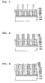
- FIG. 1 is a cross-sectional view of a nanowire light emitting device according to a first exemplary embodiment of the present invention.
- FIG. 2 is a cross-sectional view of a nanowire light emitting device according to a second exemplary embodiment of the present invention.
- FIG. 3 through FIG. 10 are cross-sectional views illustrating a method of fabricating a nanowire light emitting device according to the first exemplary embodiment of the present invention.
- a nanowire light emitting device and a method of fabricating the same according to the present invention will become more apparent by describing in detail exemplary embodiments thereof with reference to the attached drawings.
- FIG. 1 is a cross-sectional view of a nanowire light emitting device according to a first exemplary embodiment of the present invention.
- a conductive layer (a first electrode layer) 110 is formed on a substrate 100 and a plurality of nanowires 120 are vertically formed on the conductive layer 110 .
- An insulating polymer 130 is filled in a space between the nanowires 120 .
- An electrode layer (a second electrode layer) 140 is formed on the nanowires 120 .
- the nanowires 120 are composed of a p-type doped portion 122 , an n-type doped portion 126 , and an intrinsic portion 124 , being a light emitting layer between the p-type doped portion 122 and the n-type doped portion 126 .
- the intrinsic portion is not doped.
- the substrate 100 may be formed of a silicon wafer, a sapphire wafer, or a flat metal film.
- the first electrode layer 110 may be composed of aluminum, gold, or magnesium.
- the second electrode layer 140 may be formed as a transparent electrode layer, for example, an ITO or a p-type doped GaN layer.
- the nanowires 120 may be formed of ZnO, GaN, GaAs, InGaN, CdS, or Si.
- the light emitted from the light emitting device varies according to the material of the nanowires 120 .
- the nanowires are formed of ZnO, ultraviolet rays are emitted.
- the nanowires are formed of Si, infrared rays are emitted.
- the nanowires are formed of GaN, ultraviolet rays or blue light are emitted.
- the nanowires are formed of InGaN, blue light is emitted.
- CdS green light is emitted.
- the nanowires are formed of GaAs, red light is emitted.
- the nanowires may be formed to have a diameter of 20-100 nm and a length of 1 ⁇ m.
- the nanowires have a p-i-n junction structure formed of a p-doped portion 122 , an n-doped portion 126 , and an intrinsic portion 124 .
- the p-type doped portion 122 is a portion in which a p-type doping material is adsorbed around the circumference of the nanowires 120 .
- a molecule having a high electron affinity such as tetrafluoro-tetracyano-quinodimethane (F4-TCNQ), being an electron acceptor molecule, may be used as the p-type doping material. Because the p-type doping material takes away electrons from the surface of the corresponding nanowires 120 , holes are formed on the surface of the portion where the p-type doping material is adsorbed. Thus, the portion becomes the p-type doped portion 122 .
- the n-type doped portion 126 is a portion in which an n-type doping material is adsorbed around the circumference of the nanowires 120 .
- a molecule having a low ionization potential such as an electron donor molecule containing at least one of lithium, zinc, and metal may be used as the n-type doping material.
- copper phthalocyanine (CuPc) zinc phthalocyanine (ZnPc)
- pentacene and bis(ethylenddithio)tetrathiafulvalene (BEDT-TTF) may be used.
- the n-type doping material provides electrons to the surface of the corresponding nanowires 120 , free electrons are formed on the surface of the portion where the n-type doping material is adsorbed. Thus, the portion becomes the n-type doped portion 126 .
- the insulating polymer 130 prevents an electronic contact between the nanowires 120 .
- a photoresist may be used as the insulating polymer 130 .
- the holes of the p-type doped portion 122 and the electrons of the n-type doped portion 126 are reunited in the intrinsic portion 124 when a positive voltage is applied to the first electrode layer 110 connected with the p-type doped portion 122 of the nanowires 120 and a negative voltage is applied to the second electrode layer 140 connected with the n-type doped portion 126 of the nanowires 120 , thus emitting light.
- the light emitted from the intrinsic portion 124 passes through a transparent electrode layer such as the second electrode layer 140 and is emitted to the outside.
- both the p-type doped portion and the n-type doped portion are doped by adsorption of molecules.
- one of the doped portions may be doped by adsorption and the other portion may be doped by conventional ion implantation.
- FIG. 2 is a cross-sectional view of a nanowire light emitting device according to a second exemplary embodiment of the present invention.
- a conductive layer (a first electrode layer) 110 is formed on a substrate 100 and a plurality of nanowires 120 ′ are vertically formed on the conductive layer 110 .
- An insulating polymer 130 is filled in a space between the nanowires 120 ′.
- An electrode layer (a second electrode layer) 140 is formed on the nanowires 120 ′.
- a p-type doped portion 122 and an n-type doped portion 126 are formed in contact with each other in the nanowires 120 ′, and a boundary surface between the p-type doped portion 122 and the n-type portion 126 forms a light emitting layer 128 .
- Such a light emitting structure forms a p-n junction structure in comparison to the p-i-n junction structure of the first exemplary embodiment.
- a light emitting device having the above structure, light is emitted from the light emitting layer 128 when a direct current passes through both ends of the nanowires 120 ′.
- FIG. 3 through FIG. 10 are diagrams illustrating a method of fabricating a nanowire light emitting device according to the first exemplary embodiment of the present invention.
- a conductive layer 210 such as an aluminum layer is deposited on a substrate 200 .
- a plurality of nanowires 220 are formed to have a length of 1 ⁇ m on the aluminum layer 210 by a metal-organic-vapor phase epitaxy (MOVPE) method.
- the nanowires 220 may be fabricated of ZnO using diethyl-zinc (DEZn) and oxygen as a reacting source.
- DEZn diethyl-zinc
- the method of fabricating the nanowires 220 is not limited to the above method, and a conventional vapor phase-liquid phase-solid phase (VLS) method, a self-assembly method, and a method using a metal catalytic layer may also be used.
- VLS vapor phase-liquid phase-solid phase
- a p-type doping material 221 having a high electron affinity such as a F4-TCNQ molecule is doped on a circumference of the nanowires 220 .
- the p doping material 221 takes away electrons from a surface of the nanowires 220 while being adsorbed on the circumference of the nanowires 220 .
- the nanowires 220 is p-doped.
- an insulating high molecule such as a thin photoresist 230 is spin-coated and then fills a space between the p-doped nanowires 220 on the first conductive layer 210 .
- the photoresist 230 and a portion of the p-type doping material 221 are removed by wet etching the photoresist 230 located in the upper portion of the nanowires 220 or by oxygen plasma of the photoresist 230 located in the upper portion of the nanowires 220 .
- the portion of the nanowires in which the remained p-type doping material 221 is formed becomes a p-type doped portion 222 .
- a thin photoresist 231 is spin-coated on the upper portion of the p-doped portion 222 and then fills the space between the nanowires 220 . Then, the photoresist 231 is selectively removed by wet etching or oxygen plasma. Thus the photoresist 231 having a predetermined height is formed on the photoresist 230 . The portion of the nanowires covered with the photoresist 231 is not a doped region and forms an intrinsic portion 224 .
- an n-type doping material 225 is adsorbed on the circumference of the nanowires 220 exposed on the photoresist 231 .
- Molecules having a low ionization potential such as CuPc, ZnPc, pentacene, and BEDT-TTF may be used as the n-type doping material 225 . Because the n-type doping material 225 provides electrons to the surface of the corresponding nanowires 120 , free electrons are formed on the surface of the portion where the n-type doping material is adsorbed. Thus, the portion becomes the n-type doped portion 126 .
- a thin photoresist 232 is spin-coated and then fills the space between the nanowires 220 exposed on the photoresist 231 .
- the photoresist 232 between the nanowires 220 is selectively wet etched or removed by oxygen plasma to expose an upper edge of the n-doped portion 226 .
- a second conductive layer 240 is deposited to cover the exposed nanowires 220 on the photoresist 232 .
- a light emitting device fabricated by the above method has a p-i-n junction structure of FIG. 1 .
- a method of fabricating a light emitting device having a p-n junction structure as shown in FIG. 2 is similar to the above method except for the process of forming an intrinsic portion as shown in FIG. 7 .
- a nanowire light emitting device comprises a homogenous junction, thus having high light emitting efficiency.
- the device can be mass-produced because matching with a substrate is excellent. Also, the device can be directly applied to a flat display because it can be produced with a large size.
Landscapes
- Chemical & Material Sciences (AREA)
- Engineering & Computer Science (AREA)
- Nanotechnology (AREA)
- Physics & Mathematics (AREA)
- Life Sciences & Earth Sciences (AREA)
- Biophysics (AREA)
- Optics & Photonics (AREA)
- Crystallography & Structural Chemistry (AREA)
- Led Devices (AREA)
- Electroluminescent Light Sources (AREA)
- Luminescent Compositions (AREA)
Abstract
Description
Claims (7)
Applications Claiming Priority (2)
| Application Number | Priority Date | Filing Date | Title |
|---|---|---|---|
| KR1020040023803A KR100552707B1 (en) | 2004-04-07 | 2004-04-07 | Nanowire Light Emitting Device and Manufacturing Method Thereof |
| KR10-2004-0023803 | 2004-04-07 |
Publications (2)
| Publication Number | Publication Date |
|---|---|
| US20050224790A1 US20050224790A1 (en) | 2005-10-13 |
| US7453097B2 true US7453097B2 (en) | 2008-11-18 |
Family
ID=35059666
Family Applications (1)
| Application Number | Title | Priority Date | Filing Date |
|---|---|---|---|
| US11/100,376 Expired - Fee Related US7453097B2 (en) | 2004-04-07 | 2005-04-07 | Nanowire light emitting device and method of fabricating the same |
Country Status (4)
| Country | Link |
|---|---|
| US (1) | US7453097B2 (en) |
| JP (1) | JP4319163B2 (en) |
| KR (1) | KR100552707B1 (en) |
| CN (1) | CN100365836C (en) |
Cited By (6)
| Publication number | Priority date | Publication date | Assignee | Title |
|---|---|---|---|---|
| US20090008664A1 (en) * | 2004-04-07 | 2009-01-08 | Samsung Electronics Co., Ltd. | Nanowire light emitting device |
| US20100108131A1 (en) * | 2006-07-27 | 2010-05-06 | International Business Machines Corporation | Techniques for Use of Nanotechnology in Photovoltaics |
| US20140196776A1 (en) * | 2011-05-30 | 2014-07-17 | Lg Innotek Co., Ltd. | Solar cell apparatus and method of fabricating the same |
| US9373602B2 (en) | 2013-08-30 | 2016-06-21 | Samsung Electronics Co., Ltd. | Wire structure and semiconductor device having the same, and method of manufacturing the wire structure |
| US11637219B2 (en) | 2019-04-12 | 2023-04-25 | Google Llc | Monolithic integration of different light emitting structures on a same substrate |
| US20230139185A1 (en) * | 2020-12-10 | 2023-05-04 | Massachusetts Institute Of Technology | Silicon nano light emitting diodes |
Families Citing this family (43)
| Publication number | Priority date | Publication date | Assignee | Title |
|---|---|---|---|---|
| KR100624419B1 (en) * | 2004-04-07 | 2006-09-19 | 삼성전자주식회사 | Nanowire Light Emitting Device and Manufacturing Method Thereof |
| KR100647288B1 (en) * | 2004-09-13 | 2006-11-23 | 삼성전자주식회사 | Nanowire Light Emitting Device and Manufacturing Method Thereof |
| US20060197436A1 (en) * | 2005-03-01 | 2006-09-07 | Sharp Laboratories Of America, Inc. | ZnO nanotip electrode electroluminescence device on silicon substrate |
| JP5324222B2 (en) * | 2005-08-22 | 2013-10-23 | キュー・ワン・ナノシステムズ・インコーポレイテッド | Nanostructure and photovoltaic cell implementing it |
| US7635600B2 (en) * | 2005-11-16 | 2009-12-22 | Sharp Laboratories Of America, Inc. | Photovoltaic structure with a conductive nanowire array electrode |
| EP1791186A1 (en) * | 2005-11-25 | 2007-05-30 | Stormled AB | Light emitting diode and method for manufacturing the same |
| US20070158661A1 (en) * | 2006-01-12 | 2007-07-12 | Rutgers, The State University Of New Jersey | ZnO nanostructure-based light emitting device |
| KR101198763B1 (en) * | 2006-03-23 | 2012-11-12 | 엘지이노텍 주식회사 | Post structure and LED using the structure and method of making the same |
| KR100820182B1 (en) * | 2006-12-06 | 2008-04-08 | 한국전자통신연구원 | Nanowire Device Manufacturing Method Using Nanoimprinting Lithography |
| KR100872271B1 (en) * | 2006-12-15 | 2008-12-05 | 삼성전기주식회사 | Light-Emitting Device Including Nanowire Array |
| US8030664B2 (en) | 2006-12-15 | 2011-10-04 | Samsung Led Co., Ltd. | Light emitting device |
| US8049203B2 (en) | 2006-12-22 | 2011-11-01 | Qunano Ab | Nanoelectronic structure and method of producing such |
| US7663148B2 (en) * | 2006-12-22 | 2010-02-16 | Philips Lumileds Lighting Company, Llc | III-nitride light emitting device with reduced strain light emitting layer |
| JP5453105B2 (en) * | 2006-12-22 | 2014-03-26 | クナノ アーベー | Nanostructured LEDs and devices |
| US20080157354A1 (en) * | 2007-01-03 | 2008-07-03 | Sharp Laboratories Of America, Inc. | Multiple stacked nanostructure arrays and methods for making the same |
| JP2008258297A (en) * | 2007-04-03 | 2008-10-23 | Matsushita Electric Ind Co Ltd | Light emitting element |
| DE102007031600B4 (en) * | 2007-07-06 | 2015-10-15 | Helmholtz-Zentrum Berlin Für Materialien Und Energie Gmbh | Array of vertical UV light-emitting diodes and method for its production |
| CN104392933B (en) | 2007-08-21 | 2017-11-07 | 加州大学评议会 | Nanostructured with high-performance thermoelectric property |
| FR2922685B1 (en) * | 2007-10-22 | 2011-02-25 | Commissariat Energie Atomique | AN OPTOELECTRONIC DEVICE BASED ON NANOWIRES AND CORRESPONDING METHODS |
| CN101497426B (en) * | 2008-02-02 | 2010-12-08 | 中国科学院理化技术研究所 | Preparation method of tetrathiafulvalene molecular base micron and/or nano functional material |
| JP5059695B2 (en) * | 2008-06-17 | 2012-10-24 | 株式会社デンソー | Wire-like structure, method for manufacturing wire-like structure, thermoelectric conversion element, and Peltier element |
| KR100983511B1 (en) * | 2008-09-12 | 2010-09-27 | 주식회사 하이닉스반도체 | Memory device using nanotube or nanowire network and manufacturing method thereof |
| KR101515100B1 (en) * | 2008-10-21 | 2015-04-24 | 삼성전자주식회사 | Light emitting diode and method for manufacturing the same |
| FR2941325B1 (en) * | 2009-01-22 | 2011-04-22 | Commissariat Energie Atomique | METHOD FOR PERFORMING PN HOMOJUNCTION IN NANOSTRUCTURE |
| US20100319759A1 (en) * | 2009-06-22 | 2010-12-23 | John Fisher | Nanostructure and methods of making the same |
| US9202954B2 (en) * | 2010-03-03 | 2015-12-01 | Q1 Nanosystems Corporation | Nanostructure and photovoltaic cell implementing same |
| KR101766715B1 (en) * | 2010-10-25 | 2017-08-23 | 엘지이노텍 주식회사 | Light emitting diode package |
| US9240328B2 (en) | 2010-11-19 | 2016-01-19 | Alphabet Energy, Inc. | Arrays of long nanostructures in semiconductor materials and methods thereof |
| US8736011B2 (en) | 2010-12-03 | 2014-05-27 | Alphabet Energy, Inc. | Low thermal conductivity matrices with embedded nanostructures and methods thereof |
| WO2012088085A1 (en) * | 2010-12-21 | 2012-06-28 | Alphabet Energy, Inc. | Arrays of filled nanostructures with protruding segments and methods thereof |
| US9051175B2 (en) | 2012-03-07 | 2015-06-09 | Alphabet Energy, Inc. | Bulk nano-ribbon and/or nano-porous structures for thermoelectric devices and methods for making the same |
| US9257627B2 (en) | 2012-07-23 | 2016-02-09 | Alphabet Energy, Inc. | Method and structure for thermoelectric unicouple assembly |
| US9082930B1 (en) | 2012-10-25 | 2015-07-14 | Alphabet Energy, Inc. | Nanostructured thermolectric elements and methods of making the same |
| US9082911B2 (en) | 2013-01-28 | 2015-07-14 | Q1 Nanosystems Corporation | Three-dimensional metamaterial device with photovoltaic bristles |
| US9954126B2 (en) | 2013-03-14 | 2018-04-24 | Q1 Nanosystems Corporation | Three-dimensional photovoltaic devices including cavity-containing cores and methods of manufacture |
| US20140264998A1 (en) | 2013-03-14 | 2014-09-18 | Q1 Nanosystems Corporation | Methods for manufacturing three-dimensional metamaterial devices with photovoltaic bristles |
| CN103715325B (en) * | 2013-12-26 | 2016-09-14 | 辽宁师范大学 | The preparation method of single ZnO micro wire homojunction LED |
| US9691849B2 (en) | 2014-04-10 | 2017-06-27 | Alphabet Energy, Inc. | Ultra-long silicon nanostructures, and methods of forming and transferring the same |
| US11233332B2 (en) * | 2017-05-02 | 2022-01-25 | Electronics And Telecommunications Research Institute | Light absorber |
| JP7147132B2 (en) * | 2017-05-31 | 2022-10-05 | セイコーエプソン株式会社 | Light-emitting device, projector, and method for manufacturing light-emitting device |
| KR102118907B1 (en) * | 2018-09-07 | 2020-06-05 | 한양대학교 산학협력단 | Light emitting diode and fabricating method thereof |
| CN113161414B (en) * | 2021-04-29 | 2023-04-14 | 齐鲁工业大学 | A kind of PN microwire preparation method |
| KR102820214B1 (en) * | 2021-04-30 | 2025-06-13 | 삼성디스플레이 주식회사 | Display device |
Citations (14)
| Publication number | Priority date | Publication date | Assignee | Title |
|---|---|---|---|---|
| US3971870A (en) * | 1971-07-27 | 1976-07-27 | Semi-Elements, Inc. | Semiconductor device material |
| US5332910A (en) * | 1991-03-22 | 1994-07-26 | Hitachi, Ltd. | Semiconductor optical device with nanowhiskers |
| JPH06260721A (en) | 1993-03-09 | 1994-09-16 | Hitachi Ltd | Semiconductor laser |
| US20020175408A1 (en) * | 2001-03-30 | 2002-11-28 | The Regents Of The University Of California | Methods of fabricating nanostructures and nanowires and devices fabricated therefrom |
| US20030168964A1 (en) * | 2002-03-11 | 2003-09-11 | Hsing Chen | Nanowire light emitting device and display |
| CN1447629A (en) | 2002-03-26 | 2003-10-08 | 城户淳二 | organic electroluminescent element |
| CN1453884A (en) | 2002-04-25 | 2003-11-05 | 诠兴开发科技股份有限公司 | Nanowire light-emitting element and display device |
| US20040003839A1 (en) * | 2002-07-05 | 2004-01-08 | Curtin Lawrence F. | Nano photovoltaic/solar cells |
| US20040105810A1 (en) * | 2002-09-12 | 2004-06-03 | Zhifen Ren | Metal oxide nanostructures with hierarchical morphology |
| US20050006673A1 (en) * | 2003-04-04 | 2005-01-13 | Btg International Limited | Nanowhiskers with PN junctions, doped nanowhiskers, and methods for preparing them |
| US20050227391A1 (en) * | 2004-04-07 | 2005-10-13 | Samsung Electronics Co., Ltd. | Nanowire light emitting device and method of fabricating the same |
| US20050224780A1 (en) * | 2004-04-07 | 2005-10-13 | Samsung Electronics Co., Ltd. | Nanowire light emitting device |
| US20060207647A1 (en) * | 2005-03-16 | 2006-09-21 | General Electric Company | High efficiency inorganic nanorod-enhanced photovoltaic devices |
| US7254151B2 (en) * | 2002-07-19 | 2007-08-07 | President & Fellows Of Harvard College | Nanoscale coherent optical components |
Family Cites Families (5)
| Publication number | Priority date | Publication date | Assignee | Title |
|---|---|---|---|---|
| US5976957A (en) * | 1996-10-28 | 1999-11-02 | Sony Corporation | Method of making silicon quantum wires on a substrate |
| JP3598373B2 (en) * | 2001-09-03 | 2004-12-08 | 独立行政法人物質・材料研究機構 | Nanostructures joined and regularly arranged on a substrate and a method for producing the same |
| DE20121631U1 (en) * | 2001-11-09 | 2003-06-18 | Friz Biochem GmbH, 82152 Planegg | Molecular electronic component for the construction of nanoelectronic circuits, molecular electronic assembly and electronic circuit |
| US7192533B2 (en) * | 2002-03-28 | 2007-03-20 | Koninklijke Philips Electronics N.V. | Method of manufacturing nanowires and electronic device |
| US6788453B2 (en) * | 2002-05-15 | 2004-09-07 | Yissum Research Development Company Of The Hebrew Univeristy Of Jerusalem | Method for producing inorganic semiconductor nanocrystalline rods and their use |
-
2004
- 2004-04-07 KR KR1020040023803A patent/KR100552707B1/en not_active Expired - Fee Related
-
2005
- 2005-04-07 JP JP2005110941A patent/JP4319163B2/en not_active Expired - Fee Related
- 2005-04-07 US US11/100,376 patent/US7453097B2/en not_active Expired - Fee Related
- 2005-04-07 CN CNB2005100762203A patent/CN100365836C/en not_active Expired - Fee Related
Patent Citations (14)
| Publication number | Priority date | Publication date | Assignee | Title |
|---|---|---|---|---|
| US3971870A (en) * | 1971-07-27 | 1976-07-27 | Semi-Elements, Inc. | Semiconductor device material |
| US5332910A (en) * | 1991-03-22 | 1994-07-26 | Hitachi, Ltd. | Semiconductor optical device with nanowhiskers |
| JPH06260721A (en) | 1993-03-09 | 1994-09-16 | Hitachi Ltd | Semiconductor laser |
| US20020175408A1 (en) * | 2001-03-30 | 2002-11-28 | The Regents Of The University Of California | Methods of fabricating nanostructures and nanowires and devices fabricated therefrom |
| US20030168964A1 (en) * | 2002-03-11 | 2003-09-11 | Hsing Chen | Nanowire light emitting device and display |
| CN1447629A (en) | 2002-03-26 | 2003-10-08 | 城户淳二 | organic electroluminescent element |
| CN1453884A (en) | 2002-04-25 | 2003-11-05 | 诠兴开发科技股份有限公司 | Nanowire light-emitting element and display device |
| US20040003839A1 (en) * | 2002-07-05 | 2004-01-08 | Curtin Lawrence F. | Nano photovoltaic/solar cells |
| US7254151B2 (en) * | 2002-07-19 | 2007-08-07 | President & Fellows Of Harvard College | Nanoscale coherent optical components |
| US20040105810A1 (en) * | 2002-09-12 | 2004-06-03 | Zhifen Ren | Metal oxide nanostructures with hierarchical morphology |
| US20050006673A1 (en) * | 2003-04-04 | 2005-01-13 | Btg International Limited | Nanowhiskers with PN junctions, doped nanowhiskers, and methods for preparing them |
| US20050227391A1 (en) * | 2004-04-07 | 2005-10-13 | Samsung Electronics Co., Ltd. | Nanowire light emitting device and method of fabricating the same |
| US20050224780A1 (en) * | 2004-04-07 | 2005-10-13 | Samsung Electronics Co., Ltd. | Nanowire light emitting device |
| US20060207647A1 (en) * | 2005-03-16 | 2006-09-21 | General Electric Company | High efficiency inorganic nanorod-enhanced photovoltaic devices |
Non-Patent Citations (3)
| Title |
|---|
| Guk, E.G., et al. "Dopant Impurity Diffusion From Polymer Diffusants and its Applications in Semiconductor Device Technology. A Review." Semiconductors. vol. 33 (1999): pp. 265-275. * |
| Ng, Kwok K. Complete Guide to Semiconductor Devices. 2<SUP>nd</SUP>. Ed. Wiley-Interscience: New York. (2002): pp. 405-406. * |
| Nollau, A., et al. "Controlled n-Type Doping of a Molecular Organic Semiconductor: Naphthalenetetracarboxylic dianhydride (NTCDA) Doped With Bis(ethylenedithio)-tetrathiafulvalene (BEDT-TTF)." J. Appl. Phys. vol. 87 (2000): pp. 4340-4343. * |
Cited By (11)
| Publication number | Priority date | Publication date | Assignee | Title |
|---|---|---|---|---|
| US20090008664A1 (en) * | 2004-04-07 | 2009-01-08 | Samsung Electronics Co., Ltd. | Nanowire light emitting device |
| US7919786B2 (en) * | 2004-04-07 | 2011-04-05 | Samsung Electronics Co., Ltd. | Nanowire light emitting device |
| US20100108131A1 (en) * | 2006-07-27 | 2010-05-06 | International Business Machines Corporation | Techniques for Use of Nanotechnology in Photovoltaics |
| US7977690B2 (en) * | 2006-07-27 | 2011-07-12 | International Business Machines Corporation | Techniques for use of nanotechnology in photovoltaics |
| US20140196776A1 (en) * | 2011-05-30 | 2014-07-17 | Lg Innotek Co., Ltd. | Solar cell apparatus and method of fabricating the same |
| US9966486B2 (en) * | 2011-05-30 | 2018-05-08 | Lg Innotek Co., Ltd. | Solar cell apparatus and method of fabricating the same |
| US9373602B2 (en) | 2013-08-30 | 2016-06-21 | Samsung Electronics Co., Ltd. | Wire structure and semiconductor device having the same, and method of manufacturing the wire structure |
| US11637219B2 (en) | 2019-04-12 | 2023-04-25 | Google Llc | Monolithic integration of different light emitting structures on a same substrate |
| US12191418B2 (en) | 2019-04-12 | 2025-01-07 | Google Llc | Monolithic integration of different light emitting structures on a same substrate |
| US20230139185A1 (en) * | 2020-12-10 | 2023-05-04 | Massachusetts Institute Of Technology | Silicon nano light emitting diodes |
| US11756983B2 (en) * | 2020-12-10 | 2023-09-12 | Massachusetts Institute Of Technology | Silicon nano light emitting diodes |
Also Published As
| Publication number | Publication date |
|---|---|
| JP4319163B2 (en) | 2009-08-26 |
| KR100552707B1 (en) | 2006-02-20 |
| CN100365836C (en) | 2008-01-30 |
| CN1691362A (en) | 2005-11-02 |
| JP2005303300A (en) | 2005-10-27 |
| US20050224790A1 (en) | 2005-10-13 |
| KR20050098538A (en) | 2005-10-12 |
Similar Documents
| Publication | Publication Date | Title |
|---|---|---|
| US7453097B2 (en) | Nanowire light emitting device and method of fabricating the same | |
| US7435996B2 (en) | Nanowire light emitting device and method of fabricating the same | |
| US7919786B2 (en) | Nanowire light emitting device | |
| US8664636B2 (en) | Nanostructured device | |
| US9818830B2 (en) | Recessed contact to semiconductor nanowires | |
| US20090189145A1 (en) | Photodetectors, Photovoltaic Devices And Methods Of Making The Same | |
| US8618572B2 (en) | Light-emitting device and method for manufacturing the same | |
| TWI657595B (en) | Optoelectronic semiconductor device | |
| KR102283105B1 (en) | High heat dissipation nanostructure photonic device and method of manuafcturing the same | |
| CN109545994B (en) | Electroluminescent device, manufacturing method thereof and display device | |
| CN114141805A (en) | Nano-LED array without side wall damage and manufacturing method thereof | |
| JP2007103350A (en) | ZnO nanotip electrode electroluminescent device on silicon substrate and method for producing the same | |
| Kim | Kim et a1. |
Legal Events
| Date | Code | Title | Description |
|---|---|---|---|
| AS | Assignment |
Owner name: SAMSUNG ELECTRONICS CO., LTD., KOREA, REPUBLIC OF Free format text: ASSIGNMENT OF ASSIGNORS INTEREST;ASSIGNORS:JIN, YOUNG-GU;LEE, SUNG-HOON;LEE, HYO-SUG;AND OTHERS;REEL/FRAME:016459/0355 Effective date: 20050406 |
|
| FEPP | Fee payment procedure |
Free format text: PAYOR NUMBER ASSIGNED (ORIGINAL EVENT CODE: ASPN); ENTITY STATUS OF PATENT OWNER: LARGE ENTITY |
|
| FEPP | Fee payment procedure |
Free format text: PAYER NUMBER DE-ASSIGNED (ORIGINAL EVENT CODE: RMPN); ENTITY STATUS OF PATENT OWNER: LARGE ENTITY Free format text: PAYOR NUMBER ASSIGNED (ORIGINAL EVENT CODE: ASPN); ENTITY STATUS OF PATENT OWNER: LARGE ENTITY |
|
| FPAY | Fee payment |
Year of fee payment: 4 |
|
| REMI | Maintenance fee reminder mailed | ||
| LAPS | Lapse for failure to pay maintenance fees | ||
| STCH | Information on status: patent discontinuation |
Free format text: PATENT EXPIRED DUE TO NONPAYMENT OF MAINTENANCE FEES UNDER 37 CFR 1.362 |
|
| STCH | Information on status: patent discontinuation |
Free format text: PATENT EXPIRED DUE TO NONPAYMENT OF MAINTENANCE FEES UNDER 37 CFR 1.362 |
|
| FP | Lapsed due to failure to pay maintenance fee |
Effective date: 20161118 |