US7448917B2 - Connector having pin groups with different pin lengths - Google Patents
Connector having pin groups with different pin lengths Download PDFInfo
- Publication number
- US7448917B2 US7448917B2 US11/621,569 US62156907A US7448917B2 US 7448917 B2 US7448917 B2 US 7448917B2 US 62156907 A US62156907 A US 62156907A US 7448917 B2 US7448917 B2 US 7448917B2
- Authority
- US
- United States
- Prior art keywords
- pin
- connector
- group
- providing
- signal transmission
- Prior art date
- Legal status (The legal status is an assumption and is not a legal conclusion. Google has not performed a legal analysis and makes no representation as to the accuracy of the status listed.)
- Expired - Fee Related
Links
- 230000002093 peripheral effect Effects 0.000 claims abstract description 31
- 230000005540 biological transmission Effects 0.000 claims description 20
- 230000008054 signal transmission Effects 0.000 claims description 17
- 230000005236 sound signal Effects 0.000 claims description 13
- 230000002776 aggregation Effects 0.000 claims description 6
- 238000004220 aggregation Methods 0.000 claims description 6
- 230000008878 coupling Effects 0.000 claims 6
- 238000010168 coupling process Methods 0.000 claims 6
- 238000005859 coupling reaction Methods 0.000 claims 6
- 230000008901 benefit Effects 0.000 description 2
- 238000010586 diagram Methods 0.000 description 2
- 238000003780 insertion Methods 0.000 description 2
- 230000037431 insertion Effects 0.000 description 2
- 238000012986 modification Methods 0.000 description 2
- 230000004048 modification Effects 0.000 description 2
Images


Classifications
-
- H—ELECTRICITY
- H01—ELECTRIC ELEMENTS
- H01R—ELECTRICALLY-CONDUCTIVE CONNECTIONS; STRUCTURAL ASSOCIATIONS OF A PLURALITY OF MUTUALLY-INSULATED ELECTRICAL CONNECTING ELEMENTS; COUPLING DEVICES; CURRENT COLLECTORS
- H01R13/00—Details of coupling devices of the kinds covered by groups H01R12/70 or H01R24/00 - H01R33/00
- H01R13/648—Protective earth or shield arrangements on coupling devices, e.g. anti-static shielding
- H01R13/658—High frequency shielding arrangements, e.g. against EMI [Electro-Magnetic Interference] or EMP [Electro-Magnetic Pulse]
- H01R13/6581—Shield structure
- H01R13/6585—Shielding material individually surrounding or interposed between mutually spaced contacts
-
- H—ELECTRICITY
- H01—ELECTRIC ELEMENTS
- H01R—ELECTRICALLY-CONDUCTIVE CONNECTIONS; STRUCTURAL ASSOCIATIONS OF A PLURALITY OF MUTUALLY-INSULATED ELECTRICAL CONNECTING ELEMENTS; COUPLING DEVICES; CURRENT COLLECTORS
- H01R24/00—Two-part coupling devices, or either of their cooperating parts, characterised by their overall structure
- H01R24/60—Contacts spaced along planar side wall transverse to longitudinal axis of engagement
- H01R24/62—Sliding engagements with one side only, e.g. modular jack coupling devices
Definitions
- the present invention relates to a connector. More particularly, the present invention relates to a connector having different pin lengths.
- USB Universal serial bus
- PDA personal digital assistants
- smart phones GPS devices
- music players music players
- game machines the cost and the volumes thereof may be increased if various connectors are to be disposed therein.
- the pin lengths of a connector are the same, the angle of inserting the connector is different when the user habit and the working environment are different.
- Signal misjudgment may be caused if the pin connection sequence in the connector is not consistent, for example, if the pin for transmitting signal is connected before the ground pin, signal misjudgment will be caused due to a lack of ground voltage level.
- the present invention is directed to provide a connector which is suitable for both USB and audio signal transmissions.
- a connector wherein USB pins and audio signal pins are integrated into an insulating layer, so as to integrate the functions of various connectors.
- a connector wherein pins of different lengths are disposed according to different functions so that the connector can be applied to different insertion angles, accordingly the accuracy of signal transmission is improved and signal misjudgment is avoided.
- the present invention provides a connector for connecting a host and a peripheral device.
- the connector includes N pin groups and each of the pin groups has different pin length, wherein N is a positive integer and is greater than or equal to 3.
- the connector includes 5 pin groups, the pin lengths of the pin groups are respectively L 1 ⁇ L 5 .
- L 1 , L 2 , L 3 , L 4 , L 5 are all positive integers, and L 1 >L 2 >L 3 >L 4 >L 5 .
- the present invention provides a connector for connecting a host and a peripheral device.
- the connector includes two ground pins, three audio pins, a power supply pin, three signal pins, and two data pins.
- the length of the ground pins is L 1
- the length of the audio pins is L 2
- the length of the power supply pin is L 3
- the length of the signal pins is L 4
- the length of the data pins is L 5 .
- L 1 , L 2 , L 3 , L 4 , L 5 are all positive integers and L 1 >L 2 >L 3 >L 4 >L 5 .
- the present invention provides a connector for connecting a host and a peripheral device.
- the connector includes an insulating layer having a top surface and a bottom surface and N pin groups respectively disposed on the top surface and the bottom surface, wherein each of the pin groups has different pin length, N is a positive integer and N is greater than or equal to 3.
- the connector includes 5 pin groups, and the pin lengths of the 5 pin groups are respectively L 1 ⁇ L 5 .
- L 1 , L 2 , L 3 , L 4 , L 5 are all positive integers and L 1 >L 2 >L 3 >L 4 >L 5 .
- multiple pins are adopted in the present invention to integrate USB and audio signal transmission interfaces into a connector so that a single connector can perform more functions, accordingly, the number of connectors and the space required by the connectors in an electronic apparatus can be reduced. Meanwhile, pins of different lengths are disposed according to different functions so that the connector can be applied to different insertion angles, accordingly, the accuracy of signal transmission is increased and signal misjudgment is avoided.
- FIG. 1 is a diagram illustrating the pin lengths of a connector according to an embodiment of the present invention.
- FIG. 2 is a cross-sectional view illustrating the structure of a connector according to an embodiment of the present invention.
- FIG. 3 is a cross-sectional view illustrating the major pins of a connector according to an embodiment of the present invention.
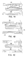
- FIG. 4A is a cross-sectional view of FIG. 3 cut along line A ⁇ A′.
- FIG. 4B is a cross-sectional view of FIG. 3 cut along line B ⁇ B′.
- FIG. 4C is a cross-sectional view of FIG. 3 cut along line C ⁇ C′.
- FIG. 1 is a diagram illustrating the pin lengths of a connector according to an embodiment of the present invention.
- the pin lengths of the connector are classified into 5, which are respectively L 1 ⁇ L 5 .
- the 11 pins P 1 ⁇ P 11 in the present embodiment are classified into 5 pin groups based on the pin lengths L 1 ⁇ L 5 thereof.
- the first pin group is ground pins including pins P 5 and P 10 , which are referred to thereinafter as ground pins P 5 and P 10 , and the pin length thereof is L 1 .
- the second pin group is audio pins including pins P 6 , P 7 , and P 11 , which are referred to thereinafter as audio pins P 6 , P 7 , and P 11 , and the pin length thereof is L 2 .
- the third pin group is power supply pin including only pin P 1 , which is referred to thereinafter as power supply pin P 1 , and the pin length thereof is L 3 .
- the fourth pin group is signal pins including pins P 2 , P 3 , and P 4 , which are referred to thereinafter as signal pins P 2 , P 3 , and P 4 , and the pin length thereof is L 4 .
- the fifth pin group is data pins including pins P 8 and P 9 , which are referred to thereinafter as data pins P 8 and P 9 , and the pin length thereof is L 5 .
- L 1 , L 2 , L 3 , L 4 , and L 5 are all positive integers and L 1 >L 2 >L 3 >L 4 >L 5 .
- the pins P 1 ⁇ P 11 are classified into 5 different lengths, wherein the pin length L 1 of the ground pins P 5 and P 10 is the longest.
- the ground pins P 5 and P 10 always connect the peripheral device and the host first regardless from which direction the user inserts the connector into the host, so that a common ground voltage level can be built up first between the host and the peripheral device to avoid signal misjudgment due to different user habit or working environment.
- FIG. 4C is a cross-sectional view of FIG. 3 cut along line C ⁇ C′
- FIG. 5 is a schematic cross-sectional view for showing the connection between the pins of FIG. 1 and a standard USB interface.
- the data pins P 8 and P 9 are mainly used for providing a digital signal transmission path between the peripheral device and the host, and the pin length L 5 thereof is the shortest.
- the data pin P 9 provides a clock signal transmission path, and the peripheral device can transmit a device data to the host or the device data can be transmitted from the host to the peripheral device along with the clock signal through the data pin P 8 .
- the host determines the type of the peripheral device according to the device data and controls the peripheral device through data transmission.
- the aggregation of the ground pin P 5 , the power supply pin P 1 , and the signal pins P 2 , P 3 , P 4 has the function of connecting a USB interface and the ground pin P 5 , the power supply pin P 1 , and the signal pins P 2 , P 3 , P 4 are disposed on the same surface of the connector.
- the power supply pin P 1 provides the transmission path of the voltage source
- the signal pins P 2 and P 3 provide the transmission path for differential signals in the USB
- the signal pin P 4 is used for determining the master-slave relationship between the host and the peripheral device during signal transmission based on the voltage level thereof.
- FIG. 2 is a cross-sectional view illustrating the structure of a connector according to the present embodiment.
- the pins P 1 ⁇ P 5 are disposed on the same surface of the connector 200 , which is referred to as the top surface of the insulating layer 220 in the present embodiment.
- the pins P 6 ⁇ P 11 are disposed on another side of the connector 200 , which is referred to as the bottom surface of the insulating layer 220 in the present embodiment.
- the outside of the connector 200 is surrounded by a case 210 .
- the insulating layer 220 isolates the pins P 1 ⁇ P 5 and the pins P 6 ⁇ P 11 .
- the connector 200 is connected to a host through a printed circuit board.
- the host can be a PDA, smart cell phone, GPS device, music player, and game machine.
- FIG. 3 is a cross-sectional view illustrating the major pins of a connector according to the present embodiment.
- the cross-sectional view thereof cut along line A ⁇ A′ is as shown in FIG. 4A , wherein the signal pin P 3 is disposed on the top surface of the insulating layer 220 .
- the audio pin P 6 as example, the cross-sectional view thereof cut along line B ⁇ B′ is as shown in FIG. 4B , wherein the ground pin P 5 and the audio pin P 6 are respectively disposed on the top and bottom surface of the insulating layer 220 .
- the ground pin P 5 is closer to the opening of the case 210 than the audio pin P 6 , so that the ground pin P 5 can first come into contact with the corresponding pin of the socket when the connector 200 is connected to the socket.
- the data pin P 8 as example, the cross-sectional view thereof cut along line C ⁇ C′ is as shown in FIG. 4C , wherein the data pin P 8 is disposed on the bottom surface of the insulating layer 220 .
- the aggregation of the ground pin P 5 , the power supply pin P 1 , and the signal pins P 2 , P 3 , P 4 has the function of connecting a standard USB interface 300 (shown in FIG. 5 ) and also the ground pin P 5 , the power supply pin P 1 , and the signal pins P 2 , P 3 , P 4 are disposed on the same surface of the connector.
- the power supply pin P 1 provides the transmission path of the voltage source
- the signal pins P 2 and P 3 provide the transmission path for differential signals in the USB
- the signal pin P 4 is used for determining the master-slave relationship between the host and the peripheral device during signal transmission based on the voltage level thereof.
- pin functions of the present invention are not limited thereto.
- the applications of the present invention in connectors of different pin functions or transmission interfaces can be easily understood based on the present disclosure by those having ordinary knowledge in the art, therefore will not be described herein.
- pins of different lengths are used for different pin functions so that signal misjudgment due to different user habit or working environment can be effectively avoided.
- the functions of various connectors can be integrated into one single connector so that the space and design cost of hand-held electronic devices can be effectively reduced.
Landscapes
- Details Of Connecting Devices For Male And Female Coupling (AREA)
- Coupling Device And Connection With Printed Circuit (AREA)
Abstract
Description
Claims (20)
Applications Claiming Priority (2)
| Application Number | Priority Date | Filing Date | Title |
|---|---|---|---|
| TW095109409A TWI304283B (en) | 2006-03-20 | 2006-03-20 | Connector |
| TW95109409 | 2006-03-20 |
Publications (2)
| Publication Number | Publication Date |
|---|---|
| US20070218725A1 US20070218725A1 (en) | 2007-09-20 |
| US7448917B2 true US7448917B2 (en) | 2008-11-11 |
Family
ID=38518465
Family Applications (1)
| Application Number | Title | Priority Date | Filing Date |
|---|---|---|---|
| US11/621,569 Expired - Fee Related US7448917B2 (en) | 2006-03-20 | 2007-01-10 | Connector having pin groups with different pin lengths |
Country Status (2)
| Country | Link |
|---|---|
| US (1) | US7448917B2 (en) |
| TW (1) | TWI304283B (en) |
Cited By (10)
| Publication number | Priority date | Publication date | Assignee | Title |
|---|---|---|---|---|
| US20070083619A1 (en) * | 2004-03-31 | 2007-04-12 | Sung-Chung Chen | Interface switch system |
| US20070243767A1 (en) * | 2004-03-31 | 2007-10-18 | Aten International Co., Ltd. | Electrical connector |
| US20080180032A1 (en) * | 2007-01-30 | 2008-07-31 | Surefire Llc | Flashlight with multistage switch and ARC lamp operation sensor |
| US7625236B1 (en) * | 2008-06-20 | 2009-12-01 | Hon Hai Precision Ind. Co., Ltd. | Electrical connector having reduced size |
| US20110294359A1 (en) * | 2010-05-26 | 2011-12-01 | Samsung Electronics Co., Ltd. | Connector and interface device |
| US8110760B2 (en) | 2006-04-20 | 2012-02-07 | Streamlight, Inc. | Electrical switch having plural switching elements, as for controlling a flashlight |
| US20150205337A1 (en) * | 2013-06-26 | 2015-07-23 | Huizhou Tcl Mobile Communication Co., Ltd. | Communication module and terminal for implementing hot plug |
| US10063011B2 (en) | 2015-03-04 | 2018-08-28 | Hewlett Packard Enterprise Development Lp | Multiple pins of different lengths corresponding to different data signaling rates |
| TWI776289B (en) * | 2011-03-31 | 2022-09-01 | 捷利知產股份有限公司 | Electronic device with double-sided electrical connection structure switching with locking structure |
| US12224530B2 (en) | 2021-04-01 | 2025-02-11 | Asustek Computer Inc. | Connector assembly of supporting forward and reverse insertion function, and female connector |
Families Citing this family (7)
| Publication number | Priority date | Publication date | Assignee | Title |
|---|---|---|---|---|
| US7670181B2 (en) * | 2006-03-20 | 2010-03-02 | Htc Corporation | Connector for first and second joints having different pin quantities, electronic apparatus with connector and combination |
| CN100490258C (en) * | 2006-05-24 | 2009-05-20 | 宏达国际电子股份有限公司 | Connector for sharing first type connector and second type connector with different pin numbers |
| TWI396348B (en) * | 2007-11-26 | 2013-05-11 | Htc Corp | Connector, connection detection method and adapter using the same |
| CN102750215A (en) * | 2011-04-22 | 2012-10-24 | 鸿富锦精密工业(深圳)有限公司 | Detection device of output signals of SAS (Serial Attached Small Computer System Interface) |
| CN102955728A (en) * | 2011-08-17 | 2013-03-06 | 鸿富锦精密工业(深圳)有限公司 | SAS (serial attached small computer system interface) output signal detection device |
| CN103327656B (en) * | 2013-06-26 | 2016-11-16 | 惠州Tcl移动通信有限公司 | Communication module and portable terminal |
| US10361511B1 (en) * | 2018-06-27 | 2019-07-23 | Western Digital Technologies, Inc. | Removal delay feature for removably connected devices |
Citations (4)
| Publication number | Priority date | Publication date | Assignee | Title |
|---|---|---|---|---|
| US5387114A (en) * | 1993-07-22 | 1995-02-07 | Molex Incorporated | Electrical connector with means for altering circuit characteristics |
| US6347962B1 (en) * | 2001-01-30 | 2002-02-19 | Tyco Electronics Corporation | Connector assembly with multi-contact ground shields |
| US6843686B2 (en) * | 2002-04-26 | 2005-01-18 | Honda Tsushin Kogyo Co., Ltd. | High-frequency electric connector having no ground terminals |
| US6945824B1 (en) | 2004-08-24 | 2005-09-20 | Cheng Uei Precision Industry Co., Ltd. | Connector assembly |
-
2006
- 2006-03-20 TW TW095109409A patent/TWI304283B/en not_active IP Right Cessation
-
2007
- 2007-01-10 US US11/621,569 patent/US7448917B2/en not_active Expired - Fee Related
Patent Citations (4)
| Publication number | Priority date | Publication date | Assignee | Title |
|---|---|---|---|---|
| US5387114A (en) * | 1993-07-22 | 1995-02-07 | Molex Incorporated | Electrical connector with means for altering circuit characteristics |
| US6347962B1 (en) * | 2001-01-30 | 2002-02-19 | Tyco Electronics Corporation | Connector assembly with multi-contact ground shields |
| US6843686B2 (en) * | 2002-04-26 | 2005-01-18 | Honda Tsushin Kogyo Co., Ltd. | High-frequency electric connector having no ground terminals |
| US6945824B1 (en) | 2004-08-24 | 2005-09-20 | Cheng Uei Precision Industry Co., Ltd. | Connector assembly |
Cited By (17)
| Publication number | Priority date | Publication date | Assignee | Title |
|---|---|---|---|---|
| US20070243767A1 (en) * | 2004-03-31 | 2007-10-18 | Aten International Co., Ltd. | Electrical connector |
| US7585176B2 (en) * | 2004-03-31 | 2009-09-08 | Aten International Co., Ltd. | Connector encompassing 15-pin high density D-SUB pinout having additional pin capacity |
| US7774523B2 (en) | 2004-03-31 | 2010-08-10 | Aten International Co., Ltd. | Interface switch system for simultaneously connecting multiple I/O devices |
| US20070083619A1 (en) * | 2004-03-31 | 2007-04-12 | Sung-Chung Chen | Interface switch system |
| US8662701B2 (en) | 2006-04-20 | 2014-03-04 | Streamlight, Inc. | Flashlight having a controller providing programmable operating states |
| US8110760B2 (en) | 2006-04-20 | 2012-02-07 | Streamlight, Inc. | Electrical switch having plural switching elements, as for controlling a flashlight |
| US8360598B2 (en) | 2006-04-20 | 2013-01-29 | Streamlight, Inc. | Flashlight having a switch for programming a controller |
| US20080180032A1 (en) * | 2007-01-30 | 2008-07-31 | Surefire Llc | Flashlight with multistage switch and ARC lamp operation sensor |
| US7549765B2 (en) * | 2007-01-30 | 2009-06-23 | Surefire, Llc | Flashlight with multistage switch and ARC lamp operation sensor |
| US7625236B1 (en) * | 2008-06-20 | 2009-12-01 | Hon Hai Precision Ind. Co., Ltd. | Electrical connector having reduced size |
| US20090318024A1 (en) * | 2008-06-20 | 2009-12-24 | Hon Hai Precision Ind. Co., Ltd. | Electrical connector having reduced size |
| US20110294359A1 (en) * | 2010-05-26 | 2011-12-01 | Samsung Electronics Co., Ltd. | Connector and interface device |
| TWI776289B (en) * | 2011-03-31 | 2022-09-01 | 捷利知產股份有限公司 | Electronic device with double-sided electrical connection structure switching with locking structure |
| US20150205337A1 (en) * | 2013-06-26 | 2015-07-23 | Huizhou Tcl Mobile Communication Co., Ltd. | Communication module and terminal for implementing hot plug |
| US9588561B2 (en) * | 2013-06-26 | 2017-03-07 | Huizhou TCL Mobile Communications Co., Ltd. | Communication module and terminal for implementing hot plug |
| US10063011B2 (en) | 2015-03-04 | 2018-08-28 | Hewlett Packard Enterprise Development Lp | Multiple pins of different lengths corresponding to different data signaling rates |
| US12224530B2 (en) | 2021-04-01 | 2025-02-11 | Asustek Computer Inc. | Connector assembly of supporting forward and reverse insertion function, and female connector |
Also Published As
| Publication number | Publication date |
|---|---|
| US20070218725A1 (en) | 2007-09-20 |
| TW200737612A (en) | 2007-10-01 |
| TWI304283B (en) | 2008-12-11 |
Similar Documents
| Publication | Publication Date | Title |
|---|---|---|
| US7448917B2 (en) | Connector having pin groups with different pin lengths | |
| EP1860739B1 (en) | Connector with contacts of different lengths | |
| US7427214B2 (en) | Compatible connector for first and second joints having different pin quantities | |
| US7544089B2 (en) | Adapter for USB and audio interface | |
| CN104620567B (en) | System and method for detecting ground and microphone input contacts in an audio plug | |
| US7670181B2 (en) | Connector for first and second joints having different pin quantities, electronic apparatus with connector and combination | |
| CN103368014B (en) | Electrical Connectors and Handheld Electronic Devices | |
| CN105867874A (en) | A user device | |
| US20210351601A1 (en) | Wireless sound output device with charging function | |
| US20140307376A1 (en) | Transmittal system and connection device | |
| US8976510B2 (en) | Cable assembly and electronic device | |
| US8111207B2 (en) | Antenna structure and related expansion card and computer apparatus | |
| US8364976B2 (en) | Pass-through adapter with crypto ignition key (CIK) functionality | |
| CN205319383U (en) | Improved connector | |
| US20130065448A1 (en) | Electronic connector | |
| US20080274647A1 (en) | Usb Data-Audio Signal Multiplexing Transmission Line | |
| TWI823122B (en) | USB Type-C MALE CONNECTOR | |
| EP1860746B1 (en) | Compatible connector for first and second joints having different pin quantities | |
| KR20090042375A (en) | USB plug, AV socket for USB plug and USB connector device having same | |
| US20110294310A1 (en) | Memory card and memory card holding structure | |
| CN106785532A (en) | Composite connector | |
| CN202424706U (en) | Wireless transmission device with external antenna | |
| KR101013671B1 (en) | Connector to connect receptacle and USB port of portable terminal | |
| KR200411207Y1 (en) | Multi interface port | |
| KR100839555B1 (en) | USSR memory for multimedia and its control method |
Legal Events
| Date | Code | Title | Description |
|---|---|---|---|
| AS | Assignment |
Owner name: HIGH TECH COMPUTER, CORP., TAIWAN Free format text: ASSIGNMENT OF ASSIGNORS INTEREST;ASSIGNORS:LIAO, YU-JING;LIN, YAO-CHUNG;CHENG, YI-TSUNG;AND OTHERS;REEL/FRAME:018750/0054 Effective date: 20060605 |
|
| AS | Assignment |
Owner name: HTC CORPORATION, TAIWAN Free format text: CHANGE OF NAME;ASSIGNOR:HIGH TECH COMPUTER, CORP.;REEL/FRAME:021575/0029 Effective date: 20080613 |
|
| STCF | Information on status: patent grant |
Free format text: PATENTED CASE |
|
| FPAY | Fee payment |
Year of fee payment: 4 |
|
| FPAY | Fee payment |
Year of fee payment: 8 |
|
| FEPP | Fee payment procedure |
Free format text: MAINTENANCE FEE REMINDER MAILED (ORIGINAL EVENT CODE: REM.); ENTITY STATUS OF PATENT OWNER: LARGE ENTITY |
|
| LAPS | Lapse for failure to pay maintenance fees |
Free format text: PATENT EXPIRED FOR FAILURE TO PAY MAINTENANCE FEES (ORIGINAL EVENT CODE: EXP.); ENTITY STATUS OF PATENT OWNER: LARGE ENTITY |
|
| STCH | Information on status: patent discontinuation |
Free format text: PATENT EXPIRED DUE TO NONPAYMENT OF MAINTENANCE FEES UNDER 37 CFR 1.362 |
|
| FP | Lapsed due to failure to pay maintenance fee |
Effective date: 20201111 |