US7435361B2 - Conductive compositions and processes for use in the manufacture of semiconductor devices - Google Patents
Conductive compositions and processes for use in the manufacture of semiconductor devices Download PDFInfo
- Publication number
- US7435361B2 US7435361B2 US11/106,259 US10625905A US7435361B2 US 7435361 B2 US7435361 B2 US 7435361B2 US 10625905 A US10625905 A US 10625905A US 7435361 B2 US7435361 B2 US 7435361B2
- Authority
- US
- United States
- Prior art keywords
- composition
- glass
- thick film
- zno
- metal
- Prior art date
- Legal status (The legal status is an assumption and is not a legal conclusion. Google has not performed a legal analysis and makes no representation as to the accuracy of the status listed.)
- Expired - Fee Related, expires
Links
- AZHQQSSDJBLSPU-UHFFFAOYSA-N O=[Ce]=O.O=[Co].O=[Cr](=O)(=O)[Cr].O=[Cr][Co][Fe].O=[Cu][Cu].O=[Fe].O=[Gd].O=[Mn].O=[Mn].O=[Mn]=O.O=[Mo](=O)=O.O=[Ru](=O)(=O)[Cu].O=[Ru]=O.O=[Sn]=O.O=[Sn]=O.O=[Ti]=O.O=[W](=O)=O.O=[Zn].O=[Zr]=O Chemical compound O=[Ce]=O.O=[Co].O=[Cr](=O)(=O)[Cr].O=[Cr][Co][Fe].O=[Cu][Cu].O=[Fe].O=[Gd].O=[Mn].O=[Mn].O=[Mn]=O.O=[Mo](=O)=O.O=[Ru](=O)(=O)[Cu].O=[Ru]=O.O=[Sn]=O.O=[Sn]=O.O=[Ti]=O.O=[W](=O)=O.O=[Zn].O=[Zr]=O AZHQQSSDJBLSPU-UHFFFAOYSA-N 0.000 description 1
- RJOABUGTIRFFNM-UHFFFAOYSA-N O=[Zn].O=[Zn].O=[Zn].O=[Zn].O=[Zn].[V][V][V][V][V][V][V][V][V][V][V][V][V][V][V][V][V][V][V][V][V][V][V][V][V][V][V][V][V][V][V][V][V][V][V][V][V][V][V][V][V][V][V][V][V][V][V][V][V][V][V][V][V][V][V][V][V][V][V][V][V][V][V][V][V][V][V][V][V][V][V][V][V][V][V][V][V][V][V][V][V][V][V][V][V][V][V][V][V][V][V][V][V][V][V][V][V][V][V][V][V][V][V][V][V][V][V][V][V][V][V][V][V][V][V][V][V][V][V][V][V][V][V][V][V][V][V][V][V][V][V][V][V][V][V][V][V][V][V][V][V][V][V]P([V])[V] Chemical compound O=[Zn].O=[Zn].O=[Zn].O=[Zn].O=[Zn].[V][V][V][V][V][V][V][V][V][V][V][V][V][V][V][V][V][V][V][V][V][V][V][V][V][V][V][V][V][V][V][V][V][V][V][V][V][V][V][V][V][V][V][V][V][V][V][V][V][V][V][V][V][V][V][V][V][V][V][V][V][V][V][V][V][V][V][V][V][V][V][V][V][V][V][V][V][V][V][V][V][V][V][V][V][V][V][V][V][V][V][V][V][V][V][V][V][V][V][V][V][V][V][V][V][V][V][V][V][V][V][V][V][V][V][V][V][V][V][V][V][V][V][V][V][V][V][V][V][V][V][V][V][V][V][V][V][V][V][V][V][V][V]P([V])[V] RJOABUGTIRFFNM-UHFFFAOYSA-N 0.000 description 1
- QYEGVGMKHFXVEZ-UHFFFAOYSA-N [Zn].[Zn].[Zn] Chemical compound [Zn].[Zn].[Zn] QYEGVGMKHFXVEZ-UHFFFAOYSA-N 0.000 description 1
Images

Classifications
-
- H—ELECTRICITY
- H10—SEMICONDUCTOR DEVICES; ELECTRIC SOLID-STATE DEVICES NOT OTHERWISE PROVIDED FOR
- H10F—INORGANIC SEMICONDUCTOR DEVICES SENSITIVE TO INFRARED RADIATION, LIGHT, ELECTROMAGNETIC RADIATION OF SHORTER WAVELENGTH OR CORPUSCULAR RADIATION
- H10F10/00—Individual photovoltaic cells, e.g. solar cells
-
- H—ELECTRICITY
- H10—SEMICONDUCTOR DEVICES; ELECTRIC SOLID-STATE DEVICES NOT OTHERWISE PROVIDED FOR
- H10F—INORGANIC SEMICONDUCTOR DEVICES SENSITIVE TO INFRARED RADIATION, LIGHT, ELECTROMAGNETIC RADIATION OF SHORTER WAVELENGTH OR CORPUSCULAR RADIATION
- H10F77/00—Constructional details of devices covered by this subclass
- H10F77/20—Electrodes
- H10F77/206—Electrodes for devices having potential barriers
-
- C—CHEMISTRY; METALLURGY
- C03—GLASS; MINERAL OR SLAG WOOL
- C03C—CHEMICAL COMPOSITION OF GLASSES, GLAZES OR VITREOUS ENAMELS; SURFACE TREATMENT OF GLASS; SURFACE TREATMENT OF FIBRES OR FILAMENTS MADE FROM GLASS, MINERALS OR SLAGS; JOINING GLASS TO GLASS OR OTHER MATERIALS
- C03C8/00—Enamels; Glazes; Fusion seal compositions being frit compositions having non-frit additions
- C03C8/02—Frit compositions, i.e. in a powdered or comminuted form
- C03C8/04—Frit compositions, i.e. in a powdered or comminuted form containing zinc
-
- C—CHEMISTRY; METALLURGY
- C03—GLASS; MINERAL OR SLAG WOOL
- C03C—CHEMICAL COMPOSITION OF GLASSES, GLAZES OR VITREOUS ENAMELS; SURFACE TREATMENT OF GLASS; SURFACE TREATMENT OF FIBRES OR FILAMENTS MADE FROM GLASS, MINERALS OR SLAGS; JOINING GLASS TO GLASS OR OTHER MATERIALS
- C03C8/00—Enamels; Glazes; Fusion seal compositions being frit compositions having non-frit additions
- C03C8/02—Frit compositions, i.e. in a powdered or comminuted form
- C03C8/06—Frit compositions, i.e. in a powdered or comminuted form containing halogen
-
- C—CHEMISTRY; METALLURGY
- C03—GLASS; MINERAL OR SLAG WOOL
- C03C—CHEMICAL COMPOSITION OF GLASSES, GLAZES OR VITREOUS ENAMELS; SURFACE TREATMENT OF GLASS; SURFACE TREATMENT OF FIBRES OR FILAMENTS MADE FROM GLASS, MINERALS OR SLAGS; JOINING GLASS TO GLASS OR OTHER MATERIALS
- C03C8/00—Enamels; Glazes; Fusion seal compositions being frit compositions having non-frit additions
- C03C8/14—Glass frit mixtures having non-frit additions, e.g. opacifiers, colorants, mill-additions
- C03C8/18—Glass frit mixtures having non-frit additions, e.g. opacifiers, colorants, mill-additions containing free metals
-
- H—ELECTRICITY
- H01—ELECTRIC ELEMENTS
- H01B—CABLES; CONDUCTORS; INSULATORS; SELECTION OF MATERIALS FOR THEIR CONDUCTIVE, INSULATING OR DIELECTRIC PROPERTIES
- H01B1/00—Conductors or conductive bodies characterised by the conductive materials; Selection of materials as conductors
- H01B1/20—Conductive material dispersed in non-conductive organic material
- H01B1/22—Conductive material dispersed in non-conductive organic material the conductive material comprising metals or alloys
-
- H—ELECTRICITY
- H10—SEMICONDUCTOR DEVICES; ELECTRIC SOLID-STATE DEVICES NOT OTHERWISE PROVIDED FOR
- H10F—INORGANIC SEMICONDUCTOR DEVICES SENSITIVE TO INFRARED RADIATION, LIGHT, ELECTROMAGNETIC RADIATION OF SHORTER WAVELENGTH OR CORPUSCULAR RADIATION
- H10F77/00—Constructional details of devices covered by this subclass
- H10F77/20—Electrodes
- H10F77/206—Electrodes for devices having potential barriers
- H10F77/211—Electrodes for devices having potential barriers for photovoltaic cells
-
- H—ELECTRICITY
- H05—ELECTRIC TECHNIQUES NOT OTHERWISE PROVIDED FOR
- H05K—PRINTED CIRCUITS; CASINGS OR CONSTRUCTIONAL DETAILS OF ELECTRIC APPARATUS; MANUFACTURE OF ASSEMBLAGES OF ELECTRICAL COMPONENTS
- H05K1/00—Printed circuits
- H05K1/02—Details
- H05K1/09—Use of materials for the conductive, e.g. metallic pattern
- H05K1/092—Dispersed materials, e.g. conductive pastes or inks
-
- Y—GENERAL TAGGING OF NEW TECHNOLOGICAL DEVELOPMENTS; GENERAL TAGGING OF CROSS-SECTIONAL TECHNOLOGIES SPANNING OVER SEVERAL SECTIONS OF THE IPC; TECHNICAL SUBJECTS COVERED BY FORMER USPC CROSS-REFERENCE ART COLLECTIONS [XRACs] AND DIGESTS
- Y02—TECHNOLOGIES OR APPLICATIONS FOR MITIGATION OR ADAPTATION AGAINST CLIMATE CHANGE
- Y02E—REDUCTION OF GREENHOUSE GAS [GHG] EMISSIONS, RELATED TO ENERGY GENERATION, TRANSMISSION OR DISTRIBUTION
- Y02E10/00—Energy generation through renewable energy sources
- Y02E10/50—Photovoltaic [PV] energy
Definitions
- This invention is directed primarily to a silicon semiconductor device. In particular, it is directed to a conductive silver paste for use in the front side of a solar cell device.
- the present invention can be applied to a broad range of semiconductor devices, although it is especially effective in light-receiving elements such as photodiodes and solar cells.
- the background of the invention is described below with reference to solar cells as a specific example of the prior art.
- a conventional solar cell structure with a p-type base has a negative electrode that is typically on the front-side or sun side of the cell and a positive electrode on the backside. It is well-known that radiation of an appropriate wavelength falling on a p-n junction of a semiconductor body serves as a source of external energy to generate hole-electron pairs in that body. Because of the potential difference which exists at a p-n junction, holes and electrons move across the junction in opposite directions and thereby give rise to flow of an electric current that is capable of delivering power to an external circuit. Most solar cells are in the form of a silicon wafer that has been metallized, i.e., provided with metal contacts that are electrically conductive.
- FIG. 1 shows a p-type silicon substrate, 10 .
- an n-type diffusion layer, 20 of the reverse conductivity type is formed by the thermal diffusion of phosphorus (P) or the like.
- Phosphorus oxychloride (POCl 3 ) is commonly used as the phosphorus diffusion source.
- the diffusion layer, 20 is formed over the entire surface of the silicon substrate, 10 .
- This diffusion layer has a sheet resistivity on the order of several tens of ohms per square ( ⁇ / ⁇ ), and a thickness of about 0.3 to 0.5 ⁇ m.
- the diffusion layer, 20 After protecting one surface of this diffusion layer with a resist or the like, as shown in FIG. 1( c ), the diffusion layer, 20 , is removed from most surfaces by etching so that it remains only on one main surface. The resist is then removed using an organic solvent or the like.
- a silicon nitride film, 30 is formed as an anti-reflection coating on the n-type diffusion layer, 20 , to a thickness of about 700 to 900 ⁇ in the manner shown in FIG. 1( d ) by a process such as plasma chemical vapor deposition (CVD).
- CVD plasma chemical vapor deposition
- a silver paste, 500 for the front electrode is screen printed then dried over the silicon nitride film, 30 .
- a backside silver or silver/aluminum paste, 70 , and an aluminum paste, 60 are then screen printed and successively dried on the backside of the substrate. Firing is then carried out in an infrared furnace at a temperature range of approximately 700° C. to 975° C. for a period of from several minutes to several tens of minutes.
- aluminum diffuses from the aluminum paste into the silicon substrate, 10 , as a dopant during firing, forming a p+ layer, 40 , containing a high concentration of aluminum dopant.
- This layer is generally called the back surface field (BSF) layer, and helps to improve the energy conversion efficiency of the solar cell.
- BSF back surface field
- the aluminum paste is transformed by firing from a dried state, 60 , to an aluminum back electrode, 61 .
- the backside silver or silver/aluminum paste, 70 is fired at the same time, becoming a silver or silver/aluminum back electrode, 71 .
- the aluminum electrode accounts for most areas of the back electrode, owing in part to the need to form a p+ layer, 40 . Because soldering to an aluminum electrode is impossible, a silver back electrode is formed over portions of the back side as an electrode for interconnecting solar cells by means of copper ribbon or the like.
- the front electrode-forming silver paste, 500 sinters and penetrates through the silicon nitride film, 30 , during firing, and is thereby able to electrically contact the n-type layer, 20 .
- This type of process is generally called “fire through.” This fired through state is apparent in layer 501 of FIG. 1( f ).
- JP-A 2001-313400 to Shuichi et al. teaches a solar cell which is obtained by forming, on one main surface of a semiconductor substrate, regions that exhibit the other type of conductivity and forming an antireflection coating on this main surface of the semiconductor substrate.
- the resulting solar cell has an electrode material coated over the antireflection coating and fired.
- the electrode material includes, for example, lead, boron and silicon, and additionally contains, in a glass frit having a softening point of about 300 to 600° C., and one or more powders from among titanium, bismuth, cobalt, zinc, zirconium, iron, and chromium.
- U.S. Pat. No. 4,737,197 to Nagahara et al. discloses a solar cell including a semiconductor substrate, a diffused layer provided in the semiconductor substrate by diffusion of dopant impurities, and a contact made of metal paste formed on the diffusion layer.
- the metal paste includes metal powder, which functions as the main contact material, glass frits, an organic binder, a solvent, and an element belonging to the fifth group of the periodic table.
- compositions which are Pb-free While at the same time maintaining electrical performance.
- the present inventors create a novel composition and method of manufacturing a semiconductor device which provides such a Pb-free system and maintains electrical performance and solder adhesion.
- the present invention is directed to a thick film conductive composition
- a thick film conductive composition comprising: (a) electrically conductive silver powder; (b) zinc-containing additive; (c) glass frit wherein said glass frit is lead-free; dispersed in (d) organic medium.
- the present invention is further directed to an electrode formed from the composition above wherein said composition has been fired to remove the organic medium and to sinter said glass particles. Still further, the invention is directed to a method of manufacturing a semiconductor device from a structural element composed of a semiconductor having a p-n junction and an insulating film formed on a main surface of the semiconductor comprising the steps of (a) applying onto said insulating film the thick film composition detailed above; and (b) firing said semiconductor, insulating film and thick film composition to form an electrode. Additionally, the present invention is directed to a semiconductor device formed by the method detailed above and a semiconductor device formed from the thick film conductive composition detailed above.
- FIG. 1 is a process flow diagram illustrating the fabrication of a semiconductor device.
- the main components of the thick film conductor composition(s) are electrically functional silver powders, zinc-containing additive(s), and Pb-free glass frit dispersed in an organic medium. Additional additives may include metals, metal oxides or any compounds that can generate these metal oxides during firing. The components are discussed herein below.
- the inorganic components of the present invention comprise (1) electrically functional silver powders; (2) Zn-containing additive(s); (3) Pb-free glass frit; and optionally (4) additional metal/metal oxide additive selected from (a) a metal wherein said metal is selected from Zn, Gd, Ce, Zr, Ti, Mn, Sn, Ru, Co, Fe, Cu and Cr; (b) a metal oxide of one or more of the metals selected from Zn, Gd, Ce, Zr, Ti, Mn, Sn, Ru, Co, Fe, Cu and Cr; (c) any compounds that can generate the metal oxides of (b) upon firing; and (d) mixtures thereof.
- additional metal/metal oxide additive selected from (a) a metal wherein said metal is selected from Zn, Gd, Ce, Zr, Ti, Mn, Sn, Ru, Co, Fe, Cu and Cr; (b) a metal oxide of one or more of the metals selected from Zn, Gd, Ce, Zr, Ti, Mn, Sn,
- a thick film composition comprises a functional phase that imparts appropriate electrically functional properties to the composition.
- the functional phase comprises electrically functional powders dispersed in an organic medium that acts as a carrier for the functional phase that forms the composition.
- the composition is fired to burn out the organic phase, activate the inorganic binder phase and to impart the electrically functional properties.
- the functional phase of the composition may be coated or uncoated silver particles which are electrically conductive.
- the surfactant may be selected from, but is not limited to, stearic acid, palmitic acid, a salt of stearate, a salt of palmitate and mixtures thereof.
- Other surfactants may be utilized including lauric acid, palmitic acid, oleic acid, stearic acid, capric acid, myristic acid and linolic acid.
- the counter-ion can be, but is not limited to, hydrogen, ammonium, sodium, potassium and mixtures thereof.
- the particle size of the silver is not subject to any particular limitation, although an average particle size of no more than 10 microns, and preferably no more than 5 microns, is desirable.
- the silver powder accounts for 70 to 85 wt % of the paste composition, and generally 90 to 99 wt % of the solids in the composition (i.e., excluding the organic vehicle).
- the Zn-containing additive of the present invention may be selected from (a) Zn, (b) metal oxides of Zn, (c) any compounds that can generate metal oxides of Zn upon firing, and (d) mixtures thereof.
- the Zn-containing additive is ZnO, wherein the ZnO has an average particle size in the range of 10 nanometers to 10 microns. In a further embodiment, the ZnO has an average particle size of 40 nanometers to 5 microns. In still a further embodiment, the ZnO has an average particle size of 60 nanometers to 3 microns.
- ZnO is present in the composition in the range of 2 to 10 weight percent total composition. In one embodiment, the ZnO is present in the range of 4 to 8 weight percent total composition. In still a further embodiment, the ZnO is present in the range of 5 to 7 weight percent total composition.
- the Zn-containing additive (for example Zn, Zn resinate, etc.) is present in the total thick film composition in the range of 2 to 16 weight percent. In a further embodiment the Zn-containing additive is present in the range of 4 to 12 weight percent total composition.
- the Zn-containing additive has an average particle size of less than 0.1 ⁇ m.
- the Zn-containing additive has an average particle size in the range of 7 nanometers to less than 100 nanometers.
- Typical glass frit compositions (glass compositions) of the present invention are listed in Table 1 below. It is important to note that the compositions listed in Table 1 are not limiting, as it is expected that one skilled in glass chemistry could make minor substitutions of additional ingredients and not substantially change the desired properties of the glass composition of this invention. In this way, substitutions of glass formers such as P 2 O 5 0-3, GeO 2 0-3, V 2 O 5 0-3 in weight % maybe used either individually or in combination to achieve similar performance.
- intermediate oxides such as TiO 2 , Ta 2 O 5 , Nb 2 O 5 , ZrO 2 , CeO 2 , SnO 2
- other intermediate oxides i.e., Al 2 O 3 , CeO 2 , SnO 2
- the SiO 2 is thought to increase glass viscosity and reduce glass wetting.
- glasses with zero SiO 2 are expected to perform well, as other glass formers such as P 2 O 5 , GeO 2 etc. may be used to replace the function of low levels of SiO 2 .
- the CaO, alkaline earth content can also be partially or fully replaced by other alkaline earth constituents such as SrO, BaO and MgO although CaO maybe preferred.
- the glass compositions in weight percent total glass composition are shown in Table 1.
- Preferred glass compositions found in the examples comprise the following oxide constituents in the compositional range of: SiO 2 0.1-8, Al 2 O 3 0-4, B 2 O 3 8-25, CaO 0-1, ZnO 0-42, Na 2 O 0-4, Li 2 O 0-3.5, Bi 2 O 3 28-85, Ag 2 O 0-3 CeO 2 04.5, SnO 2 0-3.5, BiF 3 0-15 in weight percent total glass composition.
- the more preferred composition of glass being: SiO 2 4-4.5, Al 2 O 3 0.5-0.7, B 2 O 3 9-11, CaO 0.4-0.6, ZnO 11-14, Na 2 O 0.7-1.1, Bi 2 O 3 56-67, BiF 3 4-13 in weight percent total glass composition.
- Glass frits useful in the present invention include ASF1100 and ASF1100B which are commercially available from Asahi Glass Company.
- An average particle size of the glass frit (glass composition) of the present invention is in the range of 0.5-1.5 ⁇ m in practical applications, while an average particle size in the range of 0.8-1.2 ⁇ m is preferred.
- the softening point of the glass frit (Ts: second transition point of DTA) should be in the range of 300-600° C.
- the amount of glass frit in the total composition is in the range of 0.5 to 4 wt. % of the total composition. In one embodiment, the glass composition is present in the amount of 1 to 3 weight percent total composition. In a further embodiment, the glass composition is present in the range of 1.5 to 2.5 weight percent total composition.
- the glasses described herein are produced by conventional glass making techniques.
- the glasses were prepared in 500-1000 gram quantities. Typically, the ingredients are weighed then mixed in the desired proportions and heated in a bottom-loading furnace to form a melt in platinum alloy crucibles. As is well-known in the art, heating is conducted to a peak temperature (1000° C.-1200° C.) and for a time such that the melt becomes entirely liquid and homogeneous.
- the molten glass is quenched between counter rotating stainless steel rollers to form a 10-20 mil thick platelet of glass.
- the resulting glass platelet is then milled to form a powder with its 50% volume distribution set between 1-3 microns.
- the additional metal/metal oxide additives of the present invention may be selected from (a) a metal wherein said metal is selected from Zn, Gd, Ce, Zr, Ti, Mn, Sn, Ru, Co, Fe, Cu, and Cr; (b) a metal oxide of one or more of the metals selected from Gd, Ce, Zr, Ti, Mn, Sn, Ru, Co, Fe, Cu and Cr; (c) any compounds that can generate the metal oxides of (b) upon firing; and (d) mixtures thereof.
- the particle size of the additional metal/metal oxide additives is not subject to any particular limitation, although an average particle size of no more than 10 microns, and preferably no more than 5 microns, is desirable.
- the particle size of the metal/metal oxide additive is in the range of 7 nanometers (nm) to 125 nm.
- MnO 2 and TiO 2 may be utilized in the present invention with an average particle size range (d 50 ) of 7 nanometers (nm) to 125 nm.
- the range of the metal/metal oxide additives and ZnO in the total composition is in the range of 0 to 8 weight percent. In one embodiment, the metal/metal oxide additives are present in an amount of 4 to 8 weight percent total composition. When metal/metal oxide additives and ZnO are present in the composition, the metal/metal oxide additives are present in the range of 1 to 5 weight percent total composition and the ZnO is present in the range of 2 to 5 weight percent total composition.
- the inorganic components are typically mixed with an organic medium by mechanical mixing to form viscous compositions called “pastes”, having suitable consistency and rheology for printing.
- a wide variety of inert viscous materials can be used as organic medium.
- the organic medium must be one in which the inorganic components are dispersible with an adequate degree of stability.
- the rheological properties of the medium must be such that they lend good application properties to the composition, including: stable dispersion of solids, appropriate viscosity and thixotropy for screen printing, appropriate wettability of the substrate and the paste solids, a good drying rate, and good firing properties.
- the organic vehicle used in the thick film composition of the present invention is preferably a nonaqueous inert liquid.
- the organic medium is typically a solution of polymer(s) in solvent(s). Additionally, a small amount of additives, such as surfactants, may be a part of the organic medium.
- the most frequently used polymer for this purpose is ethyl cellulose.
- Other examples of polymers include ethylhydroxyethyl cellulose, wood rosin, mixtures of ethyl cellulose and phenolic resins, polymethacrylates of lower alcohols, and monobutyl ether of ethylene glycol monoacetate can also be used.
- solvents found in thick film compositions are ester alcohols and terpenes such as alpha- or beta-terpineol or mixtures thereof with other solvents such as kerosene, dibutylphthalate, butyl carbitol, butyl carbitol acetate, hexylene glycol and high boiling alcohols and alcohol esters.
- volatile liquids for promoting rapid hardening after application on the substrate can be included in the vehicle.
- Various combinations of these and other solvents are formulated to obtain the viscosity and volatility requirements desired.
- the polymer present in the organic medium is in the range of 8 wt. % to 11 wt. % of the total composition.
- the thick film silver composition of the present invention may be adjusted to a predetermined, screen-printable viscosity with the organic medium.
- the ratio of organic medium in the thick film composition to the inorganic components in the dispersion is dependent on the method of applying the paste and the kind of organic medium used, and it can vary. Usually, the dispersion will contain 70-95 wt % of inorganic components and 5-30 wt % of organic medium (vehicle) in order to obtain good wetting.
- the invention provides a novel composition(s) that may be utilized in the manufacture of a semiconductor device.
- the semiconductor device may be manufactured by the following method from a structural element composed of a junction-bearing semiconductor substrate and a silicon nitride insulating film formed on a main surface thereof.
- the method of manufacture of a semiconductor device includes the steps of applying (typically, coating and printing) onto the insulating film, in a predetermined shape and at a predetermined position, the conductive thick film composition of the present invention having the ability to penetrate the insulating film, then firing so that the conductive thick film composition melts and passes through the insulating film, effecting electrical contact with the silicon substrate.
- the electrically conductive thick film composition is a thick-film paste composition, as described herein, which is made of a silver powder, Zn-containing additive, a glass or glass powder mixture having a softening point of 300 to 600° C., dispersed in an organic vehicle and optionally, additional metal/metal oxide additive(s).
- the composition has a glass powder content of less than 5% by weight of the total composition and a Zn-containing additive combined with optional additional metal/metal oxide additive content of no more than 6% by weight of the total composition.
- the invention also provides a semiconductor device manufactured from the same method.
- the invention may also be characterized by the use of a silicon nitride film or silicon oxide film as the insulating film.
- the silicon nitride film is typically formed by a plasma chemical vapor deposition (CVD) or thermal CVD process.
- the silicon oxide film is typically formed by thermal oxidation, thermal CFD or plasma CFD.
- the method of manufacture of the semiconductor device may also be characterized by manufacturing a semiconductor device from a structural element composed of a junction-bearing semiconductor substrate and an insulating film formed on one main surface thereof, wherein the insulating layer is selected from a titanium oxide silicon nitride, SiNx:H, silicon oxide, and silicon oxide/titanium oxide film, which method includes the steps of forming on the insulating film, in a predetermined shape and at a predetermined position, a metal paste material having the ability to react and penetrate the insulating film, forming electrical contact with the silicon substrate.
- the titanium oxide film is typically formed by coating a titanium-containing organic liquid material onto the semiconductor substrate and firing, or by a thermal CVD.
- the silicon nitride film is typically formed by PECVD (plasma enhanced chemical vapor deposition).
- PECVD plasma enhanced chemical vapor deposition
- the electrode formed from the conductive thick film composition(s) of the present invention is typically fired in an atmosphere that is preferably composed of a mixed gas of oxygen and nitrogen. This firing process removes the organic medium and sinters the glass frit with the Ag powder in the conductive thick film composition.
- the semiconductor substrate is typically single-crystal or multicrystalline silicon.
- FIG. 1( a ) shows a step in which a substrate of single-crystal silicon or of multicrystalline silicon is provided typically, with a textured surface which reduces light reflection.
- substrates are often used as sliced from ingots which have been formed from pulling or casting processes.
- Substrate surface damage caused by tools such as a wire saw used for slicing and contamination from the wafer slicing step are typically removed by etching away about 10 to 20 ⁇ m of the substrate surface using an aqueous alkali solution such as aqueous potassium hydroxide or aqueous sodium hydroxide, or using a mixture of hydrofluoric acid and nitric acid.
- a step in which the substrate is washed with a mixture of hydrochloric acid and hydrogen peroxide may be added to remove heavy metals such as iron adhering to the substrate surface.
- An antireflective textured surface is sometimes formed thereafter using, for example, an aqueous alkali solution such as aqueous potassium hydroxide or aqueous sodium hydroxide. This gives the substrate, 10 .
- an n-type layer is formed to create a p-n junction.
- the method used to form such an n-type layer may be phosphorus (P) diffusion using phosphorus oxychloride (POCl 3 ).
- the depth of the diffusion layer in this case can be varied by controlling the diffusion temperature and time, and is generally formed within a thickness range of about 0.3 to 0.5 ⁇ m.
- the n-type layer formed in this way is represented in the diagram by reference numeral 20 .
- p-n separation on the front and backsides may be carried out by the method described in the background of the invention.
- This silicon nitride film, 30 lowers the surface reflectance of the solar cell to incident light, making it possible to greatly increase the electrical current generated.
- the thickness of the silicon nitride film, 30 depends on its refractive index, although a thickness of about 700 to 900 ⁇ is suitable for a refractive index of about 1.9 to 2.0.
- This silicon nitride film may be formed by a process such as low-pressure CVD, plasma CVD, or thermal CVD.
- the starting materials are often dichlorosilane (SiCl 2 H 2 ) and ammonia (NH 3 ) gas, and film formation is carried out at a temperature of at least 700° C.
- thermal CVD pyrolysis of the starting gases at the high temperature results in the presence of substantially no hydrogen in the silicon nitride film, giving a compositional ratio between the silicon and the nitrogen of Si 3 N 4 which is substantially stoichiometric.
- the refractive index falls within a range of substantially 1.96 to 1.98.
- this type of silicon nitride film is a very dense film whose characteristics, such as thickness and refractive index, remain unchanged even when subjected to heat treatment in a later step.
- the starting gas used when film formation is carried out by plasma CVD is generally a gas mixture of SiH 4 and NH 3 .
- the starting gas is decomposed by the plasma, and film formation is carried out at a temperature of 300 to 550° C. Because film formation by such a plasma CVD process is carried out at a lower temperature than thermal CVD, the hydrogen in the starting gas is present as well in the resulting silicon nitride film.
- gas decomposition is effected by a plasma, another distinctive feature of this process is the ability to greatly vary the compositional ratio between the silicon and nitrogen.
- silicon nitride films can be formed at varying compositional ratios between silicon, nitrogen and hydrogen, and within a refractive index range of 1.8 to 2.5.
- the refractive index may change before and after film formation due to such effects as hydrogen elimination in the electrode firing step.
- the silicon nitride film required in a solar cell can be obtained by selecting the film-forming conditions after first taking into account the changes in film qualities that will occur as a result of heat treatment in the subsequent step.
- a titanium oxide film may be formed on the n-type diffusion layer, 20 , instead of the silicon nitride film, 30 , functioning as an antireflection coating.
- the titanium oxide film is formed by coating a titanium-containing organic liquid material onto the n-type diffusion layer, 20 , and firing, or by thermal CVD. It is also possible, in FIG. 1 ( d ), to form a silicon oxide film on the n-type diffusion layer, 20 , instead of the silicon nitride film 30 functioning as an antireflection layer.
- the silicon oxide film is formed by thermal oxidation, thermal CVD or plasma CVD.
- electrodes are formed by steps similar to those shown in FIGS. 10( e ) and ( f ). That is, as shown in FIG. 1( e ), aluminum paste, 60 , and back side silver paste, 70 , are screen printed onto the back side of the substrate, 10 , as shown in FIG. 1( e ) and successively dried.
- a front electrode-forming silver paste is screen printed onto the silicon nitride film, 30 , in the same way as on the back side of the substrate, 10 , following which drying and firing are carried out in an infrared furnace at typically at a set point temperature range of 700 to 975° C. for a period of from one minute to more than ten minutes while passing through the furnace a mixed gas stream of oxygen and nitrogen.
- the front electrode silver paste, 500 of the invention is composed of silver, Zn-containing additive, glass frit, organic medium and optional metal oxides, and is capable of reacting and penetrating through the silicon nitride film, 30 , during firing to achieve electrical contact with the n-type layer, 20 (fire through).
- This fired-through state i.e., the extent to which the front electrode silver paste melts and passes through the silicon nitride film, 30 , depends on the quality and thickness of the silicon nitride film, 30 , the composition of the front electrode silver paste, and on the firing conditions.
- the conversion efficiency and moisture resistance reliability of the solar cell clearly depend, to a large degree, on this fired-through state.
- Paste preparations were, in general, accomplished with the following procedure: The appropriate amount of solvent, medium and surfactant was weighed then mixed in a mixing can for 15 minutes, then glass frits and metal additives were added and mixed for another 15 minutes. Since Ag is the major part of the solids of the present invention, it was added incrementally to ensure better wetting. When well mixed, the paste was repeatedly passed through a 3-roll mill for at progressively increasing pressures from 0 to 400 psi. The gap of the rolls was adjusted to 1 mil. The degree of dispersion was measured by fineness of grind (FOG). A typical FOG value is generally equal to or less than 20/10 for conductors.
- FOG fineness of grind
- the ASF1100 glass frit (available from Asahi Glass Company) used in the following examples was not used as supplied. It was milled to a D 50 in the range of 0.5-0.7 microns prior to use.
- the solar cells built according to the method described above were placed in a commercial IV tester for measuring efficiencies (ST-1000).
- the Xe Arc lamp in the IV tester simulated the sunlight with a known intensity and radiated the front surface of the cell.
- the tester used a four contact method to measure current (I) and voltage (V) at approximately 400 load resistance settings to determine the cell's I-V curve. Both fill factor (FF) and efficiency (Eff) were calculated from the I-V curve.
- Paste efficiency and fill factor values were normalized to corresponding values obtained with cells contacted with industry standard PV145 (E. I. du Pont de Nemours and Company).
- solder ribbon (copper coated with 96.5 Sn/3.5 Ag) was soldered to the bus bars printed on the front of the cell. Solder reflow was typically achieved at 365° C. for 5 seconds. Flux used was non-activated Alpha-100. The soldered area was approximately 2 mm ⁇ 2 mm. The adhesion strength was obtained by pulling the ribbon at an angle of 90° to the surface of the cell. Normalized adhesion strength was calculated to compare vs. a minimum adhesion value of 300 g.
- Control I and Control II represent PV145 a high performance thick film composition comprising a Pb bearing glass frit commercially available from E. I. du Pont de Nemours and Company.
- Percents of glass frit and ZnO given in Table 2 are given in percent total thick film composition.
- Thick films containing Glasses III, IV, VIII, and IX achieved especially good contact to the solar cell as demonstrated by good cell performance similar to that of the Control I and Control II thick film paste compositions.
- Percents of glass frit and additive given in Table 3 are given in percent total thick film composition.
- Thick film silver paste compositions containing ZnO have superior electrical performance as compared to silver paste with no ZnO. With addition of ZnO, silver pastes attain electrical performance similar to or better than high performance control paste PV145 commercially available from E. I. du Pont de Nemours and Company.
- Percents of glass frit and additive given in Table 4 are given in percent total thick film composition.
- Percents of glass frit and additive given in Table 5 are given in percent total thick film composition.
- Thick film silver paste compositions comprising a mixture of oxide frits also demonstrate much improved performance.
- Percents of glass frit and additive given in Table 6 are given in percent total thick film composition.
- Percents of glass frit and additive given in Table 7 are given in percent total thick film composition.
Landscapes
- Chemical & Material Sciences (AREA)
- Materials Engineering (AREA)
- Geochemistry & Mineralogy (AREA)
- Organic Chemistry (AREA)
- Life Sciences & Earth Sciences (AREA)
- Engineering & Computer Science (AREA)
- Chemical Kinetics & Catalysis (AREA)
- General Chemical & Material Sciences (AREA)
- Dispersion Chemistry (AREA)
- Physics & Mathematics (AREA)
- Spectroscopy & Molecular Physics (AREA)
- Photovoltaic Devices (AREA)
- Electrodes Of Semiconductors (AREA)
- Conductive Materials (AREA)
- Non-Insulated Conductors (AREA)
Abstract
The present invention is directed to a thick film conductive composition comprising: (a) electrically conductive silver powder; (b) zinc-containing additive; (c) glass frit wherein said glass frit is lead-free; dispersed in (d) organic medium. The present invention is further directed to an electrode formed from the composition above wherein said composition has been fired to remove the organic vehicle and sinter said glass particles. Still further, the invention is directed to a method of manufacturing a semiconductor device from a structural element composed of a semiconductor having a p-n junction and an insulating film formed on a main surface of the semiconductor comprising the steps of (a) applying onto said insulating film the thick film composition detailed above; and (b) firing said semiconductor, insulating film and thick film composition to form an electrode. Additionally, the present invention is directed to a semiconductor device formed by the method detailed above and a semiconductor device formed from the thick film conductive composition detailed above.
Description
This invention is directed primarily to a silicon semiconductor device. In particular, it is directed to a conductive silver paste for use in the front side of a solar cell device.
The present invention can be applied to a broad range of semiconductor devices, although it is especially effective in light-receiving elements such as photodiodes and solar cells. The background of the invention is described below with reference to solar cells as a specific example of the prior art.
A conventional solar cell structure with a p-type base has a negative electrode that is typically on the front-side or sun side of the cell and a positive electrode on the backside. It is well-known that radiation of an appropriate wavelength falling on a p-n junction of a semiconductor body serves as a source of external energy to generate hole-electron pairs in that body. Because of the potential difference which exists at a p-n junction, holes and electrons move across the junction in opposite directions and thereby give rise to flow of an electric current that is capable of delivering power to an external circuit. Most solar cells are in the form of a silicon wafer that has been metallized, i.e., provided with metal contacts that are electrically conductive.
Most terrestrial electric power-generating solar cells currently are silicon solar cells. Process flow in mass production is generally aimed at achieving maximum simplification and minimizing manufacturing costs. Electrodes in particular are made by using a method such as screen printing to form a metal paste. An example of this method of production is described below in conjunction with FIG. 1 . FIG. 1 shows a p-type silicon substrate, 10.
In FIG. 1( b), an n-type diffusion layer, 20, of the reverse conductivity type is formed by the thermal diffusion of phosphorus (P) or the like. Phosphorus oxychloride (POCl3) is commonly used as the phosphorus diffusion source. In the absence of any particular modification, the diffusion layer, 20, is formed over the entire surface of the silicon substrate, 10. This diffusion layer has a sheet resistivity on the order of several tens of ohms per square (Ω/□), and a thickness of about 0.3 to 0.5 μm.
After protecting one surface of this diffusion layer with a resist or the like, as shown in FIG. 1( c), the diffusion layer, 20, is removed from most surfaces by etching so that it remains only on one main surface. The resist is then removed using an organic solvent or the like.
Next, a silicon nitride film, 30, is formed as an anti-reflection coating on the n-type diffusion layer, 20, to a thickness of about 700 to 900 Å in the manner shown in FIG. 1( d) by a process such as plasma chemical vapor deposition (CVD).
As shown in FIG. 1( e), a silver paste, 500, for the front electrode is screen printed then dried over the silicon nitride film, 30. In addition, a backside silver or silver/aluminum paste, 70, and an aluminum paste, 60, are then screen printed and successively dried on the backside of the substrate. Firing is then carried out in an infrared furnace at a temperature range of approximately 700° C. to 975° C. for a period of from several minutes to several tens of minutes.
Consequently, as shown in FIG. 1( f), aluminum diffuses from the aluminum paste into the silicon substrate, 10, as a dopant during firing, forming a p+ layer, 40, containing a high concentration of aluminum dopant. This layer is generally called the back surface field (BSF) layer, and helps to improve the energy conversion efficiency of the solar cell.
The aluminum paste is transformed by firing from a dried state, 60, to an aluminum back electrode, 61. The backside silver or silver/aluminum paste, 70, is fired at the same time, becoming a silver or silver/aluminum back electrode, 71. During firing, the boundary between the back side aluminum and the back side silver or silver/aluminum assumes an alloy state, and is connected electrically as well. The aluminum electrode accounts for most areas of the back electrode, owing in part to the need to form a p+ layer, 40. Because soldering to an aluminum electrode is impossible, a silver back electrode is formed over portions of the back side as an electrode for interconnecting solar cells by means of copper ribbon or the like. In addition, the front electrode-forming silver paste, 500, sinters and penetrates through the silicon nitride film, 30, during firing, and is thereby able to electrically contact the n-type layer, 20. This type of process is generally called “fire through.” This fired through state is apparent in layer 501 of FIG. 1( f).
JP-A 2001-313400 to Shuichi et al. teaches a solar cell which is obtained by forming, on one main surface of a semiconductor substrate, regions that exhibit the other type of conductivity and forming an antireflection coating on this main surface of the semiconductor substrate. The resulting solar cell has an electrode material coated over the antireflection coating and fired. The electrode material includes, for example, lead, boron and silicon, and additionally contains, in a glass frit having a softening point of about 300 to 600° C., and one or more powders from among titanium, bismuth, cobalt, zinc, zirconium, iron, and chromium.
U.S. Pat. No. 4,737,197 to Nagahara et al. discloses a solar cell including a semiconductor substrate, a diffused layer provided in the semiconductor substrate by diffusion of dopant impurities, and a contact made of metal paste formed on the diffusion layer. The metal paste includes metal powder, which functions as the main contact material, glass frits, an organic binder, a solvent, and an element belonging to the fifth group of the periodic table.
Although, as noted, various methods and compositions for forming solar cells exist, there is an on-going effort to provide compositions which are Pb-free while at the same time maintaining electrical performance. The present inventors create a novel composition and method of manufacturing a semiconductor device which provides such a Pb-free system and maintains electrical performance and solder adhesion.
The present invention is directed to a thick film conductive composition comprising: (a) electrically conductive silver powder; (b) zinc-containing additive; (c) glass frit wherein said glass frit is lead-free; dispersed in (d) organic medium.
The present invention is further directed to an electrode formed from the composition above wherein said composition has been fired to remove the organic medium and to sinter said glass particles. Still further, the invention is directed to a method of manufacturing a semiconductor device from a structural element composed of a semiconductor having a p-n junction and an insulating film formed on a main surface of the semiconductor comprising the steps of (a) applying onto said insulating film the thick film composition detailed above; and (b) firing said semiconductor, insulating film and thick film composition to form an electrode. Additionally, the present invention is directed to a semiconductor device formed by the method detailed above and a semiconductor device formed from the thick film conductive composition detailed above.
Reference numerals shown in FIG. 1 are explained below.
-
- 10: p-type silicon substrate
- 20: n-type diffusion layer
- 30: silicon nitride film, titanium oxide film, or silicon oxide film
- 40: p+ layer (back surface field, BSF)
- 50: silver paste formed on front side
- 51: silver front electrode (obtained by firing front side silver paste)
- 60: aluminum paste formed on backside
- 61: aluminum back electrode (obtained by firing back side aluminum paste)
- 70: silver or silver/aluminum paste formed on backside
- 71: silver or silver/aluminum back electrode (obtained by firing back side silver paste)
- 80: solder layer
- 500: silver paste formed on front side according to the invention
- 501: silver front electrode according to the invention (formed by firing front side silver paste)
The main components of the thick film conductor composition(s) are electrically functional silver powders, zinc-containing additive(s), and Pb-free glass frit dispersed in an organic medium. Additional additives may include metals, metal oxides or any compounds that can generate these metal oxides during firing. The components are discussed herein below.
I. Inorganic Components
The inorganic components of the present invention comprise (1) electrically functional silver powders; (2) Zn-containing additive(s); (3) Pb-free glass frit; and optionally (4) additional metal/metal oxide additive selected from (a) a metal wherein said metal is selected from Zn, Gd, Ce, Zr, Ti, Mn, Sn, Ru, Co, Fe, Cu and Cr; (b) a metal oxide of one or more of the metals selected from Zn, Gd, Ce, Zr, Ti, Mn, Sn, Ru, Co, Fe, Cu and Cr; (c) any compounds that can generate the metal oxides of (b) upon firing; and (d) mixtures thereof.
A. Electrically Functional Silver Powders
Generally, a thick film composition comprises a functional phase that imparts appropriate electrically functional properties to the composition. The functional phase comprises electrically functional powders dispersed in an organic medium that acts as a carrier for the functional phase that forms the composition. The composition is fired to burn out the organic phase, activate the inorganic binder phase and to impart the electrically functional properties.
The functional phase of the composition may be coated or uncoated silver particles which are electrically conductive. When the silver particles are coated, they are at least partially coated with a surfactant. The surfactant may be selected from, but is not limited to, stearic acid, palmitic acid, a salt of stearate, a salt of palmitate and mixtures thereof. Other surfactants may be utilized including lauric acid, palmitic acid, oleic acid, stearic acid, capric acid, myristic acid and linolic acid. The counter-ion can be, but is not limited to, hydrogen, ammonium, sodium, potassium and mixtures thereof.
The particle size of the silver is not subject to any particular limitation, although an average particle size of no more than 10 microns, and preferably no more than 5 microns, is desirable. The silver powder accounts for 70 to 85 wt % of the paste composition, and generally 90 to 99 wt % of the solids in the composition (i.e., excluding the organic vehicle).
B. Zn-Containing Additive(s)
The Zn-containing additive of the present invention may be selected from (a) Zn, (b) metal oxides of Zn, (c) any compounds that can generate metal oxides of Zn upon firing, and (d) mixtures thereof.
In one embodiment, the Zn-containing additive is ZnO, wherein the ZnO has an average particle size in the range of 10 nanometers to 10 microns. In a further embodiment, the ZnO has an average particle size of 40 nanometers to 5 microns. In still a further embodiment, the ZnO has an average particle size of 60 nanometers to 3 microns.
Typically, ZnO is present in the composition in the range of 2 to 10 weight percent total composition. In one embodiment, the ZnO is present in the range of 4 to 8 weight percent total composition. In still a further embodiment, the ZnO is present in the range of 5 to 7 weight percent total composition.
In a further embodiment the Zn-containing additive (for example Zn, Zn resinate, etc.) is present in the total thick film composition in the range of 2 to 16 weight percent. In a further embodiment the Zn-containing additive is present in the range of 4 to 12 weight percent total composition.
In a further embodiment, the Zn-containing additive has an average particle size of less than 0.1 μm. In particular the Zn-containing additive has an average particle size in the range of 7 nanometers to less than 100 nanometers.
C. Glass Frit
Typical glass frit compositions (glass compositions) of the present invention are listed in Table 1 below. It is important to note that the compositions listed in Table 1 are not limiting, as it is expected that one skilled in glass chemistry could make minor substitutions of additional ingredients and not substantially change the desired properties of the glass composition of this invention. In this way, substitutions of glass formers such as P2O5 0-3, GeO2 0-3, V2O5 0-3 in weight % maybe used either individually or in combination to achieve similar performance. It is also possible to substitute one or more intermediate oxides, such as TiO2, Ta2O5, Nb2O5, ZrO2, CeO2, SnO2 for other intermediate oxides (i.e., Al2O3, CeO2, SnO2) present in a glass composition of this invention. It is observed from the data that generally higher SiO2 content of the glass degrades performance. The SiO2 is thought to increase glass viscosity and reduce glass wetting. Although not represented in the Table 1 compositions, glasses with zero SiO2 are expected to perform well, as other glass formers such as P2O5, GeO2 etc. may be used to replace the function of low levels of SiO2. The CaO, alkaline earth content, can also be partially or fully replaced by other alkaline earth constituents such as SrO, BaO and MgO although CaO maybe preferred.
The glass compositions in weight percent total glass composition are shown in Table 1. Preferred glass compositions found in the examples comprise the following oxide constituents in the compositional range of: SiO2 0.1-8, Al2O3 0-4, B2O3 8-25, CaO 0-1, ZnO 0-42, Na2O 0-4, Li2O 0-3.5, Bi2O3 28-85, Ag2O 0-3 CeO2 04.5, SnO2 0-3.5, BiF3 0-15 in weight percent total glass composition. The more preferred composition of glass being: SiO2 4-4.5, Al2O3 0.5-0.7, B2O3 9-11, CaO 0.4-0.6, ZnO 11-14, Na2O 0.7-1.1, Bi2O3 56-67, BiF3 4-13 in weight percent total glass composition.
| TABLE 1 |
| Glass Composition(s) in Weight Percent Total Glass Composition |
| Glass ID | Glass Component (wt % total glass composition) |
| No. | SiO2 | Al2O3 | B2O3 | CaO | ZnO | Na2O | Li2O | Bi2O3 | Ag2O | CeO2 | SnO2 | BiF3 |
| Glass I | 4.00 | 2.50 | 21.00 | 40.00 | 30.00 | 2.50 | ||||||
| Glass II | 4.00 | 3.00 | 24.00 | 31.00 | 35.00 | 3.00 | ||||||
| Glass III | 4.30 | 0.67 | 10.21 | 0.55 | 13.35 | 0.94 | 57.85 | 12.12 | ||||
| Glass IV | 4.16 | 0.65 | 9.87 | 0.53 | 12.90 | 0.91 | 66.29 | 4.69 | ||||
| Glass V | 7.11 | 2.13 | 8.38 | 0.53 | 12.03 | 69.82 | ||||||
| Glass VI | 5.00 | 2.00 | 15.00 | 0.50 | 2.00 | 3.00 | 70.00 | 2.50 | ||||
| Glass VII | 4.00 | 13.00 | 3.00 | 1.00 | 75.00 | 4.00 | ||||||
| Glass VIII | 2.00 | 18.00 | 0.50 | 75.00 | 2.50 | 2.00 | ||||||
| Glass IX | 1.50 | 14.90 | 1.00 | 1.00 | 81.50 | 0.10 | ||||||
| Glass X | 1.30 | 0.11 | 13.76 | 0.54 | 1.03 | 82.52 | 0.74 | |||||
Glass frits useful in the present invention include ASF1100 and ASF1100B which are commercially available from Asahi Glass Company.
An average particle size of the glass frit (glass composition) of the present invention is in the range of 0.5-1.5 μm in practical applications, while an average particle size in the range of 0.8-1.2 μm is preferred. The softening point of the glass frit (Ts: second transition point of DTA) should be in the range of 300-600° C. The amount of glass frit in the total composition is in the range of 0.5 to 4 wt. % of the total composition. In one embodiment, the glass composition is present in the amount of 1 to 3 weight percent total composition. In a further embodiment, the glass composition is present in the range of 1.5 to 2.5 weight percent total composition.
The glasses described herein are produced by conventional glass making techniques. The glasses were prepared in 500-1000 gram quantities. Typically, the ingredients are weighed then mixed in the desired proportions and heated in a bottom-loading furnace to form a melt in platinum alloy crucibles. As is well-known in the art, heating is conducted to a peak temperature (1000° C.-1200° C.) and for a time such that the melt becomes entirely liquid and homogeneous. The molten glass is quenched between counter rotating stainless steel rollers to form a 10-20 mil thick platelet of glass. The resulting glass platelet is then milled to form a powder with its 50% volume distribution set between 1-3 microns.
D. Additional Metal/Metal Oxide Additives
The additional metal/metal oxide additives of the present invention may be selected from (a) a metal wherein said metal is selected from Zn, Gd, Ce, Zr, Ti, Mn, Sn, Ru, Co, Fe, Cu, and Cr; (b) a metal oxide of one or more of the metals selected from Gd, Ce, Zr, Ti, Mn, Sn, Ru, Co, Fe, Cu and Cr; (c) any compounds that can generate the metal oxides of (b) upon firing; and (d) mixtures thereof.
The particle size of the additional metal/metal oxide additives is not subject to any particular limitation, although an average particle size of no more than 10 microns, and preferably no more than 5 microns, is desirable.
In one embodiment, the particle size of the metal/metal oxide additive is in the range of 7 nanometers (nm) to 125 nm. In particular, MnO2 and TiO2 may be utilized in the present invention with an average particle size range (d50) of 7 nanometers (nm) to 125 nm.
The range of the metal/metal oxide additives and ZnO in the total composition is in the range of 0 to 8 weight percent. In one embodiment, the metal/metal oxide additives are present in an amount of 4 to 8 weight percent total composition. When metal/metal oxide additives and ZnO are present in the composition, the metal/metal oxide additives are present in the range of 1 to 5 weight percent total composition and the ZnO is present in the range of 2 to 5 weight percent total composition.
E. Organic Medium
The inorganic components are typically mixed with an organic medium by mechanical mixing to form viscous compositions called “pastes”, having suitable consistency and rheology for printing. A wide variety of inert viscous materials can be used as organic medium. The organic medium must be one in which the inorganic components are dispersible with an adequate degree of stability. The rheological properties of the medium must be such that they lend good application properties to the composition, including: stable dispersion of solids, appropriate viscosity and thixotropy for screen printing, appropriate wettability of the substrate and the paste solids, a good drying rate, and good firing properties. The organic vehicle used in the thick film composition of the present invention is preferably a nonaqueous inert liquid. Use can be made of any of various organic vehicles, which may or may not contain thickeners, stabilizers and/or other common additives. The organic medium is typically a solution of polymer(s) in solvent(s). Additionally, a small amount of additives, such as surfactants, may be a part of the organic medium. The most frequently used polymer for this purpose is ethyl cellulose. Other examples of polymers include ethylhydroxyethyl cellulose, wood rosin, mixtures of ethyl cellulose and phenolic resins, polymethacrylates of lower alcohols, and monobutyl ether of ethylene glycol monoacetate can also be used. The most widely used solvents found in thick film compositions are ester alcohols and terpenes such as alpha- or beta-terpineol or mixtures thereof with other solvents such as kerosene, dibutylphthalate, butyl carbitol, butyl carbitol acetate, hexylene glycol and high boiling alcohols and alcohol esters. In addition, volatile liquids for promoting rapid hardening after application on the substrate can be included in the vehicle. Various combinations of these and other solvents are formulated to obtain the viscosity and volatility requirements desired.
The polymer present in the organic medium is in the range of 8 wt. % to 11 wt. % of the total composition. The thick film silver composition of the present invention may be adjusted to a predetermined, screen-printable viscosity with the organic medium.
The ratio of organic medium in the thick film composition to the inorganic components in the dispersion is dependent on the method of applying the paste and the kind of organic medium used, and it can vary. Usually, the dispersion will contain 70-95 wt % of inorganic components and 5-30 wt % of organic medium (vehicle) in order to obtain good wetting.
Description of Method of Manufacturing a Semiconductor Device
Accordingly, the invention provides a novel composition(s) that may be utilized in the manufacture of a semiconductor device. The semiconductor device may be manufactured by the following method from a structural element composed of a junction-bearing semiconductor substrate and a silicon nitride insulating film formed on a main surface thereof. The method of manufacture of a semiconductor device includes the steps of applying (typically, coating and printing) onto the insulating film, in a predetermined shape and at a predetermined position, the conductive thick film composition of the present invention having the ability to penetrate the insulating film, then firing so that the conductive thick film composition melts and passes through the insulating film, effecting electrical contact with the silicon substrate. The electrically conductive thick film composition is a thick-film paste composition, as described herein, which is made of a silver powder, Zn-containing additive, a glass or glass powder mixture having a softening point of 300 to 600° C., dispersed in an organic vehicle and optionally, additional metal/metal oxide additive(s).
The composition has a glass powder content of less than 5% by weight of the total composition and a Zn-containing additive combined with optional additional metal/metal oxide additive content of no more than 6% by weight of the total composition. The invention also provides a semiconductor device manufactured from the same method.
The invention may also be characterized by the use of a silicon nitride film or silicon oxide film as the insulating film. The silicon nitride film is typically formed by a plasma chemical vapor deposition (CVD) or thermal CVD process. The silicon oxide film is typically formed by thermal oxidation, thermal CFD or plasma CFD.
The method of manufacture of the semiconductor device may also be characterized by manufacturing a semiconductor device from a structural element composed of a junction-bearing semiconductor substrate and an insulating film formed on one main surface thereof, wherein the insulating layer is selected from a titanium oxide silicon nitride, SiNx:H, silicon oxide, and silicon oxide/titanium oxide film, which method includes the steps of forming on the insulating film, in a predetermined shape and at a predetermined position, a metal paste material having the ability to react and penetrate the insulating film, forming electrical contact with the silicon substrate. The titanium oxide film is typically formed by coating a titanium-containing organic liquid material onto the semiconductor substrate and firing, or by a thermal CVD. The silicon nitride film is typically formed by PECVD (plasma enhanced chemical vapor deposition). The invention also provides a semiconductor device manufactured from this same method.
The electrode formed from the conductive thick film composition(s) of the present invention is typically fired in an atmosphere that is preferably composed of a mixed gas of oxygen and nitrogen. This firing process removes the organic medium and sinters the glass frit with the Ag powder in the conductive thick film composition. The semiconductor substrate is typically single-crystal or multicrystalline silicon.
Next, referring to FIG. 1( b), when the substrate used is a p-type substrate, an n-type layer is formed to create a p-n junction. The method used to form such an n-type layer may be phosphorus (P) diffusion using phosphorus oxychloride (POCl3). The depth of the diffusion layer in this case can be varied by controlling the diffusion temperature and time, and is generally formed within a thickness range of about 0.3 to 0.5 μm. The n-type layer formed in this way is represented in the diagram by reference numeral 20. Next, p-n separation on the front and backsides may be carried out by the method described in the background of the invention. These steps are not always necessary when a phosphorus-containing liquid coating material such as phosphosilicate glass (PSG) is applied onto only one surface of the substrate by a process, such as spin coating, and diffusion is effected by annealing under suitable conditions. Of course, where there is a risk of an n-type layer forming on the backside of the substrate as well, the degree of completeness can be increased by employing the steps detailed in the background of the invention.
Next, in FIG. 1( d), a silicon nitride film or other insulating films including SiNx:H (i.e., the insulating film comprises hydrogen for passivation during subsequent firing processing) film, titanium oxide film, and silicon oxide film, 30, which functions as an antireflection coating is formed on the above-described n-type diffusion layer, 20. This silicon nitride film, 30, lowers the surface reflectance of the solar cell to incident light, making it possible to greatly increase the electrical current generated. The thickness of the silicon nitride film, 30, depends on its refractive index, although a thickness of about 700 to 900 Å is suitable for a refractive index of about 1.9 to 2.0. This silicon nitride film may be formed by a process such as low-pressure CVD, plasma CVD, or thermal CVD. When thermal CVD is used, the starting materials are often dichlorosilane (SiCl2H2) and ammonia (NH3) gas, and film formation is carried out at a temperature of at least 700° C. When thermal CVD is used, pyrolysis of the starting gases at the high temperature results in the presence of substantially no hydrogen in the silicon nitride film, giving a compositional ratio between the silicon and the nitrogen of Si3N4 which is substantially stoichiometric. The refractive index falls within a range of substantially 1.96 to 1.98. Hence, this type of silicon nitride film is a very dense film whose characteristics, such as thickness and refractive index, remain unchanged even when subjected to heat treatment in a later step. The starting gas used when film formation is carried out by plasma CVD is generally a gas mixture of SiH4 and NH3. The starting gas is decomposed by the plasma, and film formation is carried out at a temperature of 300 to 550° C. Because film formation by such a plasma CVD process is carried out at a lower temperature than thermal CVD, the hydrogen in the starting gas is present as well in the resulting silicon nitride film. Also, because gas decomposition is effected by a plasma, another distinctive feature of this process is the ability to greatly vary the compositional ratio between the silicon and nitrogen. Specifically, by varying such conditions as the flow rate ratio of the starting gases and the pressure and temperature during film formation, silicon nitride films can be formed at varying compositional ratios between silicon, nitrogen and hydrogen, and within a refractive index range of 1.8 to 2.5. When a film having such properties is heat-treated in a subsequent step, the refractive index may change before and after film formation due to such effects as hydrogen elimination in the electrode firing step. In such cases, the silicon nitride film required in a solar cell can be obtained by selecting the film-forming conditions after first taking into account the changes in film qualities that will occur as a result of heat treatment in the subsequent step.
In FIG. 1( d), a titanium oxide film may be formed on the n-type diffusion layer, 20, instead of the silicon nitride film, 30, functioning as an antireflection coating. The titanium oxide film is formed by coating a titanium-containing organic liquid material onto the n-type diffusion layer, 20, and firing, or by thermal CVD. It is also possible, in FIG. 1 (d), to form a silicon oxide film on the n-type diffusion layer, 20, instead of the silicon nitride film 30 functioning as an antireflection layer. The silicon oxide film is formed by thermal oxidation, thermal CVD or plasma CVD.
Next, electrodes are formed by steps similar to those shown in FIGS. 10( e) and (f). That is, as shown in FIG. 1( e), aluminum paste, 60, and back side silver paste, 70, are screen printed onto the back side of the substrate, 10, as shown in FIG. 1( e) and successively dried. In addition, a front electrode-forming silver paste is screen printed onto the silicon nitride film, 30, in the same way as on the back side of the substrate, 10, following which drying and firing are carried out in an infrared furnace at typically at a set point temperature range of 700 to 975° C. for a period of from one minute to more than ten minutes while passing through the furnace a mixed gas stream of oxygen and nitrogen.
As shown in FIG. 1( f), during firing, aluminum diffuses as an impurity from the aluminum paste into the silicon substrate, 10, on the back side, thereby forming a p+ layer, 40, containing a high aluminum dopant concentration. Firing converts the dried aluminum paste, 60, to an aluminum back electrode, 61. The backside silver paste, 70, is fired at the same time, becoming a silver back electrode, 71. During firing, the boundary between the backside aluminum and the backside silver assumes the state of an alloy, thereby achieving electrical connection. Most areas of the back electrode are occupied by the aluminum electrode, partly on account of the need to form a p+ layer, 40. At the same time, because soldering to an aluminum electrode is impossible, the silver or silver/aluminum back electrode is formed on limited areas of the backside as an electrode for interconnecting solar cells by means of copper ribbon or the like.
On the front side, the front electrode silver paste, 500, of the invention is composed of silver, Zn-containing additive, glass frit, organic medium and optional metal oxides, and is capable of reacting and penetrating through the silicon nitride film, 30, during firing to achieve electrical contact with the n-type layer, 20 (fire through). This fired-through state, i.e., the extent to which the front electrode silver paste melts and passes through the silicon nitride film, 30, depends on the quality and thickness of the silicon nitride film, 30, the composition of the front electrode silver paste, and on the firing conditions. The conversion efficiency and moisture resistance reliability of the solar cell clearly depend, to a large degree, on this fired-through state.
The thick film composition(s) of the present invention are described herein below in Table 2-6
Paste Preparation
Paste preparations were, in general, accomplished with the following procedure: The appropriate amount of solvent, medium and surfactant was weighed then mixed in a mixing can for 15 minutes, then glass frits and metal additives were added and mixed for another 15 minutes. Since Ag is the major part of the solids of the present invention, it was added incrementally to ensure better wetting. When well mixed, the paste was repeatedly passed through a 3-roll mill for at progressively increasing pressures from 0 to 400 psi. The gap of the rolls was adjusted to 1 mil. The degree of dispersion was measured by fineness of grind (FOG). A typical FOG value is generally equal to or less than 20/10 for conductors.
The ASF1100 glass frit (available from Asahi Glass Company) used in the following examples was not used as supplied. It was milled to a D50 in the range of 0.5-0.7 microns prior to use.
Test Procedure-Efficiency
The solar cells built according to the method described above were placed in a commercial IV tester for measuring efficiencies (ST-1000). The Xe Arc lamp in the IV tester simulated the sunlight with a known intensity and radiated the front surface of the cell. The tester used a four contact method to measure current (I) and voltage (V) at approximately 400 load resistance settings to determine the cell's I-V curve. Both fill factor (FF) and efficiency (Eff) were calculated from the I-V curve.
Paste efficiency and fill factor values were normalized to corresponding values obtained with cells contacted with industry standard PV145 (E. I. du Pont de Nemours and Company).
Test Procedure-Adhesion
After firing, a solder ribbon (copper coated with 96.5 Sn/3.5 Ag) was soldered to the bus bars printed on the front of the cell. Solder reflow was typically achieved at 365° C. for 5 seconds. Flux used was non-activated Alpha-100. The soldered area was approximately 2 mm×2 mm. The adhesion strength was obtained by pulling the ribbon at an angle of 90° to the surface of the cell. Normalized adhesion strength was calculated to compare vs. a minimum adhesion value of 300 g.
| TABLE 2 |
| Effect of Glass Composition on Thick Film Silver Paste |
 |
| *Control I and Control II represent PV145 a high performance thick film composition comprising a Pb bearing glass frit commercially available from E. I. du Pont de Nemours and Company. |
Percents of glass frit and ZnO given in Table 2 are given in percent total thick film composition.
Thick films containing Glasses III, IV, VIII, and IX achieved especially good contact to the solar cell as demonstrated by good cell performance similar to that of the Control I and Control II thick film paste compositions.
| TABLE 3 |
| Effect of ZnO Additions on Thick Film Silver Paste |
 |
| *ASF1100 glass frit is commercially available from Asahi Glass Company |
Percents of glass frit and additive given in Table 3 are given in percent total thick film composition.
Thick film silver paste compositions containing ZnO have superior electrical performance as compared to silver paste with no ZnO. With addition of ZnO, silver pastes attain electrical performance similar to or better than high performance control paste PV145 commercially available from E. I. du Pont de Nemours and Company.
| TABLE 4 |
| Effect of Various Zn Additions on Thick Film Silver |
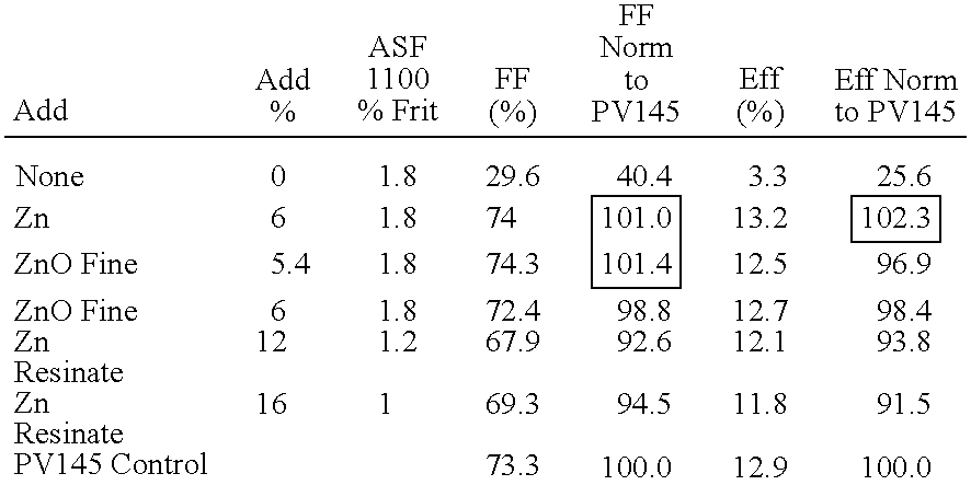
| Paste |
 |
Percents of glass frit and additive given in Table 4 are given in percent total thick film composition.
Experiments conducted and detailed in Table 4 illustrate the use of various types of Zn-containing additives and their effect on the thick film composition. Thick film silver paste compositions containing other forms and particle sizes of Zn and ZnO also achieve excellent electrical contact to Si solar cells. The Zn resinate used was 22% Zinc Hex-Cem obtained from OMG, Cleveland, Ohio.
| TABLE 5 |
| Effect of Mixed Oxide Additions on Thick Film Silver |
| Paste |
 |
Percents of glass frit and additive given in Table 5 are given in percent total thick film composition.
Thick film silver paste compositions comprising a mixture of oxide frits also demonstrate much improved performance.
| TABLE 6 |
| Effect of Other Oxide Additions on Thick Film Silver |
| Paste |
 |
| *ASF1100 glass frit is commercially available from Asahi Glass Company |
Percents of glass frit and additive given in Table 6 are given in percent total thick film composition.
All oxide additions, detailed in Table 6 above, to thick film silver paste result in solar cell performance improvement.
| TABLE 7 |
| Effect of ZnO Additive Level on Thick |
| Film Silver Paste Adhesion to Si |
| % ASF1100 Frit | % ZnO | Adh (g) | Normalized Adh (%) |
| 1.2 | 4 | 558 | 186 |
| 2.4 | 4 | 466 | 155 |
| 1.8 | 6 | 441 | 147 |
| 1.2 | 8 | 332 | 111 |
| 2.4 | 8 | 282 | 94 |
| *ASF1100 glass frit is commercially available from Asahi Glass Company | |||
Percents of glass frit and additive given in Table 7 are given in percent total thick film composition.
Claims (6)
1. A thick film conductive composition comprising:
a) electrically conductive silver powder;
b) zinc-containing additive, wherein the zinc-containing additive is ZnO and wherein the particle size of said ZnO is within the range of 7 nanometers to 60 nanometers;
c) one or more glass frits wherein said glass frits are lead-free; dispersed in
d) organic medium.
2. A thick film conductive composition comprising:
a) electrically conductive silver powder;
b) zinc-containing additive, wherein the zinc containing additive is ZnO, and wherein said ZnO is present in an amount of 7 to 16 wt % of the total composition;
c) one or more glass frits wherein said glass frits are lead-free; dispersed in
d) organic medium.
3. The glass frit of claim 1 or 2 comprising, based on weight percent total glass composition:
SiO2 0.1-8
Al2O3 0-4
B2O3 8-25
CaO 0-1
ZnO 0-42
Na2O 0-4
Li2O 0-3.5
Bi2O3 28-85
Ag2O 0-3 CeO2 0-4.5
SnO2 0-3.5, and
BiF3 0-15.
4. The composition of claim 1 or 2 further comprising an additional metal/metal oxide additive selected from (a) a metal wherein said metal is selected from Zn, Gd, Ce, Zr, Ti, Mn, Sn, Ru, Co, Fe, Cu, and Cr; (b) a metal oxide of one or more of the metals selected from Gd, Ce, Zr, Ti, Mn, Sn, Ru, Co, Fe, Cu and Cr; (c) any compounds that can generate the metal oxides of (b) upon firing; and (d) mixtures thereof.
5. The composition of claim 1 or 2 , wherein the glass frit comprises: Bi2O3, B2O3 8-25 weight percent and further comprises one or more components selected from the group consisting of: SiO2, P2O5, GeO2, and V2O5.
6. The thick film conductive composition of claim 2 , wherein the particle size of said zinc-containing additive is in the range of 7 nanometers to less than 100 nanometers.
Priority Applications (11)
| Application Number | Priority Date | Filing Date | Title |
|---|---|---|---|
| US11/106,259 US7435361B2 (en) | 2005-04-14 | 2005-04-14 | Conductive compositions and processes for use in the manufacture of semiconductor devices |
| AU2006201558A AU2006201558A1 (en) | 2005-04-14 | 2006-04-12 | Conductive compositions and processes for use in the manufacture of semiconductor devices |
| EP10011534A EP2306468B1 (en) | 2005-04-14 | 2006-04-13 | Conductive compositions and processes for their use in the manufacture of semiconductor devices |
| EP06252074A EP1713092B1 (en) | 2005-04-14 | 2006-04-13 | Conductive compositions and processes for their use in the manufacture of semiconductor devices |
| TW095113536A TWI348710B (en) | 2005-04-14 | 2006-04-14 | Conductive compositions and processes for use in the manufacture of semiconductor devices |
| KR1020060033938A KR100837994B1 (en) | 2005-04-14 | 2006-04-14 | Conductive compositions and processes for use in the manufacture of semiconductor devices |
| JP2006112244A JP5395995B2 (en) | 2005-04-14 | 2006-04-14 | Conductive compositions and methods used in the manufacture of semiconductor devices |
| CN2006100748056A CN101055896B (en) | 2005-04-14 | 2006-04-14 | Conductive compositions and substrate, electrode and semiconductor device,and processes for the manufacture of semiconductor devices |
| US12/176,697 US7935277B2 (en) | 2005-04-14 | 2008-07-21 | Conductive compositions and processes for use in the manufacture of semiconductor devices |
| US13/098,855 US8383017B2 (en) | 2005-04-14 | 2011-05-02 | Conductive compositions and processes for use in the manufacture of semiconductor devices |
| US13/776,213 US20130234271A1 (en) | 2005-04-14 | 2013-02-25 | Conductive compositions and processes for use in the manufacture of semiconductor devices |
Applications Claiming Priority (1)
| Application Number | Priority Date | Filing Date | Title |
|---|---|---|---|
| US11/106,259 US7435361B2 (en) | 2005-04-14 | 2005-04-14 | Conductive compositions and processes for use in the manufacture of semiconductor devices |
Related Child Applications (1)
| Application Number | Title | Priority Date | Filing Date |
|---|---|---|---|
| US12/176,697 Division US7935277B2 (en) | 2005-04-14 | 2008-07-21 | Conductive compositions and processes for use in the manufacture of semiconductor devices |
Publications (2)
| Publication Number | Publication Date |
|---|---|
| US20060231801A1 US20060231801A1 (en) | 2006-10-19 |
| US7435361B2 true US7435361B2 (en) | 2008-10-14 |
Family
ID=36688074
Family Applications (4)
| Application Number | Title | Priority Date | Filing Date |
|---|---|---|---|
| US11/106,259 Expired - Fee Related US7435361B2 (en) | 2005-04-14 | 2005-04-14 | Conductive compositions and processes for use in the manufacture of semiconductor devices |
| US12/176,697 Expired - Fee Related US7935277B2 (en) | 2005-04-14 | 2008-07-21 | Conductive compositions and processes for use in the manufacture of semiconductor devices |
| US13/098,855 Expired - Fee Related US8383017B2 (en) | 2005-04-14 | 2011-05-02 | Conductive compositions and processes for use in the manufacture of semiconductor devices |
| US13/776,213 Abandoned US20130234271A1 (en) | 2005-04-14 | 2013-02-25 | Conductive compositions and processes for use in the manufacture of semiconductor devices |
Family Applications After (3)
| Application Number | Title | Priority Date | Filing Date |
|---|---|---|---|
| US12/176,697 Expired - Fee Related US7935277B2 (en) | 2005-04-14 | 2008-07-21 | Conductive compositions and processes for use in the manufacture of semiconductor devices |
| US13/098,855 Expired - Fee Related US8383017B2 (en) | 2005-04-14 | 2011-05-02 | Conductive compositions and processes for use in the manufacture of semiconductor devices |
| US13/776,213 Abandoned US20130234271A1 (en) | 2005-04-14 | 2013-02-25 | Conductive compositions and processes for use in the manufacture of semiconductor devices |
Country Status (7)
| Country | Link |
|---|---|
| US (4) | US7435361B2 (en) |
| EP (2) | EP2306468B1 (en) |
| JP (1) | JP5395995B2 (en) |
| KR (1) | KR100837994B1 (en) |
| CN (1) | CN101055896B (en) |
| AU (1) | AU2006201558A1 (en) |
| TW (1) | TWI348710B (en) |
Cited By (28)
| Publication number | Priority date | Publication date | Assignee | Title |
|---|---|---|---|---|
| RU2174876C1 (en) * | 2000-09-25 | 2001-10-20 | Галда Александр Васильевич | Sprinkler unit nozzle head |
| US20080223446A1 (en) * | 2005-04-14 | 2008-09-18 | E.I. Du Pont De Nemours And Company | Method of manufacture of semiconductor device and conductive compositions used therein |
| US20090044858A1 (en) * | 2005-04-14 | 2009-02-19 | Wang Yueli Y | Method of Manufacture of Semiconductor Device and Conductive Compositions Used Therein |
| US20090101190A1 (en) * | 2006-03-20 | 2009-04-23 | Ferro Corporation | Solar Cell Contacts Containing Aluminum And At Least One Of Boron, Titanium, Nickel, Tin, Silver, Gallium, Zinc, Indium And Copper |
| US20090120483A1 (en) * | 2005-04-14 | 2009-05-14 | E. I. Du Pont De Nemours And Company | Conductive compositions and processes for use in the manufacture of semiconductor devices |
| US20090229665A1 (en) * | 2008-03-13 | 2009-09-17 | E. I. Du Pont De Nemours And Company | Aluminum pastes and use thereof in the production of silicon solar cells |
| US20090255584A1 (en) * | 2008-04-09 | 2009-10-15 | E.I. Du Pont De Nemours And Company | Conductive compositions and processes for use in the manufacture of semiconductor devices |
| US20100154883A1 (en) * | 2006-09-25 | 2010-06-24 | Ecn Energieonderzoek Centrum Nederland | Method of manufacturing crystalline silicon solar cells with improved surface passivation |
| US20100175754A1 (en) * | 2005-12-21 | 2010-07-15 | E.I. Du Pont De Nemours And Company | Paste for solar cell electrodes, method for the manufacture of solar cell electrodes, and the solar cell |
| US20100258166A1 (en) * | 2009-04-09 | 2010-10-14 | E.I. Du Pont De Nemours And Company | Glass compositions used in conductors for photovoltaic cells |
| US20100258182A1 (en) * | 2009-04-08 | 2010-10-14 | E. I. Du Pont De Nemours And Company | Solar cell electrode |
| US20100267194A1 (en) * | 2006-08-29 | 2010-10-21 | Fraunhofer-Gesellschaft zur Förderung der angewandten Forschung e.V. | Method for applying electrical contacts on semiconducting substrates, semiconducting substrate and use of the method |
| US20100319771A1 (en) * | 2007-11-13 | 2010-12-23 | Stichting Energieonderzoek Centrum Nederland | Method of manufacturing crystalline silicon solar cells using co diffusion of boron and phosphorus |
| US20110057314A1 (en) * | 2009-09-08 | 2011-03-10 | E. I. Du Pont De Nemours And Company | Conductors for photovoltaic cells |
| WO2011035015A1 (en) | 2009-09-17 | 2011-03-24 | E. I. Du Pont De Nemours And Company | Thick-film conductive compositions with nano-sized zinc additive |
| US20110126897A1 (en) * | 2009-05-20 | 2011-06-02 | E. I. Du Pont De Nemours And Company | Composition for extruding fibers |
| US20110146776A1 (en) * | 2009-12-18 | 2011-06-23 | E.I. Du Pont De Nemours And Company | Glass compositions used in conductors for photovoltaic cells |
| US20110278507A1 (en) * | 2010-05-11 | 2011-11-17 | E. I. Du Pont De Nemours And Company | Thick film silver pastes containing iodonium and/or sulfonium salts and their use in photovoltaic cells |
| US20120138142A1 (en) * | 2005-06-03 | 2012-06-07 | Ferro Corporation | Lead free solar cell contacts |
| WO2013023181A1 (en) | 2011-08-11 | 2013-02-14 | E. I. Du Pont De Nemours And Company | Silver paste with no or poor fire-through capability and use thereof for a solar cell metallisation |
| US8568619B2 (en) | 2009-06-17 | 2013-10-29 | Asahi Glass Company, Limited | Glass frit for forming electrode, and electrically conductive paste for forming electrode and solar cell, utilizing same |
| US8741167B1 (en) * | 2010-06-16 | 2014-06-03 | E I Du Pont De Nemours And Company | Etching composition and its use in a method of making a photovoltaic cell |
| US8759668B2 (en) | 2006-03-20 | 2014-06-24 | Heraeus Precious Metals North America Conshohocken Llc | Aluminum-boron solar cell contacts |
| US20140370261A1 (en) * | 2011-12-06 | 2014-12-18 | Dbfz Deutsches Biomasseforschungszentrum Gemeinnuetzige Gmbh | Electronically conductive enamel composition |
| US8999431B2 (en) | 2008-12-01 | 2015-04-07 | University Of Massachusetts Lowell | Conductive formulations for use in electrical, electronic and RF applications |
| US9038483B2 (en) | 2009-09-08 | 2015-05-26 | University Of Massachusetts | Wireless passive radio-frequency strain and displacement sensors |
| US9362017B2 (en) | 2010-10-28 | 2016-06-07 | Lg Innotek Co., Ltd. | Paste composition for front electrode of solar cell, and solar cell including the same |
| US20160204303A1 (en) * | 2013-08-21 | 2016-07-14 | Gtat Corporation | Using an active solder to couple a metallic article to a photovoltaic cell |
Families Citing this family (141)
| Publication number | Priority date | Publication date | Assignee | Title |
|---|---|---|---|---|
| JP2004162096A (en) * | 2002-11-11 | 2004-06-10 | Sumitomo Electric Ind Ltd | Electroless plating paste, and method for producing metal structure and fine metal component using the same |
| US9159568B2 (en) * | 2006-02-04 | 2015-10-13 | Cypress Semiconductor Corporation | Method for fabricating memory cells having split charge storage nodes |
| JP2008010527A (en) * | 2006-06-28 | 2008-01-17 | Sharp Corp | Conductive paste for solar cell electrode |
| TWI399759B (en) | 2006-06-30 | 2013-06-21 | Mitsubishi Materials Corp | Electrode composition for forming solar cell, method for forming the same, and solar cell using electrode obtained by the forming method |
| JP5309521B2 (en) * | 2006-10-11 | 2013-10-09 | 三菱マテリアル株式会社 | Electrode forming composition, method for producing the same, and electrode forming method using the composition |
| JP5203970B2 (en) * | 2006-12-25 | 2013-06-05 | ナミックス株式会社 | Conductive paste for electrode formation on crystalline silicon substrate |
| WO2008078374A1 (en) * | 2006-12-25 | 2008-07-03 | Namics Corporation | Conductive paste for solar cell |
| US7731868B2 (en) * | 2007-04-12 | 2010-06-08 | E.I. Du Pont De Nemours And Company | Thick film conductive composition and process for use in the manufacture of semiconductor device |
| JP5169389B2 (en) * | 2007-04-19 | 2013-03-27 | 三菱マテリアル株式会社 | Method for manufacturing conductive reflective film |
| KR101280489B1 (en) * | 2007-05-09 | 2013-07-01 | 주식회사 동진쎄미켐 | A paste for producing electrode of solar cell |
| KR20080100057A (en) * | 2007-05-11 | 2008-11-14 | 주성엔지니어링(주) | Method for manufacturing crystalline silicon solar cell, apparatus and system for manufacturing same |
| TW200926210A (en) * | 2007-09-27 | 2009-06-16 | Murata Manufacturing Co | Ag electrode paste, solar battery cell, and process for producing the solar battery cell |
| CN101816048A (en) * | 2007-10-18 | 2010-08-25 | E.I.内穆尔杜邦公司 | Conductive compositions and processes for use in the manufacture of semiconductor devices: multiple busbars |
| WO2009052356A2 (en) * | 2007-10-18 | 2009-04-23 | E. I. Du Pont De Nemours And Company | Conductive compositions and processes for use in the manufacture of semiconductor devices |
| US7485245B1 (en) | 2007-10-18 | 2009-02-03 | E.I. Du Pont De Nemours And Company | Electrode paste for solar cell and solar cell electrode using the paste |
| KR20100080612A (en) | 2007-10-18 | 2010-07-09 | 이 아이 듀폰 디 네모아 앤드 캄파니 | Lead-free conductive compositions and processes for use in the manufacture of semiconductor devices: mg-containing additive |
| CN101816044A (en) * | 2007-10-18 | 2010-08-25 | E.I.内穆尔杜邦公司 | Conductive compositions and processes for use in the manufacture of semiconductor devices: Mg-containing additive |
| WO2009052343A1 (en) | 2007-10-18 | 2009-04-23 | E. I. Du Pont De Nemours And Company | Conductive compositions and processes for use in the manufacture of semiconductor devices: flux materials |
| US8226856B2 (en) | 2007-10-18 | 2012-07-24 | E I Du Pont De Nemours And Company | Lead-free conductive compositions and processes for use in the manufacture of semiconductor devices: flux materials |
| US20090107546A1 (en) * | 2007-10-29 | 2009-04-30 | Palo Alto Research Center Incorporated | Co-extruded compositions for high aspect ratio structures |
| KR101431266B1 (en) * | 2007-11-27 | 2014-08-20 | 엘지전자 주식회사 | Manufacturing method of solar cell |
| US8383011B2 (en) * | 2008-01-30 | 2013-02-26 | Basf Se | Conductive inks with metallo-organic modifiers |
| US7736546B2 (en) * | 2008-01-30 | 2010-06-15 | Basf Se | Glass frits |
| US8308993B2 (en) * | 2008-01-30 | 2012-11-13 | Basf Se | Conductive inks |
| JP5423045B2 (en) * | 2008-02-26 | 2014-02-19 | 三菱マテリアル株式会社 | Method for manufacturing solar cell and method for manufacturing solar cell module |
| US20090266409A1 (en) * | 2008-04-28 | 2009-10-29 | E.I.Du Pont De Nemours And Company | Conductive compositions and processes for use in the manufacture of semiconductor devices |
| WO2009146348A1 (en) * | 2008-05-28 | 2009-12-03 | E. I. Du Pont De Nemours And Company | Compositions containing submicron particles used in conductors for photovoltaic cells |
| US8008179B2 (en) * | 2008-05-28 | 2011-08-30 | E.I. Du Pont De Nemours And Company | Methods using silver compositions for micro-deposition direct writing silver conductor lines on photovoltaic wafers |
| EP2286417A1 (en) * | 2008-05-28 | 2011-02-23 | E. I. du Pont de Nemours and Company | Conductors for photovoltaic cells: compositions containing submicron particles |
| KR20110014674A (en) * | 2008-05-28 | 2011-02-11 | 이 아이 듀폰 디 네모아 앤드 캄파니 | Method of using a composition containing submicron particles used in photovoltaic conductors |
| US8158504B2 (en) | 2008-05-30 | 2012-04-17 | E. I. Du Pont De Nemours And Company | Conductive compositions and processes for use in the manufacture of semiconductor devices—organic medium components |
| EP2294586B1 (en) * | 2008-05-30 | 2013-07-17 | E. I. du Pont de Nemours and Company | Conductive compositions and processes for use in the manufacture of semiconductor devices |
| TW201007773A (en) * | 2008-06-06 | 2010-02-16 | Du Pont | Glass compositions used in conductors for photovoltaic cells |
| US8076777B2 (en) * | 2008-06-26 | 2011-12-13 | E. I. Du Pont De Nemours And Company | Glass compositions used in conductors for photovoltaic cells |
| DE102008032784A1 (en) * | 2008-07-02 | 2010-03-18 | Fraunhofer-Gesellschaft zur Förderung der angewandten Forschung e.V. | Pasty consistency composition for forming electrical contacts on a silicon solar wafer and contact made therewith |
| DE102008032554A1 (en) * | 2008-07-10 | 2010-01-14 | Fraunhofer-Gesellschaft zur Förderung der angewandten Forschung e.V. | Metal-containing composition, process for the production of electrical contact structures on electronic components and electronic component |
| KR20110044896A (en) * | 2008-08-13 | 2011-05-02 | 이 아이 듀폰 디 네모아 앤드 캄파니 | Multi-Element Metal Powders for Silicon Solar Cells |
| US20100037941A1 (en) * | 2008-08-13 | 2010-02-18 | E. I. Du Pont De Nemours And Company | Compositions and processes for forming photovoltaic devices |
| US8294024B2 (en) * | 2008-08-13 | 2012-10-23 | E I Du Pont De Nemours And Company | Processes for forming photovoltaic devices |
| JP5428669B2 (en) * | 2008-09-08 | 2014-02-26 | 三菱マテリアル株式会社 | Solar cell and manufacturing method thereof |
| US8609256B2 (en) * | 2008-10-02 | 2013-12-17 | E I Du Pont De Nemours And Company | Nickel-gold plateable thick film silver paste |
| TWI423462B (en) * | 2008-10-22 | 2014-01-11 | Ind Tech Res Inst | Method for manufacturing back electrode of twin crystal solar battery |
| US20140335651A1 (en) * | 2008-11-14 | 2014-11-13 | Sichuan Yinhe Chemical Co., Ltd. | Inks and pastes for solar cell fabrication |
| KR101048350B1 (en) * | 2008-12-17 | 2011-07-14 | 한양대학교 산학협력단 | Method for fabricating hybrid heterostructure composites of nanoparticles, solar cell using hybrid heterostructure composites of nanoparticles and fabrication method thereof |
| US8710355B2 (en) | 2008-12-22 | 2014-04-29 | E I Du Pont De Nemours And Company | Compositions and processes for forming photovoltaic devices |
| JP2010192858A (en) * | 2009-02-20 | 2010-09-02 | Mitsubishi Electric Corp | Solar cell and method of manufacturing the same |
| KR20110128208A (en) * | 2009-03-19 | 2011-11-28 | 이 아이 듀폰 디 네모아 앤드 캄파니 | Conductive Paste for Solar Cell Electrode |
| KR101269710B1 (en) * | 2009-03-27 | 2013-05-30 | 가부시키가이샤 히타치세이사쿠쇼 | Conductive paste and electronic part equipped with electrode wiring formed from same |
| KR20120007517A (en) * | 2009-03-30 | 2012-01-20 | 이 아이 듀폰 디 네모아 앤드 캄파니 | Uses in the manufacture of metal pastes and silicon solar cells |
| EP2417075A1 (en) * | 2009-04-09 | 2012-02-15 | E. I. du Pont de Nemours and Company | Glass compositions used in conductors for photovoltaic cells |
| WO2010118209A1 (en) * | 2009-04-09 | 2010-10-14 | E. I. Du Pont De Nemours And Company | Glass compositions used in conductors for photovoltaic cells |
| EP2432839A1 (en) * | 2009-05-20 | 2012-03-28 | E. I. Du Pont De Nemours And Company | Phase change ink composition |
| JP5242499B2 (en) * | 2009-05-25 | 2013-07-24 | シャープ株式会社 | SOLAR CELL MODULE, ITS MANUFACTURING METHOD, AND ELECTRONIC DEVICE MOUNTED WITH THE SOLAR CELL MODULE |
| US20100301479A1 (en) | 2009-05-28 | 2010-12-02 | E. I. Du Pont De Nemours And Company | Devices containing silver compositions deposited by micro-deposition direct writing silver conductor lines |
| TW201115592A (en) | 2009-06-19 | 2011-05-01 | Du Pont | Glass compositions used in conductors for photovoltaic cells |
| US8163587B2 (en) | 2009-07-02 | 2012-04-24 | Innovalight, Inc. | Methods of using a silicon nanoparticle fluid to control in situ a set of dopant diffusion profiles |
| US20110183504A1 (en) * | 2010-01-25 | 2011-07-28 | Innovalight, Inc. | Methods of forming a dual-doped emitter on a substrate with an inline diffusion apparatus |
| US20110003466A1 (en) * | 2009-07-02 | 2011-01-06 | Innovalight, Inc. | Methods of forming a multi-doped junction with porous silicon |
| US8420517B2 (en) * | 2009-07-02 | 2013-04-16 | Innovalight, Inc. | Methods of forming a multi-doped junction with silicon-containing particles |
| KR101144810B1 (en) | 2009-07-06 | 2012-05-11 | 엘지전자 주식회사 | Electrode paste for solar cell, solar cell using the paste, and manufacturing method of the solar cell |
| JP5649290B2 (en) | 2009-07-30 | 2015-01-07 | 株式会社ノリタケカンパニーリミテド | Lead-free conductive composition for solar cell electrode |
| KR101139459B1 (en) * | 2009-08-27 | 2012-04-30 | 엘지전자 주식회사 | Sollar Cell And Fabrication Method Thereof |
| ES2438745T3 (en) * | 2009-09-04 | 2014-01-20 | Basf Se | Composition for printing printed circuits as well as a procedure for the manufacture of solar cells |
| JP2013512571A (en) | 2009-11-25 | 2013-04-11 | イー・アイ・デュポン・ドウ・ヌムール・アンド・カンパニー | Method for forming silver back electrode of passivated emitter and back contact silicon solar cell |
| JP2013513974A (en) * | 2009-12-15 | 2013-04-22 | イー・アイ・デュポン・ドウ・ヌムール・アンド・カンパニー | Process for manufacturing MWT silicon solar cells |
| US20110143497A1 (en) * | 2009-12-16 | 2011-06-16 | E. I. Du Pont De Nemours And Company | Thick film conductive composition used in conductors for photovoltaic cells |
| WO2011074888A2 (en) * | 2009-12-17 | 2011-06-23 | 동우 화인켐 주식회사 | Electrode paste composition for rear surface of solar cell |
| KR20110069724A (en) * | 2009-12-17 | 2011-06-23 | 동우 화인켐 주식회사 | Silver paste composition for solar cell back electrode |
| US20110315210A1 (en) | 2009-12-18 | 2011-12-29 | E. I. Du Pont De Nemours And Company | Glass compositions used in conductors for photovoltaic cells |
| KR101045262B1 (en) * | 2009-12-21 | 2011-06-29 | 제일모직주식회사 | Adhesive composition for semiconductor for stealth dicing and adhesive film using same |
| JP5279699B2 (en) * | 2009-12-28 | 2013-09-04 | 株式会社ノリタケカンパニーリミテド | Conductive paste composition for solar cell |
| US20110195540A1 (en) | 2010-02-05 | 2011-08-11 | Hitachi Chemical Company, Ltd. | Composition for forming p-type diffusion layer, method for forming p-type diffusion layer, and method for producing photovoltaic cell |
| JP5362615B2 (en) * | 2010-02-22 | 2013-12-11 | Dowaエレクトロニクス株式会社 | Silver powder and method for producing the same |
| JP5540811B2 (en) * | 2010-03-24 | 2014-07-02 | 三菱マテリアル株式会社 | Conductive composition, method for producing solar cell using the same, and solar cell |
| JP5540810B2 (en) * | 2010-03-24 | 2014-07-02 | 三菱マテリアル株式会社 | Conductive composition, method for producing solar cell using the same, and solar cell |
| JP5416631B2 (en) | 2010-03-25 | 2014-02-12 | 株式会社日立製作所 | Glass composition and conductive paste for aluminum electrode wiring, electronic component including the aluminum electrode wiring, and method for manufacturing the electronic component |
| KR101569567B1 (en) | 2010-05-04 | 2015-11-16 | 이 아이 듀폰 디 네모아 앤드 캄파니 | Thick-film pastes containing lead-tellurium-boron-oxides, and their use in the manufacture of semiconductor devices |
| WO2012012167A1 (en) | 2010-06-30 | 2012-01-26 | Innovalight, Inc | Methods of forming a floating junction on a solar cell with a particle masking layer |
| KR101181190B1 (en) | 2010-07-30 | 2012-09-18 | 엘지이노텍 주식회사 | Solar cell and paste compisition for rear electrode of the same |
| JP5796281B2 (en) * | 2010-08-17 | 2015-10-21 | 日本電気硝子株式会社 | Electrode forming material |
| KR101210112B1 (en) | 2010-08-31 | 2012-12-07 | 엘지이노텍 주식회사 | Glass frit and paste compisition for front electrode of solar cell including the same, and solar sell |
| KR101374359B1 (en) * | 2010-09-15 | 2014-03-18 | 제일모직주식회사 | Paste for forming electrode of solar cell and solar cell using the same |
| US8562872B2 (en) | 2010-09-15 | 2013-10-22 | Cheil Industries, Inc. | Paste for solar cell electrode and solar cell prepared using the same |
| WO2012058358A1 (en) | 2010-10-28 | 2012-05-03 | Ferro Corporation | Solar cell metallizations containing metal additive |
| CN102456427A (en) * | 2010-10-30 | 2012-05-16 | 比亚迪股份有限公司 | Conductive paste and preparation method thereof |
| WO2012064323A1 (en) * | 2010-11-09 | 2012-05-18 | E. I. Du Pont De Nemours And Company | Thick-film paste compositions with phosphonium surfactant |
| CN103329280B (en) * | 2010-12-06 | 2017-02-08 | 信越化学工业株式会社 | Solar cell and solar-cell module |
| US8858843B2 (en) * | 2010-12-14 | 2014-10-14 | Innovalight, Inc. | High fidelity doping paste and methods thereof |
| CN102157219B (en) * | 2011-01-12 | 2012-06-27 | 西安银泰新能源材料科技有限公司 | Silver paste for positive electrode of crystalline silicon solar cell and preparation method thereof |
| WO2012099877A1 (en) * | 2011-01-18 | 2012-07-26 | Heraeus Precious Metals North America Conshohocken Llc | Electroconductive paste compositions and solar cell electrodes and contacts made therefrom |
| US20120234384A1 (en) * | 2011-03-15 | 2012-09-20 | E.I. Du Pont Nemours And Company | Conductive metal paste for a metal-wrap-through silicon solar cell |
| US20120234383A1 (en) * | 2011-03-15 | 2012-09-20 | E.I.Du Pont De Nemours And Company | Conductive metal paste for a metal-wrap-through silicon solar cell |
| DE102011016034A1 (en) | 2011-04-04 | 2012-10-04 | Fraunhofer-Gesellschaft zur Förderung der angewandten Forschung e.V. | Metal-containing composition, useful e.g. to produce contact structure, comprises electrically conductive metal powder and/or their alloy and/or organometallic compound of the conductive metal, first oxide material, and oxidizing agent |
| US8512463B2 (en) * | 2011-04-05 | 2013-08-20 | E I Du Pont De Nemours And Company | Thick film paste containing bismuth-tellurium-oxide and its use in the manufacture of semiconductor devices |
| US20120312369A1 (en) * | 2011-06-13 | 2012-12-13 | E I Du Pont De Nemours And Company | Thick film paste containing bismuth-based oxide and its use in the manufacture of semiconductor devices |
| US20120312368A1 (en) * | 2011-06-13 | 2012-12-13 | E I Du Pont De Nemours And Company | Thick film paste containing bismuth-based oxide and its use in the manufacture of semiconductor devices |
| JP5726698B2 (en) | 2011-07-04 | 2015-06-03 | 株式会社日立製作所 | Glass composition, glass frit containing the same, glass paste containing the same, and electric and electronic parts using the same |
| KR101259158B1 (en) * | 2011-08-23 | 2013-04-26 | 주식회사 휘닉스소재 | Crystallizable frit composition for forming electrode |
| TW201318995A (en) * | 2011-08-31 | 2013-05-16 | Nihon Yamamura Glass Co Ltd | Lead-free glass composition for conductor formation |
| KR101272998B1 (en) * | 2011-10-13 | 2013-06-10 | 엘지이노텍 주식회사 | Solar cell and solar cell module unsing the same |
| WO2013058418A1 (en) * | 2011-10-18 | 2013-04-25 | 동우 화인켐 주식회사 | Silver paste composition (2) for the back electrode of a solar cell |
| WO2013058417A1 (en) * | 2011-10-18 | 2013-04-25 | 동우 화인켐 주식회사 | Silver paste composition (1) for the back electrode of a solar cell |
| US9023254B2 (en) * | 2011-10-20 | 2015-05-05 | E I Du Pont De Nemours And Company | Thick film silver paste and its use in the manufacture of semiconductor devices |
| CN102403049B (en) * | 2011-11-22 | 2013-11-13 | 华东微电子技术研究所合肥圣达实业公司 | Leadless electrode silver paste for lightning protection ZnO piezoresistor and preparation method thereof |
| CN102426875B (en) * | 2011-12-31 | 2014-04-16 | 四川虹欧显示器件有限公司 | Conductive paste, preparation method thereof and electrode prepared from conductive paste |
| EP2805334A4 (en) * | 2012-01-16 | 2015-10-28 | Heraeus Precious Metals North America Conshohocken Llc | ALUMINUM SLIDE PASTE FOR BACK-SURFACE-PASSIVATED CELLS WITH LOCALLY OPENED CONTACT |
| CN104170020A (en) * | 2012-01-18 | 2014-11-26 | 赫劳斯贵金属北美康舍霍肯有限责任公司 | Metallization of Solar Cells Containing Organozinc Compounds |
| CN102543261A (en) * | 2012-02-29 | 2012-07-04 | 广州神州光电有限责任公司 | Electrode silver paste for ferrite magnetic core, preparation method and application thereof |
| CN102593232B (en) * | 2012-03-19 | 2014-09-03 | 厦门大学 | PN solar cell with transverse structure and manufacturing method for solar cell |
| ES2703905T3 (en) | 2012-04-17 | 2019-03-13 | Heraeus Precious Metals North America Conshohocken Llc | Paste for a thick, conductive film for solar cell contacts |
| KR20130117707A (en) * | 2012-04-17 | 2013-10-28 | 헤레우스 프레셔스 메탈즈 노스 아메리카 콘쇼호켄 엘엘씨 | Inorganic reaction system for electroconductive paste composition |
| CN103915128B (en) * | 2012-05-03 | 2016-06-08 | 苏州晶银新材料股份有限公司 | Photovoltaic cell back electrode electrocondution slurry |
| CN103855232B (en) * | 2012-12-07 | 2017-09-08 | 第一太阳能马来西亚有限公司 | Photovoltaic device and its manufacture method |
| US9776909B2 (en) * | 2013-02-01 | 2017-10-03 | Namics Corporation | Glass frit |
| US20140261662A1 (en) * | 2013-03-18 | 2014-09-18 | E I Du Pont De Nemours And Company | Method of manufacturing a solar cell electrode |
| CN104217782A (en) * | 2013-05-30 | 2014-12-17 | 苏州晶银新材料股份有限公司 | High-adhesion back electrode silver paste for photovoltaic cell |
| WO2015039023A1 (en) * | 2013-09-16 | 2015-03-19 | Heraeus Precious Metals North America Conshohocken Llc | Electroconductive paste with adhesion promoting glass |
| EP2848657A1 (en) * | 2013-09-16 | 2015-03-18 | Heraeus Precious Metals North America Conshohocken LLC | Electroconductive paste with adhesion promoting glass |
| KR101659131B1 (en) * | 2013-11-12 | 2016-09-22 | 제일모직주식회사 | Composition for forming solar cell electrode and electrode prepared using the same |
| US9240515B2 (en) | 2013-11-25 | 2016-01-19 | E I Du Pont De Nemours And Company | Method of manufacturing a solar cell |
| CN106104702B (en) * | 2014-03-20 | 2021-03-30 | 纳美仕有限公司 | Conductive paste, laminated ceramic component, printed wiring board, and electronic device |
| CN103943166B (en) * | 2014-04-18 | 2016-06-29 | 西安交通大学 | A kind of Ag (Pb, Sn)/rare earth crystal-silicon solar cell composite mortar and preparation method thereof |
| CN105174728A (en) * | 2014-06-10 | 2015-12-23 | 湖南利德电子浆料有限公司 | Glass powder for crystalline silicon solar cell front silver paste and preparation method thereof |
| CN106605270B (en) | 2014-08-28 | 2019-03-08 | E.I.内穆尔杜邦公司 | Copper-containing conductive paste and electrodes made therefrom |
| CN106575537A (en) | 2014-08-28 | 2017-04-19 | E.I.内穆尔杜邦公司 | Solar cells with copper electrodes |
| CN106663493A (en) | 2014-08-28 | 2017-05-10 | E.I.内穆尔杜邦公司 | Copper-containing conductive pastes and electrodes made therefrom |
| EP3076401A1 (en) | 2015-03-27 | 2016-10-05 | Heraeus Deutschland GmbH & Co. KG | Electro-conductive pastes comprising a metal compound |
| EP3275000A1 (en) | 2015-03-27 | 2018-01-31 | Heraeus Deutschland GmbH & Co. KG | Electro-conductive pastes comprising an oxide additive |
| JP2017041627A (en) | 2015-08-17 | 2017-02-23 | 信越化学工業株式会社 | Conductive paste, method for producing the same, and solar cell electrode using the same |
| KR101655378B1 (en) * | 2015-10-12 | 2016-09-07 | 주식회사 휘닉스소재 | Paste composition for forming solar cell front electrode, n-type solar cell front electrode formed by using the same composition, and solar cell including the same front electrode |
| JP6624930B2 (en) | 2015-12-26 | 2019-12-25 | 日亜化学工業株式会社 | Light emitting device and manufacturing method thereof |
| GB201600573D0 (en) * | 2016-01-12 | 2016-02-24 | Johnson Matthey Plc | Conductive paste, article and process |
| JP6683003B2 (en) | 2016-05-11 | 2020-04-15 | 日亜化学工業株式会社 | Semiconductor element, semiconductor device, and method for manufacturing semiconductor element |
| JP6720747B2 (en) | 2016-07-19 | 2020-07-08 | 日亜化学工業株式会社 | Semiconductor device, base and manufacturing method thereof |
| JP6714275B2 (en) * | 2016-08-23 | 2020-06-24 | ナミックス株式会社 | Conductive paste and solar cell |
| TWI745562B (en) | 2017-04-18 | 2021-11-11 | 美商太陽帕斯特有限責任公司 | Conductive paste composition and semiconductor devices made therewith |
| CN107721183B (en) * | 2017-08-28 | 2019-09-20 | 广州市儒兴科技开发有限公司 | Glass powder for double-sided PERC solar cell back electrode paste and preparation method thereof |
| CN108033684A (en) * | 2017-12-13 | 2018-05-15 | 海南中航特玻科技有限公司 | A kind of back of the body silver glass powder used for solar batteries and preparation method |
| JP6954130B2 (en) * | 2018-01-11 | 2021-10-27 | Agc株式会社 | Glass, glass powder, conductive paste and solar cells |
| CN113707359B (en) * | 2021-09-09 | 2023-04-28 | 南京汇聚新材料科技有限公司 | Electrode paste, conductive thick film and preparation method thereof |
| TWI839636B (en) * | 2021-09-09 | 2024-04-21 | 大陸商南京匯聚新材料科技有限公司 | Electrode paste and method of preparing conductive thick film therefrom |
Citations (15)
| Publication number | Priority date | Publication date | Assignee | Title |
|---|---|---|---|---|
| US4256513A (en) | 1978-10-19 | 1981-03-17 | Matsushita Electric Industrial Co., Ltd. | Photoelectric conversion device |
| US4737197A (en) | 1985-08-29 | 1988-04-12 | Sharp Kabushiki Kaisha | Solar cell with metal paste contact |
| US5645765A (en) * | 1996-05-09 | 1997-07-08 | Shoei Chemical Inc. | Lead-free conductive paste |
| JPH11330512A (en) | 1999-04-16 | 1999-11-30 | Sharp Corp | Solar cell electrodes |
| JP2001015782A (en) | 1999-06-29 | 2001-01-19 | Kyocera Corp | Solar cell element and method of manufacturing the same |
| JP2001127317A (en) | 1999-10-28 | 2001-05-11 | Kyocera Corp | Solar cell manufacturing method |
| JP2001313400A (en) | 2000-04-28 | 2001-11-09 | Kyocera Corp | Method of forming solar cell element |
| US20020005507A1 (en) | 1999-12-21 | 2002-01-17 | Murata Manufacturing Co., Ltd | Conductive paste and printed wiring board using the same |
| JP2003223813A (en) | 2002-01-30 | 2003-08-08 | Toyo Aluminium Kk | Paste composition and solar cell using the same |
| JP2004146521A (en) | 2002-10-23 | 2004-05-20 | Sharp Corp | Silver electrode paste and solar cell using the same |
| US20040104262A1 (en) * | 2001-04-09 | 2004-06-03 | Mears Sarah Jane | Use of conductor compositions in electronic circuits |
| US20040155227A1 (en) * | 2001-04-04 | 2004-08-12 | Artur Bechtloff | Conductive paste, article produced therewith with a conductive coating on glass, ceramic or enameled steel and method for the production thereof |
| US20040214016A1 (en) | 2003-04-28 | 2004-10-28 | Fumiya Adachi | Conductive paste and glass circuit structure |
| US20060001009A1 (en) * | 2004-06-30 | 2006-01-05 | Garreau-Iles Angelique Genevie | Thick-film conductive paste |
| US20060231801A1 (en) * | 2005-04-14 | 2006-10-19 | Carroll Alan F | Conductive compositions and processes for use in the manufacture of semiconductor devices |
Family Cites Families (19)
| Publication number | Priority date | Publication date | Assignee | Title |
|---|---|---|---|---|
| US4051074A (en) * | 1975-10-29 | 1977-09-27 | Shoei Kagaku Kogyo Kabushiki Kaisha | Resistor composition and method for its manufacture |
| US5378408A (en) * | 1993-07-29 | 1995-01-03 | E. I. Du Pont De Nemours And Company | Lead-free thick film paste composition |
| US5346651A (en) | 1993-08-31 | 1994-09-13 | Cerdec Corporation | Silver containing conductive coatings |
| EP0669656A3 (en) * | 1994-02-25 | 1996-02-28 | Matsushita Electric Industrial Co Ltd | Source / drain of MISFET in a semiconductor device and manufacturing method. |
| JP2000277778A (en) * | 1999-03-25 | 2000-10-06 | Kyocera Corp | Method of manufacturing solar cell element |
| US6787068B1 (en) * | 1999-10-08 | 2004-09-07 | E. I. Du Pont De Nemours And Company | Conductor composition |
| JP2001118425A (en) * | 1999-10-21 | 2001-04-27 | Murata Mfg Co Ltd | Conductive paste |
| JP3460657B2 (en) * | 2000-01-31 | 2003-10-27 | 株式会社村田製作所 | Photosensitive glass paste for multilayer wiring circuit board and method for manufacturing multilayer wiring circuit board |
| JP2001307547A (en) * | 2000-04-25 | 2001-11-02 | Murata Mfg Co Ltd | Conductive composition and printed circuit board using the same |
| JP3534684B2 (en) * | 2000-07-10 | 2004-06-07 | Tdk株式会社 | Conductive paste, external electrode and method of manufacturing the same |
| EP1451830B1 (en) * | 2001-09-20 | 2006-06-14 | E. I. du Pont de Nemours and Company | Silver conductor compositions for solar cell electrodes |
| US6787239B2 (en) * | 2001-11-30 | 2004-09-07 | Matsushita Electric Industrial Co., Ltd. | Electrode material, dielectric material and plasma display panel using them |
| JP2003197405A (en) | 2001-12-21 | 2003-07-11 | Tdk Corp | Resistor paste, resistor and electronic component |
| KR20050116431A (en) | 2004-06-07 | 2005-12-12 | 삼성에스디아이 주식회사 | A photosensitive paste composition, a pdp electrode prepared therefrom, and a pdp comprising the same |
| TW200612443A (en) | 2004-09-01 | 2006-04-16 | Tdk Corp | Thick-film resistor paste and thick-film resistor |
| US7384577B2 (en) * | 2005-03-09 | 2008-06-10 | E.I. Du Pont De Nemours And Company | Black conductive thick film compositions, black electrodes, and methods of forming thereof |
| JP4815828B2 (en) | 2005-03-11 | 2011-11-16 | Tdk株式会社 | Conductive paste, electronic component, and electronic device |
| US7462304B2 (en) | 2005-04-14 | 2008-12-09 | E.I. Du Pont De Nemours And Company | Conductive compositions used in the manufacture of semiconductor device |
| US7556748B2 (en) * | 2005-04-14 | 2009-07-07 | E. I. Du Pont De Nemours And Company | Method of manufacture of semiconductor device and conductive compositions used therein |
-
2005
- 2005-04-14 US US11/106,259 patent/US7435361B2/en not_active Expired - Fee Related
-
2006
- 2006-04-12 AU AU2006201558A patent/AU2006201558A1/en not_active Abandoned
- 2006-04-13 EP EP10011534A patent/EP2306468B1/en not_active Not-in-force
- 2006-04-13 EP EP06252074A patent/EP1713092B1/en not_active Revoked
- 2006-04-14 KR KR1020060033938A patent/KR100837994B1/en not_active Expired - Fee Related
- 2006-04-14 JP JP2006112244A patent/JP5395995B2/en not_active Expired - Fee Related
- 2006-04-14 TW TW095113536A patent/TWI348710B/en not_active IP Right Cessation
- 2006-04-14 CN CN2006100748056A patent/CN101055896B/en not_active Expired - Fee Related
-
2008
- 2008-07-21 US US12/176,697 patent/US7935277B2/en not_active Expired - Fee Related
-
2011
- 2011-05-02 US US13/098,855 patent/US8383017B2/en not_active Expired - Fee Related
-
2013
- 2013-02-25 US US13/776,213 patent/US20130234271A1/en not_active Abandoned
Patent Citations (15)
| Publication number | Priority date | Publication date | Assignee | Title |
|---|---|---|---|---|
| US4256513A (en) | 1978-10-19 | 1981-03-17 | Matsushita Electric Industrial Co., Ltd. | Photoelectric conversion device |
| US4737197A (en) | 1985-08-29 | 1988-04-12 | Sharp Kabushiki Kaisha | Solar cell with metal paste contact |
| US5645765A (en) * | 1996-05-09 | 1997-07-08 | Shoei Chemical Inc. | Lead-free conductive paste |
| JPH11330512A (en) | 1999-04-16 | 1999-11-30 | Sharp Corp | Solar cell electrodes |
| JP2001015782A (en) | 1999-06-29 | 2001-01-19 | Kyocera Corp | Solar cell element and method of manufacturing the same |
| JP2001127317A (en) | 1999-10-28 | 2001-05-11 | Kyocera Corp | Solar cell manufacturing method |
| US20020005507A1 (en) | 1999-12-21 | 2002-01-17 | Murata Manufacturing Co., Ltd | Conductive paste and printed wiring board using the same |
| JP2001313400A (en) | 2000-04-28 | 2001-11-09 | Kyocera Corp | Method of forming solar cell element |
| US20040155227A1 (en) * | 2001-04-04 | 2004-08-12 | Artur Bechtloff | Conductive paste, article produced therewith with a conductive coating on glass, ceramic or enameled steel and method for the production thereof |
| US20040104262A1 (en) * | 2001-04-09 | 2004-06-03 | Mears Sarah Jane | Use of conductor compositions in electronic circuits |
| JP2003223813A (en) | 2002-01-30 | 2003-08-08 | Toyo Aluminium Kk | Paste composition and solar cell using the same |
| JP2004146521A (en) | 2002-10-23 | 2004-05-20 | Sharp Corp | Silver electrode paste and solar cell using the same |
| US20040214016A1 (en) | 2003-04-28 | 2004-10-28 | Fumiya Adachi | Conductive paste and glass circuit structure |
| US20060001009A1 (en) * | 2004-06-30 | 2006-01-05 | Garreau-Iles Angelique Genevie | Thick-film conductive paste |
| US20060231801A1 (en) * | 2005-04-14 | 2006-10-19 | Carroll Alan F | Conductive compositions and processes for use in the manufacture of semiconductor devices |
Cited By (44)
| Publication number | Priority date | Publication date | Assignee | Title |
|---|---|---|---|---|
| RU2174876C1 (en) * | 2000-09-25 | 2001-10-20 | Галда Александр Васильевич | Sprinkler unit nozzle head |
| US8383017B2 (en) * | 2005-04-14 | 2013-02-26 | E I Du Pont De Nemours And Company | Conductive compositions and processes for use in the manufacture of semiconductor devices |
| US20080223446A1 (en) * | 2005-04-14 | 2008-09-18 | E.I. Du Pont De Nemours And Company | Method of manufacture of semiconductor device and conductive compositions used therein |
| US20090044858A1 (en) * | 2005-04-14 | 2009-02-19 | Wang Yueli Y | Method of Manufacture of Semiconductor Device and Conductive Compositions Used Therein |
| US20110203659A1 (en) * | 2005-04-14 | 2011-08-25 | E. I. Du Pont De Nemours And Company | Conductive compositions and processes for use in the manufacture of semiconductor devices |
| US20090120483A1 (en) * | 2005-04-14 | 2009-05-14 | E. I. Du Pont De Nemours And Company | Conductive compositions and processes for use in the manufacture of semiconductor devices |
| US7935277B2 (en) * | 2005-04-14 | 2011-05-03 | E. I. Du Pont De Nemours And Company | Conductive compositions and processes for use in the manufacture of semiconductor devices |
| US7906045B2 (en) * | 2005-04-14 | 2011-03-15 | E. I. Du Pont De Nemours And Company | Method of manufacture of semiconductor device and conductive compositions used therein |
| US8394297B2 (en) | 2005-04-14 | 2013-03-12 | E I Du Pont De Nemours And Company | Method of manufacture of semiconductor device and conductive compositions used therein |
| US8313673B2 (en) * | 2005-04-14 | 2012-11-20 | E I Du Pont De Nemours And Company | Method of manufacture of semiconductor device and conductive compositions used therein |
| US9105768B2 (en) * | 2005-06-03 | 2015-08-11 | Heraeus Precious Metals North America Conshohocken Llc | Lead free solar cell contacts |
| US20120138142A1 (en) * | 2005-06-03 | 2012-06-07 | Ferro Corporation | Lead free solar cell contacts |
| US20100175754A1 (en) * | 2005-12-21 | 2010-07-15 | E.I. Du Pont De Nemours And Company | Paste for solar cell electrodes, method for the manufacture of solar cell electrodes, and the solar cell |
| US7851012B2 (en) * | 2005-12-21 | 2010-12-14 | E.I. Du Pont De Nemours And Company | Paste for solar cell electrodes, method for the manufacture of solar cell electrodes, and the solar cell |
| US8575474B2 (en) * | 2006-03-20 | 2013-11-05 | Heracus Precious Metals North America Conshohocken LLC | Solar cell contacts containing aluminum and at least one of boron, titanium, nickel, tin, silver, gallium, zinc, indium and copper |
| US8759668B2 (en) | 2006-03-20 | 2014-06-24 | Heraeus Precious Metals North America Conshohocken Llc | Aluminum-boron solar cell contacts |
| US20090101190A1 (en) * | 2006-03-20 | 2009-04-23 | Ferro Corporation | Solar Cell Contacts Containing Aluminum And At Least One Of Boron, Titanium, Nickel, Tin, Silver, Gallium, Zinc, Indium And Copper |
| US20100267194A1 (en) * | 2006-08-29 | 2010-10-21 | Fraunhofer-Gesellschaft zur Förderung der angewandten Forschung e.V. | Method for applying electrical contacts on semiconducting substrates, semiconducting substrate and use of the method |
| US8709853B2 (en) * | 2006-09-25 | 2014-04-29 | Ecn Energieonderzoek Centrum Nederland | Method of manufacturing crystalline silicon solar cells with improved surface passivation |
| US20100154883A1 (en) * | 2006-09-25 | 2010-06-24 | Ecn Energieonderzoek Centrum Nederland | Method of manufacturing crystalline silicon solar cells with improved surface passivation |
| US20100319771A1 (en) * | 2007-11-13 | 2010-12-23 | Stichting Energieonderzoek Centrum Nederland | Method of manufacturing crystalline silicon solar cells using co diffusion of boron and phosphorus |
| US8445312B2 (en) * | 2007-11-13 | 2013-05-21 | Stichting Energieonderzoek Centrum Nederland | Method of manufacturing crystalline silicon solar cells using co diffusion of Boron and Phosphorus |
| US20090229665A1 (en) * | 2008-03-13 | 2009-09-17 | E. I. Du Pont De Nemours And Company | Aluminum pastes and use thereof in the production of silicon solar cells |
| US20090255584A1 (en) * | 2008-04-09 | 2009-10-15 | E.I. Du Pont De Nemours And Company | Conductive compositions and processes for use in the manufacture of semiconductor devices |
| US8999431B2 (en) | 2008-12-01 | 2015-04-07 | University Of Massachusetts Lowell | Conductive formulations for use in electrical, electronic and RF applications |
| US8263858B2 (en) * | 2009-04-08 | 2012-09-11 | E I Du Pont De Nemours And Company | Solar cell electrode |
| US20100258182A1 (en) * | 2009-04-08 | 2010-10-14 | E. I. Du Pont De Nemours And Company | Solar cell electrode |
| US20100258166A1 (en) * | 2009-04-09 | 2010-10-14 | E.I. Du Pont De Nemours And Company | Glass compositions used in conductors for photovoltaic cells |
| US20110126897A1 (en) * | 2009-05-20 | 2011-06-02 | E. I. Du Pont De Nemours And Company | Composition for extruding fibers |
| US8568619B2 (en) | 2009-06-17 | 2013-10-29 | Asahi Glass Company, Limited | Glass frit for forming electrode, and electrically conductive paste for forming electrode and solar cell, utilizing same |
| US20110057314A1 (en) * | 2009-09-08 | 2011-03-10 | E. I. Du Pont De Nemours And Company | Conductors for photovoltaic cells |
| WO2011031726A1 (en) | 2009-09-08 | 2011-03-17 | E. I. Du Pont De Nemours And Company | Conductors for photovoltaic cells |
| US9038483B2 (en) | 2009-09-08 | 2015-05-26 | University Of Massachusetts | Wireless passive radio-frequency strain and displacement sensors |
| WO2011035015A1 (en) | 2009-09-17 | 2011-03-24 | E. I. Du Pont De Nemours And Company | Thick-film conductive compositions with nano-sized zinc additive |
| US9076571B2 (en) | 2009-09-17 | 2015-07-07 | E I Du Pont De Nemours And Company | Thick-film conductive compositions with nano-sized zinc additive |
| US8252204B2 (en) * | 2009-12-18 | 2012-08-28 | E I Du Pont De Nemours And Company | Glass compositions used in conductors for photovoltaic cells |
| US20110146776A1 (en) * | 2009-12-18 | 2011-06-23 | E.I. Du Pont De Nemours And Company | Glass compositions used in conductors for photovoltaic cells |
| US20110278507A1 (en) * | 2010-05-11 | 2011-11-17 | E. I. Du Pont De Nemours And Company | Thick film silver pastes containing iodonium and/or sulfonium salts and their use in photovoltaic cells |
| US8741167B1 (en) * | 2010-06-16 | 2014-06-03 | E I Du Pont De Nemours And Company | Etching composition and its use in a method of making a photovoltaic cell |
| US9362017B2 (en) | 2010-10-28 | 2016-06-07 | Lg Innotek Co., Ltd. | Paste composition for front electrode of solar cell, and solar cell including the same |
| WO2013023181A1 (en) | 2011-08-11 | 2013-02-14 | E. I. Du Pont De Nemours And Company | Silver paste with no or poor fire-through capability and use thereof for a solar cell metallisation |
| US20140370261A1 (en) * | 2011-12-06 | 2014-12-18 | Dbfz Deutsches Biomasseforschungszentrum Gemeinnuetzige Gmbh | Electronically conductive enamel composition |
| US9546282B2 (en) * | 2011-12-06 | 2017-01-17 | Dbfz Deutsches Biomasseforschungszentrum Gemeinnuetzige Gmbh | Electronically conductive enamel composition |
| US20160204303A1 (en) * | 2013-08-21 | 2016-07-14 | Gtat Corporation | Using an active solder to couple a metallic article to a photovoltaic cell |
Also Published As
| Publication number | Publication date |
|---|---|
| EP1713092A2 (en) | 2006-10-18 |
| KR100837994B1 (en) | 2008-06-13 |
| JP2006332032A (en) | 2006-12-07 |
| US20110203659A1 (en) | 2011-08-25 |
| EP1713092B1 (en) | 2011-09-21 |
| CN101055896B (en) | 2011-11-30 |
| US20130234271A1 (en) | 2013-09-12 |
| AU2006201558A1 (en) | 2006-11-02 |
| US20090120483A1 (en) | 2009-05-14 |
| EP2306468B1 (en) | 2012-12-05 |
| TW200731292A (en) | 2007-08-16 |
| US8383017B2 (en) | 2013-02-26 |
| KR20060108545A (en) | 2006-10-18 |
| JP5395995B2 (en) | 2014-01-22 |
| US20060231801A1 (en) | 2006-10-19 |
| EP1713092A3 (en) | 2007-03-07 |
| US7935277B2 (en) | 2011-05-03 |
| EP2306468A1 (en) | 2011-04-06 |
| TWI348710B (en) | 2011-09-11 |
| CN101055896A (en) | 2007-10-17 |
Similar Documents
| Publication | Publication Date | Title |
|---|---|---|
| US7435361B2 (en) | Conductive compositions and processes for use in the manufacture of semiconductor devices | |
| US7731868B2 (en) | Thick film conductive composition and process for use in the manufacture of semiconductor device | |
| US8394297B2 (en) | Method of manufacture of semiconductor device and conductive compositions used therein | |
| EP1713095B1 (en) | Method of manufacture of semiconductor device and conductive compositions used therein | |
| US7780878B2 (en) | Lead-free conductive compositions and processes for use in the manufacture of semiconductor devices: Mg-containing additive | |
| US7790065B2 (en) | Conductive compositions and processes for use in the manufacture of semiconductor devices: Mg-containing additive | |
| US20090101210A1 (en) | Conductive compositions and processes for use in the manufacture of semiconductor devices: multiple busbars | |
| EP2203921A1 (en) | Lead-free conductive compositions and processes for use in the manufacture of semiconductor devices: flux materials | |
| WO2009052343A1 (en) | Conductive compositions and processes for use in the manufacture of semiconductor devices: flux materials | |
| US20090104456A1 (en) | Conductive compositions and processes for use in the manufacture of semiconductor devices | |
| WO2009052356A2 (en) | Conductive compositions and processes for use in the manufacture of semiconductor devices |
Legal Events
| Date | Code | Title | Description |
|---|---|---|---|
| AS | Assignment |
Owner name: E. I. DU PONT DE NEMOURS AND COMPANY, DELAWARE Free format text: ASSIGNMENT OF ASSIGNORS INTEREST;ASSIGNORS:CARROLL, ALAN FREDERICK;HANG, KENNETH WARREN;REEL/FRAME:016099/0671;SIGNING DATES FROM 20050519 TO 20050520 |
|
| FPAY | Fee payment |
Year of fee payment: 4 |
|
| REMI | Maintenance fee reminder mailed | ||
| LAPS | Lapse for failure to pay maintenance fees | ||
| STCH | Information on status: patent discontinuation |
Free format text: PATENT EXPIRED DUE TO NONPAYMENT OF MAINTENANCE FEES UNDER 37 CFR 1.362 |
|
| STCH | Information on status: patent discontinuation |
Free format text: PATENT EXPIRED DUE TO NONPAYMENT OF MAINTENANCE FEES UNDER 37 CFR 1.362 |
|
| FP | Lapsed due to failure to pay maintenance fee |
Effective date: 20161014 |