US7433308B2 - Method and system for multi-PHY addressing - Google Patents
Method and system for multi-PHY addressing Download PDFInfo
- Publication number
- US7433308B2 US7433308B2 US11/144,257 US14425705A US7433308B2 US 7433308 B2 US7433308 B2 US 7433308B2 US 14425705 A US14425705 A US 14425705A US 7433308 B2 US7433308 B2 US 7433308B2
- Authority
- US
- United States
- Prior art keywords
- channels
- flow control
- signal
- phy
- layer device
- Prior art date
- Legal status (The legal status is an assumption and is not a legal conclusion. Google has not performed a legal analysis and makes no representation as to the accuracy of the status listed.)
- Expired - Fee Related, expires
Links
Images


Classifications
-
- H—ELECTRICITY
- H04—ELECTRIC COMMUNICATION TECHNIQUE
- H04L—TRANSMISSION OF DIGITAL INFORMATION, e.g. TELEGRAPHIC COMMUNICATION
- H04L12/00—Data switching networks
- H04L12/54—Store-and-forward switching systems
- H04L12/56—Packet switching systems
- H04L12/5601—Transfer mode dependent, e.g. ATM
-
- H—ELECTRICITY
- H04—ELECTRIC COMMUNICATION TECHNIQUE
- H04L—TRANSMISSION OF DIGITAL INFORMATION, e.g. TELEGRAPHIC COMMUNICATION
- H04L49/00—Packet switching elements
- H04L49/40—Constructional details, e.g. power supply, mechanical construction or backplane
- H04L49/405—Physical details, e.g. power supply, mechanical construction or backplane of ATM switches
Definitions
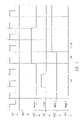
- FIG. 5 is a pin diagram illustrating the pins for packet interface signals of a PHY layer device for communication with a link layer device in the present invention.
- FIG. 2 is a flow diagram of the multi-PHY configuration 20 with a direct status indication.
- the PHY layer device 26 or 28 receives 30 a transmit clock signal 41 .
- the PHY layer device 26 or 28 determines 32 whether status indication represents a first group of four channels transmitted from the link layer device 22 . If status indication represents the first group of four channels, the PHY layer device 26 or 28 asserts 34 a Start signal 42 indicating that flow control signals received from the first group of four signals. However, if the flow control indication is not from the first group of four channels, the PHY layer device 26 or 28 de-asserts 36 the Start signal 42 .
- the PHY device 26 or 28 receives flow control indications of the Full[0:3] signals 49 - 52 for channels 4 through 7 .
- the PHY device 26 or 28 receives flow control indications Full[0:3] 49 - 52 from channels 8 through 11 .
- the PHY device 26 or 28 receives flow control indications on the Full[0:3] 49 - 52 from channels 17 through 15 .
- This round-robin sequence of operations repeats in a fifth clock cycle 47 e, as once again, the Start signal 48 is asserted indicating the commencement of the first group of four channels.
- RxChan [n:0] 64 PHY to link RxChan [n:0] signals are used to receive PHY channel.
- the RxChan signals are sampled when RxValid is asserted.
- the RxChan signals is set to zero when RxValid is de-asserted.
- the RxChan signals determine the channel associated with the RxData, RxSOCP, RxEOP, RxError, RxSize, and RxValid signals.
- RxData [p:0] 65 PHY to link Rx Data [p:0] signals are used to receive data.
- the Rx Data signals are sampled when RxValid is asserted.
- RxFull [s:0] 73 link to PHY RxFull [s:0] signals are use to receive flow control full indication from the link layer device to the PHY layer device. With cells, the RxFull [s:0] signals indicate that there is no room for more cells in the system. With packets, the RxFull [s:0] signals indicate that there is no room for more words in the system. The full status of the channels is time multiplexed onto the RxFull [s:0], which in one embodiment comprises four signals, as represented by RxFull [3:0]. Due to the source synchronous feature of the interface, the RxFull [s:0] signals are synchronous to the TxClk. RxClk 74 link to PHY RxClk signal is used to receive clock. This clock is used by the system device to sample all of the Rx signals. The PHY drives the Rx signals coincident to the rising edge of this clock.
Abstract
Multi-PHY addressing from source to destination in which n-number of channels or ports are used in a PHY layer device for communication with a link layer device. A single link layer to a single-PHY layer topology and a single link layer to a multi-PHY layer topology comprising multiple ports or channels receives a plurality of channels groups. Status indication signal is provided on continuous basis for the direct status for up to a predetermined number of channels.
Description
This application is a continuation of U.S. patent application Ser. No. 09/451,479, entitled “METHOD AND SYSTEM FOR MULTI-PHY ADDRESSING,” filed Nov. 30, 1999 now U.S. Pat. No. 6,030,979, and naming Jay Sethuram, Richard J. Weber, and Chandra S. Joshi as inventors.
The subject matter of this application is related to the subject matter of U.S. Application entitled “Source Synchronous Clocking”, Ser. No. 09/450,802, invented by Jay Sethuram, Richard Weber, and Chandra Shekh Joshi, and filed on Nov. 29, 1999, which is incorporated herein by reference.
1. Field of the Invention
The present invention relates generally to the field of telecommunication networks, and more particularly to ATM (Asynchronous Transfer Mode) interfaces between a link layer and a physical (PHY) layer.
2. Description of Related Art
Conventional communication interfaces between a link layer and a PHY layer use a polling technique for detecting incoming signal for each channel. Multiple ports and channels are coupled between the link layer and the PHY layer. Upon detecting incoming signal through one of the channels by a link layer device, the link layer device accesses the channel. Such technique establishes a master-slave type of relationship between the link layer device and the PHY layer device. Examples of conventional communication interfaces include prior Universal Test and Operation Physical Layer Protocol Interface for ATM (UTOPIA) Levels 1/2/3 interfaces.
Subsequent generations of communication interfaces may have a source synchronous clocking feature for operating at high frequencies. The polling technique used in a master-slave type of relationship is no longer applicable due to source synchronous clocking. In source synchronous clocking, a PHY layer device transmits data when data is ready to be transmitted.
Accordingly, it is desirable to have a method and system for providing multi-PHY addressing from source to destination at high speeds between the link layer device and the PHY layer device.
The invention provides a method and system for initiating transmission in a single-PHY or multi-PHY configuration from source to destination. In either configuration, a single electrical connection provides a point-to-point transfer between a PHY layer device and a link layer device. Each PHY layer device comprises one or more ports, and each port comprises one or more channels. Each of the multiple channels or ports is assigned to a different PHY address. Multi-PHY addresses are issued from source to destination. Multi-PHY addressing method from source to destination simplifies interface by eliminating polling.
A status indication signal provides continuous indication of the flow control status for each PHY. A status indication is provided in groups of four where the first group is identified by a START signal in which subsequent groups follow sequentially during transmission. In the transmit direction, a transmit flow control signal is generated in the receive clock domain while transmit data is sent in the transmit clock domain. In the receive direction, a receive flow control signal is generated in the transmit clock domain while receive data is sent in the receive clock domain.
In source synchronous interface, data transmission can be switched to any channel or port during a clock cycle. The present invention advantageously operates with source synchronous clocking for transfer of multi-PHY addressing from source to destination. The present invention further advantageously simplifies the flow control mechanism and reduces the number of signals required of for example, the UTOPIA Level 4 interface.
Preferably, the link layer device 17 or 22 operates at a transmission rate which maintains a maximal transmission rate generated from the PHY layer device 18, 26, or 28. If transmission rate of a link layer device 17 or 22 fails to keep up with the transmission rate of the PHY layer device 18, 26, or 28, the PHY layer devices 18, 26, or 28 automatically insert idle cells or packets in data stream. Similarly, on the receive end, the link layer device 17 or 22 is preferably designed to keep up with the receive data rate in preventing a FIFO overflow in the PHY layer device 18, 26, or 28.
In either single-PHY configuration 16 or multi-PHY configuration 20, the single electrical connection 19 or 29 transfers data at high speed, typically in excess of 10 Gbps. Data types can be of any kind, including multimedia data, network data, or Internet protocol traffic. In one embodiment of the multi-PHY configuration 20, the interface comprises six bits of address to support up to 64 channels or ports in the PHY layer device 24. During a clock cycle, the data transfer can be switched from one channel to another channel in the multi-PHY configuration 20.
Each of the PHY 26 or 28 device has one or more ports. The PHY device 26 provides a port 25 a, 25 b, 25 c, and 25 d while the PHY device 28 provides a port 27 a, a port 27 b, a port 27 c, and a port 27 d. Each of the ports 25 a-d and 27 a-d has one or more channels for data transmission. In one embodiment, the PHY device 26 have four channels where each channel is on separate ports 25 a, 25 b, 25 c, or 25 d. In an alternate embodiment, there are a set of four channels for each of the ports 25 a, 25 b, 25 c, and 25 d. A status indication for first set of four channels are multiplexed through the port 25 a, a status indication for second set of four channels are multiplexed through the port 25 b, a status indication for third set of four channels are multiplexed through the port 25 c, and a status indication for fourth set of four channels are multiplexed through the port 25 d.
Signals Full[0-3] 43-46 correspond to receive flow control signals from channels 0, 1, 2, and 3, respectively. In the transmit direction, each of the flow control signals Full[0-3] 43-46 are received from the PHY layer 17 to the link layer 18 coincident with a RxClk. In other words, the flow control signals Full[0-3] 43-46 are received in a receive clock domain while data is transmitted in a transmit clock domain. The flow control signals Full[0:3] 43-46 indicates to a sending or source device on whether a receiving or destination device is full or not. If a receiving or destination device if full, the sending or sourcing device stops data transfer; otherwise, the sending device continues data transfer. Similarly, in the receive direction each of the flow control signals Full[0-3] 43-46 are received from the link layer 18 to the PHY layer 17 coincident with TxClk 41. In other words, the flow control signals Full[0-3] 43-46 are received in a transmit clock domain while data is sent in a received clock domain. The flow control signals Full[0:3] 43-46 indicates to a sending or source device on whether a receiving or destination device is full or not. If a destination device if full, the sourcing device stops data transfer; otherwise, the sending device continues data transfer.
During a second clock cycle 47 b, the PHY device 26 or 28 receives flow control indications of the Full[0:3] signals 49-52 for channels 4 through 7. During a third clock cycle 47 c, the PHY device 26 or 28 receives flow control indications Full[0:3] 49-52 from channels 8 through 11. During a fourth clock cycle 47 d, the PHY device 26 or 28 receives flow control indications on the Full[0:3] 49-52 from channels 17 through 15. This round-robin sequence of operations repeats in a fifth clock cycle 47 e, as once again, the Start signal 48 is asserted indicating the commencement of the first group of four channels. Although sixteen channels are illustrated in this embodiment, one of ordinary skill in the art can extend or reduce the number of channels multiplexed and adjust the timing duration of the Start signal 48 without departing from the spirit of this invention. The number of channels may be increased to receive flow control signal without increasing the number of signals for n number of channels. Flow control status information is sent back to a sending device or a source device with every clock indicating whether or not a receiving device is full or not.
The transmit error TxError signal 58 indicates whether an error has been detected during transmit, such errors including bit errors and packet errors. If a link layer or a system detects the TxError signal 58, then the system analyzes further on the type of error which caused the triggering of the TxError signal or bit 58.
In this set of transmit signals, the transmit flow control signals of TxFull[s:0] 62 are sent in the receive clock domain from PHY to link, while transmit data TxData [p:0] 54 is sent in the transmit clock domain from link to PHY. Moreover, the transmit flow control signal of TxStart 61 is transmitted in the receive clock domain from PHY to link, while transmit data. TxData [p:0] 54, is sent in the transmit clock domain from link to PHY.
| TABLE 1 |
| Packet Interface Signals - Transmit |
| Signal | Direction | Function |
| TxChannel [n:0] 53 | Link to PHY | TxChannel [n:0] signals transmit PHY channel. |
| The TxChannel signals are sampled when | ||
| TxValid is asserted. The TxChannel signals is | ||
| set to zero when TxValid is de-asserted. The | ||
| TxChannel signals determine the channel | ||
| associated with the TxData, TxSOCP, TxEOP, | ||
| TxError, TxSize, and TxValid signals. | ||
| TxData [p:0] 54 | Link to PHY | TxData [p:0] signals are used to transmit data. |
| The TxData signals are sample when TxValid is | ||
| asserted. The TxData signals is set to zero when | ||
| TxValid is de-asserted. | ||
| TxPrty [q:0] 55 | Link to PHY | TxPrty [q:0] signals are used to transmit control |
| and data parity. The TxPrty signals comprise correct | ||
| parity. | ||
| |
Link to PHY | TxSOCP signal is used to transmit Start of cell |
| or packet. The TxSOCP is sampled when | ||
| TxValid is asserted. The TxSOCP signal is set | ||
| to zero when TxValid is de-asserted. | ||
| |
Link to PHY | TxEOP signal is used to transmit end of packet. |
| The TxEOP signal is sampled when TxValid is | ||
| asserted. The TxEOP signal is set to zero when | ||
| TxValid is de-asserted. | ||
| |
Link to PHY | TxError signal is used to transmit data error. |
| The TxError signal is sampled when TxEOP and | ||
| TxValid are both asserted. The TxError signal | ||
| is set to zero at other times. | ||
| TxSize [r:0] 59 | Link to PHY | TxSize [r:0] are used to transmit octet count. A |
| value of zero indicates that all octets are valid. | ||
| The TxSize signals are sampled when TxEOP | ||
| and TxValid are both asserted. The TxSize is | ||
| set to zero at other times. | ||
| |
Link to PHY | TxValid signal is used to transmit data valid. |
| When the TxValid is de-asserted, the following | ||
| signals is driven to zero: TxChannel, TxData, | ||
| TxSOCP, TxEOP, TxSize. | ||
| |
PHY to Link | TxStart signal is used to transmit flow control |
| Start from the PHY device to the link | ||
| Due to the source synchronous | ||
| interface, the TxStart signal is | ||
| synchronous to the TxClk. | ||
| TxFull [s:0] 62 | PHY to Link | TxFull [s:0] signals are used to transmit flow |
| control full indication from the PHY device to | ||
| the link layer device. With cells, a TxFull | ||
| signal indicates that there is no room for more | ||
| cells in the PHY. With packets, a TxFull signal | ||
| indicates that there is no room for more words in | ||
| the PHY. The full status of channels is time | ||
| multiplexed on to these four signals. Note that | ||
| due to the source synchronous feature of the | ||
| interface, the TxFull signal is synchronous with | ||
| the RxClk. | ||
| |
PHY to Link | TxClk signal is used to transmit clock. The |
| device will use the TxClk to sample all | ||
| signals. The link layer device will drive | ||
| Signals coincident with the rising | ||
| clock. | ||
Correspondingly, the set of receive signals 64-74 generated from the PHY device 26 to the link layer device 22 is described below in Table 2.
| TABLE 2 |
| Packet Interface Signals - Receive |
| Signal | Direction | Function |
| RxChan [n:0] 64 | PHY to link | RxChan [n:0] signals are used to receive PHY |
| channel. The RxChan signals are sampled when | ||
| RxValid is asserted. The RxChan signals is set | ||
| to zero when RxValid is de-asserted. The | ||
| RxChan signals determine the channel | ||
| associated with the RxData, RxSOCP, RxEOP, | ||
| RxError, RxSize, and RxValid signals. | ||
| RxData [p:0] 65 | PHY to link | Rx Data [p:0] signals are used to receive data. |
| The Rx Data signals are sampled when RxValid | ||
| is asserted. The Rx Data signals is set to zero | ||
| when RxValid is de-asserted. | ||
| RxPrty [q:0] 66 | PHY to link | RxPrty [q:0] signals are used to receive control |
| and data parity. The RxPrty comprises correct parity. | ||
| |
PHY to link | RxSOCP is used to receive Start of cell or |
| packet. The RxSOCP signal is only sampled | ||
| when RxValid is asserted. The RxSOCP is set to zero | ||
| when RxValid is de-asserted. | ||
| |
PHY to link | RxEOP signal is used to receive end of packet. |
| The RxEOP signal is sampled when RxValid is | ||
| asserted. The RxEOP is set to zero when | ||
| RxValid is de-asserted. | ||
| |
PHY to link | RxError signal is used to receive data error. The |
| RxError signal is sampled when both RxValid | ||
| and RxEOP are asserted. The RxError signal is | ||
| set to zero when RxValid is de-asserted. | ||
| RxSize [r:0] 70 | PHY to link | RxSize [r:0] signals are used to receive octet |
| count. A value of zero indicates that all eight | ||
| octets are valid. The RxSize [r:0] signals are | ||
| sampled when both RxValid and RxEOP are | ||
| asserted. The RxSize [r:0] signal is set to zero | ||
| at other times. | ||
| |
PHY to link | RxValid signal is used to receive data valid. |
| When the RxValid signal is de-asserted, the | ||
| following signals is set to zero: RxChan, | ||
| RxData, RxSOCP, RxEOP, RxError, and RxSize. | ||
| |
link to PHY | RxStart signal is used to receive flow control |
| frame Start signal from the link layer device to | ||
| the PHY device. The RxStart signal is sometime | ||
| referred to as RxFrame signal. Due to the | ||
| source synchronous feature of the interface, the | ||
| RxStart signals is synchronous to the TxClk. | ||
| RxFull [s:0] 73 | link to PHY | RxFull [s:0] signals are use to receive flow |
| control full indication from the link layer device | ||
| to the PHY layer device. With cells, the RxFull | ||
| [s:0] signals indicate that there is no room for | ||
| more cells in the system. With packets, the | ||
| RxFull [s:0] signals indicate that there is no | ||
| room for more words in the system. The full | ||
| status of the channels is time multiplexed onto | ||
| the RxFull [s:0], which in one embodiment | ||
| comprises four signals, as represented by RxFull | ||
| [3:0]. Due to the source synchronous feature of | ||
| the interface, the RxFull [s:0] signals are | ||
| synchronous to the TxClk. | ||
| RxClk 74 | link to PHY | RxClk signal is used to receive clock. This |
| clock is used by the system device to sample all | ||
| of the Rx signals. The PHY drives the Rx | ||
| signals coincident to the rising edge of this | ||
| clock. | ||
In this set of receive signals, the receive flow control signals of RxFull[s:0] 73 are sent in the transmit clock domain from link to PHY, while receive data RxData[p:0] 65 is sent in the receive clock domain from PHY to link. Moreover, the transmit flow control signal of RxStart signal 72 is sent in the transmit clock domain from link to PHY, while receive data RxData[p:0] 65 is sent in the receive clock domain from PHY to link.
The above embodiments are only illustrative of the principles of this invention and are not intended to limit the invention to the particular embodiments described. For example, one having ordinary skill in the art should recognize that the pins for the packet interface signals and the ATM interface signals may be multiplexed to conserve the total pin counts on a semiconductor chip. Furthermore, one of ordinary skill in the art should recognize that the invention may be practiced within the spirit of the invention by transmitting signals from various sources including a system or a device that is equivalent to a link layer device for communication with a PHY layer device. Accordingly, various modifications, adaptations, and combinations of various features of the described embodiments can be practiced without departing from the scope of the invention as set forth in the following claims.
Claims (15)
1. A method comprising:
outputting a clock signal;
outputting a flow control signal; and
outputting a start signal, wherein
a value of the start signal, during a given cycle of the clock signal, identifies one of a plurality of cycles of a flow control frame,
during a first cycle of the cycles of the flow control frame, a value of the flow control signal corresponds to a first one of a plurality of channels, and
the channels communicatively couple a physical layer device and a link layer device.
2. The method of claim 1 , further comprising:
outputting a second flow control signal, wherein
during the first cycle of the flow control frame, a value of the second flow control signal corresponds to a first one of a second plurality of channels, and
the second plurality of channels communicatively couple the physical layer device and the link layer device.
3. The method of claim 2 , wherein
data conveyed via each of the channels is output via a first physical port, and
data conveyed via each of the second plurality of channels is output via a second physical port.
4. The method of claim 1 , wherein
during the first cycle of the flow control frame, the value of the flow control signal identifies whether the first one of the channels is capable of receiving more data.
5. The method of claim 1 , wherein
the flow control signal, the clock signal, and the start signal are output from the physical layer device to the link layer device.
6. The method of claim 1 , wherein
the flow control signal, the clock signal, and the start signal are output from the link layer device to the physical layer device.
7. The method of claim 1 , further comprising:
outputting a data signal; and
outputting one or more channel signals, wherein
a value the one or more channel signals, during a given cycle of the clock signal, identifies one of the plurality of channels, and
the data signal conveys data in the identified one of the plurality of channels during the given cycle of the clock signal.
8. An apparatus comprising:
a transmit interface, wherein
the transmit interface is configured to output a flow control signal, a transmit clock signal, and a start signal, and
a value the start signal, during a given cycle of the clock signal, indicates one of a plurality of cycles of a flow control frame,
during a first cycle of the cycles of the flow control frame, a value of the flow control signal corresponds to a first one of a plurality of channels, and
the channels communicatively couple a physical layer device and a link layer device.
9. The apparatus of claim 8 , wherein
the transmit interface and the receive interface are included in the physical layer device.
10. The apparatus of claim 8 , wherein
the transmit interface and the receive interface are included in the link layer device.
11. The apparatus of claim 8 , wherein
the transmit interface is configured to output a second flow control signal,
during the first cycle of the flow control frame, a value of the second flow control signal corresponds to a first one of a second plurality of channels, and
the second plurality of channels communicatively couple the physical layer device and the link layer device.
12. The apparatus of claim 11 , further comprising:
a first physical port and a second physical port, wherein
data conveyed via each of the channels is output via the first physical port, and
data conveyed via each of the second plurality of channels is output via the second physical port.
13. The apparatus of claim 8 , wherein
during the first cycle of the flow control frame, the value of the flow control signal identifies whether the first one of the channels is capable of receiving more data.
14. The apparatus of claim 8 , wherein
the transmit interface is configured to output a data signal and one or more channel signals, wherein
a value the one or more channel signals, during a given cycle of the clock signal, identifies one of the plurality of channels, and
the data signal conveys data in the identified one of the plurality of channels, during the given cycle of the clock signal.
15. A system comprising:
means for outputting a clock signal;
means for outputting a flow control signal; and
means for outputting a start signal, wherein
a value of the start signal, during a given cycle of the clock signal, identifies one of a plurality of cycles of a flow control frame,
during a first cycle of the cycles of the flow control frame, a value of the flow control signal corresponds to a first one of a plurality of channels, and
the channels communicatively couple a physical layer device and a link layer device.
Priority Applications (1)
| Application Number | Priority Date | Filing Date | Title |
|---|---|---|---|
| US11/144,257 US7433308B2 (en) | 1999-11-30 | 2005-06-03 | Method and system for multi-PHY addressing |
Applications Claiming Priority (2)
| Application Number | Priority Date | Filing Date | Title |
|---|---|---|---|
| US09/451,479 US6930979B1 (en) | 1999-11-30 | 1999-11-30 | Method and system for multi-PHY addressing |
| US11/144,257 US7433308B2 (en) | 1999-11-30 | 2005-06-03 | Method and system for multi-PHY addressing |
Related Parent Applications (1)
| Application Number | Title | Priority Date | Filing Date |
|---|---|---|---|
| US09/451,479 Continuation US6930979B1 (en) | 1999-11-30 | 1999-11-30 | Method and system for multi-PHY addressing |
Publications (2)
| Publication Number | Publication Date |
|---|---|
| US20050226160A1 US20050226160A1 (en) | 2005-10-13 |
| US7433308B2 true US7433308B2 (en) | 2008-10-07 |
Family
ID=34825843
Family Applications (2)
| Application Number | Title | Priority Date | Filing Date |
|---|---|---|---|
| US09/451,479 Expired - Fee Related US6930979B1 (en) | 1999-11-30 | 1999-11-30 | Method and system for multi-PHY addressing |
| US11/144,257 Expired - Fee Related US7433308B2 (en) | 1999-11-30 | 2005-06-03 | Method and system for multi-PHY addressing |
Family Applications Before (1)
| Application Number | Title | Priority Date | Filing Date |
|---|---|---|---|
| US09/451,479 Expired - Fee Related US6930979B1 (en) | 1999-11-30 | 1999-11-30 | Method and system for multi-PHY addressing |
Country Status (1)
| Country | Link |
|---|---|
| US (2) | US6930979B1 (en) |
Families Citing this family (1)
| Publication number | Priority date | Publication date | Assignee | Title |
|---|---|---|---|---|
| US20070047579A1 (en) * | 2005-08-23 | 2007-03-01 | Suvhasis Mukhopadhyay | Multipacket interface |
Citations (6)
| Publication number | Priority date | Publication date | Assignee | Title |
|---|---|---|---|---|
| US5748018A (en) | 1996-01-30 | 1998-05-05 | Nec Corporation | Data transfer system for an integrated circuit, capable of shortening a data transfer cycle |
| US5854840A (en) | 1995-04-26 | 1998-12-29 | Scientific-Atlanta, Inc. | Data transmission protocol method and apparatus |
| US6195597B1 (en) | 1998-04-17 | 2001-02-27 | Sony Corporation | Onboard information processing apparatus and automobile |
| US6356557B1 (en) | 1998-10-14 | 2002-03-12 | Ahead Communications Systems, Inc. | Hot insertable UTOPIA interface with automatic protection switching for backplane applications |
| US6690670B1 (en) * | 1998-03-13 | 2004-02-10 | Paradyne Corporation | System and method for transmission between ATM layer devices and PHY layer devices over a serial bus |
| US6865188B1 (en) * | 1997-02-17 | 2005-03-08 | Communication & Control Electronics Limited | Local communication system |
Family Cites Families (6)
| Publication number | Priority date | Publication date | Assignee | Title |
|---|---|---|---|---|
| JPH07307738A (en) * | 1994-05-13 | 1995-11-21 | Mitsubishi Electric Corp | Protocol processor |
| US5784559A (en) * | 1995-11-06 | 1998-07-21 | Sun Microsystems, Inc. | Full duplex flow control for ethernet networks |
| US5784370A (en) * | 1995-12-29 | 1998-07-21 | Cypress Semiconductor Corp. | Method and apparatus for regenerating a control signal at an asynchronous transfer mode (ATM) layer or a physical (PHY) layer |
| US6185630B1 (en) * | 1997-02-14 | 2001-02-06 | Advanced Micro Devices, Inc. | Device initializing system with programmable array logic configured to cause non-volatile memory to output address and data information to the device in a prescribed sequence |
| US6141352A (en) * | 1997-10-10 | 2000-10-31 | Nortel Networks Limited | Method and apparatus for transmitting 10BASE-T signals across a 100BASE-X physical layer device service interface |
| US6345052B1 (en) * | 1998-11-05 | 2002-02-05 | Pmc-Sierra, Ltd. | Method and apparatus for the reliable transition of status signals from an interface device when using a localized sampling architecture |
-
1999
- 1999-11-30 US US09/451,479 patent/US6930979B1/en not_active Expired - Fee Related
-
2005
- 2005-06-03 US US11/144,257 patent/US7433308B2/en not_active Expired - Fee Related
Patent Citations (6)
| Publication number | Priority date | Publication date | Assignee | Title |
|---|---|---|---|---|
| US5854840A (en) | 1995-04-26 | 1998-12-29 | Scientific-Atlanta, Inc. | Data transmission protocol method and apparatus |
| US5748018A (en) | 1996-01-30 | 1998-05-05 | Nec Corporation | Data transfer system for an integrated circuit, capable of shortening a data transfer cycle |
| US6865188B1 (en) * | 1997-02-17 | 2005-03-08 | Communication & Control Electronics Limited | Local communication system |
| US6690670B1 (en) * | 1998-03-13 | 2004-02-10 | Paradyne Corporation | System and method for transmission between ATM layer devices and PHY layer devices over a serial bus |
| US6195597B1 (en) | 1998-04-17 | 2001-02-27 | Sony Corporation | Onboard information processing apparatus and automobile |
| US6356557B1 (en) | 1998-10-14 | 2002-03-12 | Ahead Communications Systems, Inc. | Hot insertable UTOPIA interface with automatic protection switching for backplane applications |
Non-Patent Citations (1)
| Title |
|---|
| Jay Sethuram, Richard J. Weber, Chandra S. Joshi; "Method And System For Source Synchronous Clocking;" filed Nov. 29, 1999; U.S. Appl. No. 09/450,802; including Specification: pp. 1-16; Drawings: Figures 1-5 on 5 sheets. |
Also Published As
| Publication number | Publication date |
|---|---|
| US6930979B1 (en) | 2005-08-16 |
| US20050226160A1 (en) | 2005-10-13 |
Similar Documents
| Publication | Publication Date | Title |
|---|---|---|
| US6385208B1 (en) | Serial media independent interface | |
| US6229822B1 (en) | Communications system for receiving and transmitting data cells | |
| EP1045557B1 (en) | ATM switching system | |
| JP3412825B2 (en) | Method and apparatus for switching data packets over a data network | |
| EP1454440B1 (en) | Method and apparatus for providing optimized high speed link utilization | |
| US6215789B1 (en) | Local area network for the transmission and control of audio, video, and computer data | |
| US5530842A (en) | Generic backplane system which is configurable to serve different network access methods simultaneously | |
| US7296093B1 (en) | Network processor interface system | |
| EP1435754A1 (en) | Converter/bridge and method of operation between Ethernet and ATM interfaces | |
| US6535513B1 (en) | Multimedia and multirate switching method and apparatus | |
| US20050138238A1 (en) | Flow control interface | |
| US6810424B2 (en) | Link layer device and method of translating packets between transport protocols | |
| US8451827B2 (en) | Time-slot interchange circuit | |
| US7376767B1 (en) | Distributed buffering system having programmable interconnecting logic and applications thereof | |
| EP1315397B1 (en) | High-speed sequenced multi-channel bus | |
| US7433308B2 (en) | Method and system for multi-PHY addressing | |
| US6826187B1 (en) | Interfacing between a physical layer and a bus | |
| US6654838B1 (en) | Methods for performing bit sensitive parallel bus peer addressing | |
| US6826178B1 (en) | Apparatus for performing bit sensitive parallel bus peer addressing | |
| US20050169298A1 (en) | Link layer device with non-linear polling of multiple physical layer device ports | |
| US7594026B1 (en) | Method and apparatus for multi-phy communication without an ATM bus master | |
| WO2002015489A2 (en) | Switches and routers, with parallel domains operating at a reduced speed | |
| WO2000074317A1 (en) | Multi-atm layer, multi-phy layer bus architecture | |
| Cidon et al. | TechLAN: an experimental high-speed ATM LAN | |
| KR19980061552A (en) | Board Control Method in ATM Switching System Using General Flow Control |
Legal Events
| Date | Code | Title | Description |
|---|---|---|---|
| STCF | Information on status: patent grant |
Free format text: PATENTED CASE |
|
| FPAY | Fee payment |
Year of fee payment: 4 |
|
| FPAY | Fee payment |
Year of fee payment: 8 |
|
| FEPP | Fee payment procedure |
Free format text: MAINTENANCE FEE REMINDER MAILED (ORIGINAL EVENT CODE: REM.); ENTITY STATUS OF PATENT OWNER: LARGE ENTITY |
|
| LAPS | Lapse for failure to pay maintenance fees |
Free format text: PATENT EXPIRED FOR FAILURE TO PAY MAINTENANCE FEES (ORIGINAL EVENT CODE: EXP.); ENTITY STATUS OF PATENT OWNER: LARGE ENTITY |
|
| STCH | Information on status: patent discontinuation |
Free format text: PATENT EXPIRED DUE TO NONPAYMENT OF MAINTENANCE FEES UNDER 37 CFR 1.362 |
|
| FP | Lapsed due to failure to pay maintenance fee |
Effective date: 20201007 |