US7420428B2 - Low noise phase locked loop with a high precision lock detector - Google Patents
Low noise phase locked loop with a high precision lock detector Download PDFInfo
- Publication number
- US7420428B2 US7420428B2 US11/485,664 US48566406A US7420428B2 US 7420428 B2 US7420428 B2 US 7420428B2 US 48566406 A US48566406 A US 48566406A US 7420428 B2 US7420428 B2 US 7420428B2
- Authority
- US
- United States
- Prior art keywords
- signal
- frequency
- vco
- pfd
- voltage
- Prior art date
- Legal status (The legal status is an assumption and is not a legal conclusion. Google has not performed a legal analysis and makes no representation as to the accuracy of the status listed.)
- Active, expires
Links
Images


Classifications
-
- H—ELECTRICITY
- H03—ELECTRONIC CIRCUITRY
- H03L—AUTOMATIC CONTROL, STARTING, SYNCHRONISATION OR STABILISATION OF GENERATORS OF ELECTRONIC OSCILLATIONS OR PULSES
- H03L7/00—Automatic control of frequency or phase; Synchronisation
- H03L7/06—Automatic control of frequency or phase; Synchronisation using a reference signal applied to a frequency- or phase-locked loop
- H03L7/08—Details of the phase-locked loop
- H03L7/085—Details of the phase-locked loop concerning mainly the frequency- or phase-detection arrangement including the filtering or amplification of its output signal
- H03L7/095—Details of the phase-locked loop concerning mainly the frequency- or phase-detection arrangement including the filtering or amplification of its output signal using a lock detector
-
- H—ELECTRICITY
- H03—ELECTRONIC CIRCUITRY
- H03L—AUTOMATIC CONTROL, STARTING, SYNCHRONISATION OR STABILISATION OF GENERATORS OF ELECTRONIC OSCILLATIONS OR PULSES
- H03L7/00—Automatic control of frequency or phase; Synchronisation
- H03L7/06—Automatic control of frequency or phase; Synchronisation using a reference signal applied to a frequency- or phase-locked loop
- H03L7/08—Details of the phase-locked loop
- H03L7/085—Details of the phase-locked loop concerning mainly the frequency- or phase-detection arrangement including the filtering or amplification of its output signal
- H03L7/087—Details of the phase-locked loop concerning mainly the frequency- or phase-detection arrangement including the filtering or amplification of its output signal using at least two phase detectors or a frequency and phase detector in the loop
-
- H—ELECTRICITY
- H03—ELECTRONIC CIRCUITRY
- H03L—AUTOMATIC CONTROL, STARTING, SYNCHRONISATION OR STABILISATION OF GENERATORS OF ELECTRONIC OSCILLATIONS OR PULSES
- H03L7/00—Automatic control of frequency or phase; Synchronisation
- H03L7/06—Automatic control of frequency or phase; Synchronisation using a reference signal applied to a frequency- or phase-locked loop
- H03L7/08—Details of the phase-locked loop
- H03L7/085—Details of the phase-locked loop concerning mainly the frequency- or phase-detection arrangement including the filtering or amplification of its output signal
- H03L7/089—Details of the phase-locked loop concerning mainly the frequency- or phase-detection arrangement including the filtering or amplification of its output signal the phase or frequency detector generating up-down pulses
- H03L7/0891—Details of the phase-locked loop concerning mainly the frequency- or phase-detection arrangement including the filtering or amplification of its output signal the phase or frequency detector generating up-down pulses the up-down pulses controlling source and sink current generators, e.g. a charge pump
-
- H—ELECTRICITY
- H03—ELECTRONIC CIRCUITRY
- H03L—AUTOMATIC CONTROL, STARTING, SYNCHRONISATION OR STABILISATION OF GENERATORS OF ELECTRONIC OSCILLATIONS OR PULSES
- H03L7/00—Automatic control of frequency or phase; Synchronisation
- H03L7/06—Automatic control of frequency or phase; Synchronisation using a reference signal applied to a frequency- or phase-locked loop
- H03L7/08—Details of the phase-locked loop
- H03L7/14—Details of the phase-locked loop for assuring constant frequency when supply or correction voltages fail
-
- H—ELECTRICITY
- H03—ELECTRONIC CIRCUITRY
- H03L—AUTOMATIC CONTROL, STARTING, SYNCHRONISATION OR STABILISATION OF GENERATORS OF ELECTRONIC OSCILLATIONS OR PULSES
- H03L2207/00—Indexing scheme relating to automatic control of frequency or phase and to synchronisation
- H03L2207/06—Phase locked loops with a controlled oscillator having at least two frequency control terminals
Definitions
- the present invention relates, in general, to phase locked loop (PLL) systems. More specifically, the present invention relates to a low noise PLL with a high precision lock detector.
- PLL phase locked loop
- a phase locked loop is a frequency feedback circuit that is used to lock a locally generated clock signal to an external reference signal.
- a PLL is useful in telecommunications equipment and audio/visual equipment that receive a reference signal and require a local clock signal, whose frequency and phase are related (locked) to the received signal, in order to properly decode incoming signals.
- a PLL includes a reference frequency generator, a phase and frequency detector (PFD), a charge pump and a voltage controlled oscillator (VCO).
- the PFD detects the frequency and phase difference between the VCO output frequency (as a feedback signal) and the reference frequency.
- the PFD outputs a control signal to the charge pump to produce a voltage that is proportional to the frequency and phase difference.
- the present invention provides a phase lock loop (PLL) including a voltage controlled oscillator (VCO) for providing a VCO output signal.
- VCO voltage controlled oscillator
- a first phase/frequency detector (PFD) is included for providing a first voltage tuning signal for controlling a frequency of the VCO output signal by comparing a first reference signal to the VCO output signal; and a second phase/frequency detector (PFD) is included for providing a second voltage tuning signal for controlling the frequency of the VCO output signal by comparing a second reference signal to the VCO output signal.
- the first and second voltage tuning signals provide, respectively, first and second gains of frequency per volt for controlling the frequency of the VCO output signal.
- the first voltage tuning signal may have a higher gain than the second voltage tuning signal.
- the first voltage tuning signal provides coarse frequency control of the VCO output signal and the second voltage tuning signal provides fine frequency control of the VCO output signal.
- a filter network is coupled between the first and second PFDs and the VCO for filtering the first and second voltage tuning signals prior to controlling the frequency of the VCO output signal.
- the filter network includes resistive and capacitive elements for damping or reducing overshoot of the second voltage tuning signal.
- a first charge pump is coupled between the first PFD and the VCO for providing the first voltage tuning signal
- a second charge pump is coupled between the second PFD and the VCO for providing the second voltage tuning signal.
- an enable/disable signal for enabling one of the first and second charge pumps or disabling the other one of the first and second charge pumps.
- a frequency divider is coupled to the VCO output signal.
- the frequency divider provides a first feedback signal to the first PFD for comparison with the first reference signal.
- a second feedback signal may be provided directly from the VCO output signal to the second PFD for comparison with the second reference signal.
- the first reference signal has a lower frequency than the second reference signal, and the second reference signal is substantially equal to a desired frequency of the VCO output signal.
- phase lock loop PLL
- PLL phase lock loop
- VCO voltage controlled oscillator
- PFD phase/frequency detector
- XOR exclusive-or
- integrator coupled to the XOR gate for outputting an integrated XOR signal
- comparator for comparing the integrated XOR signal to a predetermined threshold level and providing a comparator output signal having a time period dependent upon the integrated XOR signal.
- the PLL includes an edge detector coupled to the comparator for detecting rising edges of the comparator output signal; and a counter coupled to the edge detector for counting a time period between detected rising edges to determine the time period of the comparator output signal.
- T exceeds the predetermined threshold time period, the VCO is providing the desired frequency for the VCO output signal.
- the PLL also includes a charge pump coupled between the PFD and the VCO for providing a first voltage tuning signal to control the frequency of the VCO output signal.
- Another charge pump is coupled between another PFD and the VCO for providing a second voltage tuning signal to control the frequency of the VCO output signal.
- the second voltage tuning signal has a gain of frequency per volt that is lower than a gain of frequency per volt of the first voltage tuning signal.
- Yet another embodiment of the present invention is a method of controlling a frequency of a voltage controlled oscillator (VCO) having an acquisition mode and a tracking mode.
- the method includes the steps of: (a) tuning the frequency of the VCO using a first phase/frequency detector (PFD); (b) tuning the frequency of the VCO using a second phase/frequency detector (PFD); (c) enabling the first PFD and disabling the second PFD during the acquisition mode; and (d) enabling the second PFD and disabling the first PFD during the tracking mode.
- FIG. 1 is a functional block diagram of a low noise phase locked loop with a high precision lock detector, in accordance with an embodiment of the present invention
- FIG. 2 is a functional block diagram of the phase/frequency detector with the high precision lock detection shown in FIG. 1 , in accordance with an embodiment of the present invention
- FIG. 3 is schematic diagram of the phase/frequency detector with the high precision lock detection shown in FIG. 2 , in accordance with an embodiment of the present invention
- FIGS. 4A , 4 B, 4 C, 4 D, 4 E, 4 F and 4 G are timing diagrams showing exemplary relationships among the signals flowing in the modules shown in FIG. 2 ;
- FIG. 5 is a functional block diagram of a frequency offset analyzer shown in FIG. 2 , in accordance with an embodiment of the present invention
- FIGS. 6A and 6B are timing diagrams showing an exemplary relationship between signals in the frequency offset analyzer shown in FIG. 5 , in accordance with an embodiment of the present invention
- FIGS. 7A , 7 B, 7 C, 7 D, 7 E and 7 F are plots showing exemplary relationships among signals of the counter shown in FIG. 5 , in accordance with an embodiment of the present invention.
- FIG. 8 is a flow diagram showing an exemplary method for determining lock as implemented in the frequency offset analyzer shown in FIG. 5 , in accordance with an embodiment of the present invention
- FIGS. 9A , 9 B and 9 C are timing diagrams showing expanded views of portions of the timings shown in FIGS. 4C , 4 D and 4 E;
- FIGS. 10A , 10 B and 10 C are more timing diagrams showing expanded views of portions of the timings shown in FIGS. 4C , 4 D and 4 E.
- the present invention provides a low noise phase locked loop (PLL) with a high precision lock detector.
- the PLL includes a voltage controlled oscillator (VCO) that is tuned by two separate tuning signals.
- the first tuning signal controls the VCO during its acquisition mode and the second tuning signal controls the VCO during its tracking mode.
- a first phase/frequency detector (PFD) operating a charge pump establishes the first tuning signal.
- a second phase/frequency detector (PFD) operating a second charge pump establishes the second tuning signal.
- the first charge pump is enabled during the acquisition mode of the VCO and the second charge pump is enabled during the tracking mode of the VCO. When one charge pump is enabled, however, the other charge pump is disabled.
- the first tuning signal has a large gain that, for example, is greater than 1 GHz per volt, while the second tuning signal has a lower gain that, for example, is less than 1 GHz per volt. More typically, the second tuning signal has a gain that is less than three times that of the first tuning signal. Such gain, for example, may be 300 MHz per volt. The inventor has discovered that the high gain quickly allows the PLL to acquire the desired frequency, while the lower gain allows the PLL to operate with low noise interference.
- the first PFD and charge pump operate by comparing (1) a first reference frequency signal from an external source, such as a clock reference, and (2) a first feedback frequency signal from the VCO.
- the first feedback frequency signal to the first PFD is provided by way of a frequency divider, which lowers the VCO feedback frequency to 150 MHz, for example.
- the first reference frequency in such case, is also set to be approximately the same as the first feedback frequency provided by the frequency divider (for example, 150 MHz).
- the second PFD and charge pump operate by comparing (1) a second reference frequency signal from an external source, such as a clock reference, and (2) a second feedback frequency signal from the VCO.
- the second reference frequency is substantially equal to the desired frequency of the VCO.
- desired frequency may be, for example, 10 GHz.
- the second feedback frequency signal may be a direct feedback signal from the VCO.
- the frequency of the signal may be approximately equal to 10 GHz.
- an RC filter network that filters the first and second tuning signals to further lower the noise of the VCO output signal.
- the filter network described in detail later, provides a high damping response and reduces overshoot response of the first and second tuning signals.
- a further aspect of the present invention includes a high precision lock detector to ascertain whether the PLL is locked onto the desired frequency.
- the high precision lock detector generates a lock detect signal to indicate the PLL lock status.
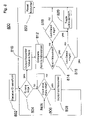
- PLL system 100 includes Phase/Frequency Detector (PFD) with High Precision Lock Detector 102 .
- PFD Phase/Frequency Detector
- the PFD with High Precision Lock Detector 102 receives a reference frequency f 1 signal and a feedback frequency f 2 signal.
- Reference frequency f 1 signal may be generated externally by an oscillator, such as a quartz crystal (not shown).
- the reference frequency is generally a lower frequency multiple of the desired lock frequency.
- the feedback frequency f 2 signal is the VCO output feedback frequency, which is first divided down by frequency divider 112 .
- PLL system 100 further includes charge pump 104 that receives up/down pulses from PFD with High Precision Lock Detector 102 .
- Charge Pump 104 provides an analog voltage, designated as voltage tuning one, or VT 1 , to RC filter network 106 .
- the VT 1 signal controls the frequency output of VCO 108 .
- Charge pump 104 also receives an Enable 1 signal for enabling or disabling the charge pump. This signal is described in more detail below.
- the PLL system 100 also includes a second phase/frequency detector (PFD) with a charge pump, shown as 110 .
- the PFD with charge pump 110 (abbreviated herein as PFDCP 110 ) provides an analog voltage, designated as voltage tuning two, or VT 2 , to RC filter network 106 .
- the VT 2 signal controls the frequency output of VCO 108 .
- the PFDCP 110 receives an Enable 2 signal for enabling or disabling the charge pump of PFDCP 110 .
- the Enable 2 signal is described in more detail below.
- the VCO 108 provides as an output the VCO OUT signal, typically at a high frequency (for example 10 GHz). This high frequency may or may not be the desired frequency.
- the VCO OUT signal is looped back as a feedback signal to frequency divider 112 and to PFDCP 110 .
- Frequency divider 112 divides the VCO OUT frequency by an integer multiple (for example, divide by 64) and provides the divided VCO OUT signal as the feedback frequency f 2 signal (for example 150 MHz).
- PFDCP 110 receives the VCO OUT signal directly from VCO 108 and the frequency divider is bypassed.
- the frequency of the VCO OUT signal may be, for example, 10 GHz.
- the PFDCP 110 also receives a reference frequency f 5 signal, which is the desired high frequency VCO output signal that PLL system 100 is attempting to lock onto.
- a reference frequency f 5 signal may be 10 GHz.
- the reference frequency f 4 signal may be the VCO OUT signal directly connected to PFDCP 110 or, alternatively, the f 4 signal may be derived from the VCO OUT signal through frequency divider 112 .
- Frequency divider 112 may divide the VCO OUT frequency by an integer multiple (for example, divide by 2) and provide the divided VCO OUT signal as the feedback frequency f 4 signal (for example 5 GHz).
- PFDCP 110 may receive the VCO OUT signal directly from VCO 108 .
- the frequency of the VCO OUT signal may be, for example, 10 GHz.
- the RC filter network 106 includes R 1 and C 1 connected in series to each other and in parallel to the terminal providing the VT 1 tuning signal. Similarly, RC filter network 106 includes R 3 and C 2 connected in series to each other and in parallel to the terminal providing the VT 2 tuning signal. A resistor R 2 couples the output of the VT 1 signal together with the output of the VT 2 signal.
- charge pump 104 may be in a disabled mode, nevertheless the VT 1 signal is still present, and effectively supplies a DC bias about which the VT 2 signal primarily controls the VCO frequency.
- PFDCP 110 may be in a disabled mode, nevertheless the VT 2 signal is still present, but effectively provides minor affect on controlling the VCO frequency, because primary control is provided by way of the VT 1 signal.
- VT 1 signal and the VT 2 signal are combined by way of RC filter network 106 and both tuning signals simultaneously control the frequency of the VCO output signal.
- the amount of control varies depending on whether one charge pump is enabled or the other charge pump is enabled. As described previously, only one charge pump at any one time is enabled, while the other charge pump is disabled. Because both VT 1 and VT 2 remain in the direct path of tuning the VCO, this effectively reduces noise in the system, although the system switches from one charge pump to the other charge pump.
- PFD with High Precision Lock Detector 102 includes Phase/Frequency detector (PFD) 202 , which receives the signals having the reference and feedback frequencies f 1 and f 2 , respectively.
- the PFD 202 receives the reference frequency f 1 signal and the feedback frequency f 2 signal and generates, in a conventional manner, output pulses labeled as down (DN) and up bar (UPB), which are used to control Charge Pump 104 shown in FIG. 1 .
- Signals DN and UPB are, at the same time, provided to a logic gate, exclusive-NOR gate 204 (XNOR 204 ).
- XNOR exclusive-NOR gate
- the XNOR provides the XNOR OUT signal, as shown.
- the XNOR OUT signal is integrated by low pass filter (LPF) 206 , which generates an LPF OUT signal.
- LPF OUT signal is compared to a predetermined reference threshold voltage, VREF, by comparator 208 .
- Comparator 208 generates output signal f 3 , which is provided to frequency offset analyzer 210 .
- Frequency offset analyzer 210 generates the LOCK DETECT signal, which is also shown in FIG. 1 as the LOCK DETECT signal outputted from PFD with High Precision Lock Detector 102 .
- FIG. 3 there is shown an exemplary embodiment of the PFD with High Precision Lock Detector that has just been described with reference to FIG. 2 .
- the logic gates of a conventional phase/frequency detector are shown as PFD 202 .
- This PFD is known as a zero dead zone PFD for generating up (actually up bar) and down pulses.
- the PFD 202 is followed by XNOR gate 204 and low pass filter (LPF) 206 , the latter being implemented, as an example, by resistor R 4 and capacitor C 3 .
- the output from the LPF is inputted into comparator 208 for comparison with the VREF signal.
- the output signal from comparator 208 shown as the f 3 signal, is provided to Frequency Offset Analyzer 210 .
- output pulse DN is generally low and output pulse UPB is generally high; each of these pulses is seen as a transient toggle pulse.
- VCO feedback frequency f 2 begins to lag reference frequency f 1
- output pulse DN remains generally low, and the duration of time that output pulse UPB is low increases proportionally to the increase in the lag time.
- VCO feedback frequency f 2 begins to lead reference frequency f 1
- output pulse UPB remains generally high, and the duration of time that output pulse DN is high increases proportionally to the increase in the lead time.
- output pulses UPB and DN are proportional to the frequency and phase difference between the two f 1 and f 2 input signals.
- This proportionality of the output pulses UPB and DN to the phase and frequency of input signals f 1 and f 2 is utilized to control the output frequency of the VCO.
- Output pulses UPB and DN are connected to charge pump 104 which increases or decreases the VCO control voltage based on output pulses UPB and DN.
- charge pump 104 increases the VCO control voltage; and as the pulse duration of output pulse DN become increasingly, as a function of time, to be in a high state, charge pump 104 decreases the VCO control voltage.
- output pulses UPB and DN are inputted into exclusive-NOR gate 204 . Because output pulse UPB is proportional to the phase and frequency lag of f 2 to f 1 , and output pulse DN is proportional to the phase and frequency lead of f 2 to f 1 , the output of the exclusive-NOR is also proportional to the phase and frequency difference between f 1 and f 2 .
- the XNOR OUT signal is integrated by low pass filter 206 , forming a low pass average analog voltage level at LPF OUT.
- the LPF OUT is then compared to a predetermined reference voltage threshold, VREF, by comparator 208 .
- the VREF threshold is determined based on the UPB and DN pulse amplitudes and the low pass filter characteristics.
- comparator 208 toggles its output to provide the f 3 signal.
- the f 3 signal becomes a level one when the voltage of LPF OUT exceeds VREF and a level zero when the voltage of LPF OUT is lower than VREF.
- FIGS. 4A-G show exemplary relationships among these signals.
- the f 1 and f 2 signals are depicted in FIGS. 4A and 4B .
- the output pulses UPB and DN are depicted, respectively, in FIGS. 4C and 4D .
- the XNOR OUT signal is shown in FIG. 4E .
- the integrated output of LPF OUT is shown against the VREF threshold in FIG. 4F
- the f 3 output signal of comparator 208 is shown in FIG. 4G .
- Frequency offset analyzer 210 is provided to frequency offset analyzer 210 , as shown in FIG. 5 .
- Frequency offset analyzer 210 may be implemented in hardware, or may be implemented as an embedded software routine executed in a microcontroller, or may be a combination of both.
- Frequency offset analyzer 210 includes rising edge is detector 502 , which receives the f 3 signal and marks its positive pulse transition. When the f 3 signal has a positive pulse transition, rising edge detector 502 toggles the RST (reset) signal.
- RST reset
- Ncounter 504 receives the RST signal and an Nclk signal.
- the RST signal is used to reset Ncounter 504 , while the Nclk signal may be a system clock.
- Ncounter 504 counts the number of Nclk transitions between the rising edges of the RST signal, and outputs a counter value of Ncnt. Because the RST signal corresponds to the rising edges of the f 3 signal, the value of Ncnt is effectively a measure of the period of the f 3 signal.
- T 1/(f 1 ⁇ f 2 ).
- the Ncnt value is compared to a predetermined threshold count value of Nthreshold by comparator 506 . If the Ncnt value exceeds the Nthreshold value, comparator 506 provides a CMP output signal to XOR 507 and toggle logic 508 . If control signal LOCK DETECT is in a low state and the CMP output becomes high, then LOCK DETECT is toggled into a high state, indicating that the PLL is locked on correctly to the desired frequency. If, on the other hand, control signal LOCK DETECT is in a high state and the CMP output becomes high, then LOCK DETECT is maintained in its high state, indicating that the PLL is still locked on correctly to the desired frequency. If, however, control signal LOCK DETECT is in a high state and the CMP output becomes low, then LOCK DETECT is toggled into a low state, indicating that the PLL has lost lock to the desired frequency.
- FIG. 8 shows an exemplary method 800 for controlling the LOCK DETECT signal provided from the frequency offset analyzer of FIG. 5 .
- rising edge detector 502 receives the f 3 signal (waveform), and waits for a rising edge to be detected on the f 3 signal.
- Decision block 804 remains false until a rising edge is detected. So long as decision block 804 is false, the method sequentially enters decision blocks 806 and 808 .
- Ncounter 504 is incremented one count for every clock cycle of Nclk, thus counting the number of Nclk values between a previous rising edge of the f 3 waveform until detection of a current rising edge of the f 3 waveform by decision block 804 .
- Ncnt is compared to a predetermined number, Nthreshold, in process block 812 and decision block 814 .
- the number Nthreshold represents the minimum number of Nclk cycles between f 3 rising edges for PLL 100 to be considered to have a locked status.
- Nthreshold is selected to meet a predetermined ppm tolerance level for the frequency accuracy of PLL 100 .
- Ncnt exceeds Nthreshold
- decision block 814 becomes true, and PLL 100 is in a locked status. If PLL 100 is in a locked status, the LOCK DETECT output is set high (assuming that it is not already set high) by way of decision block 816 and process block 820 . If, however, the LOCK DETECT signal is already high (as determined by decision block 818 ), then the method does not reset the LOCK DETECT signal and only loops back to reset the Ncounter by way of process block 822 .
- Ncnt is less than Nthreshold, however, as determined by decision block 814 , the method loops to decision block 818 to determine whether the LOCK DETECT signal is high. If the LOCK DETECT signal is high, then the method enters process block 820 to toggle the LOCK DETECT signal to false. The method loops back to reset the Ncounter by way of process block 822 . Process block 822 resets the value of the Ncounter to zero, and the method returns to decision block 804 to detect the next rising edge of the f 3 waveform.
- FIGS. 9A-9C show exemplary relationships among UPB, DN and XNOR OUT, when reference frequency f 1 is less than VCO feedback frequency f 2 .
- the UPB pulse is a transient and the DN pulse is proportional to the phase/frequency difference between the f 1 and f 2 signals.
- FIGS. 10A-10C show other exemplary relationships among UPB, DN and XNOR OUT, when reference frequency f 1 is greater than VCO feedback frequency f 2 .
- the DN pulse is a transient and the UPB pulse is proportional to the phase/frequency difference between the f 1 and f 2 signals.
- PLL 100 has two modes, an acquisition mode and a tracking mode.
- charge pump 104 is enabled by the Enable 1 signal.
- the Enable 1 signal may be a control signal from an external circuit, such as a microcontroller.
- the charge pump of PFDCP 110 is enabled by the Enable 2 signal.
- the Enable 2 signal may be another control signal from an external circuit, such as a microcontroller.
- the decision whether to assert the Enable 1 signal or the Enable 2 signal is based upon the status of the LOCK DETECT output from PFD with High Precision Lock Detector 102 . It will be appreciated that the Enable 1 and Enable 2 signals are mutually exclusive because they cannot be asserted at the same time.
- tuning voltage V 11 that controls VCO 108 has a high gain, such as 1 GHz/Volt, and tuning voltage VT 2 has a lower gain, such as 300 MHz/Volt.
- the present invention uses charge pump 104 to primarily control the high gain of tuning voltage VT 1 , and to secondarily control the lower gain of tuning voltage VT 2 .
- the charge pump of PFDCP 110 is used to primarily fine tune the VCO by way of the low gain of tuning voltage VT 2 and tuning voltage VT 1 has minimal impact on the frequency of the VCO. This advantageously minimizes the noise of the VCO output signal.
- the present invention controls the affect of tuning voltages V 11 and VT 2 on the VCO by way of filter network 106 .
- the filter network is comprised of three resistors and two capacitors.
- the combination of R 1 and C 1 approximately defines the bandwidth of PLL 100 when charge pump 104 is enabled in the acquisition mode.
- Resistor R 2 transfers the voltage between VT 1 to VT 2 .
- the combination of R 3 and C 2 approximately defines the bandwidth of PLL 100 when the charge pump of PFDCP 110 is operational in the tracking mode.
- V 12 When V 12 is active, little current is passed through R 2 and R 1 to have any appreciable affect on VT 1 . In this manner, V 11 is effective in supplying a DC bias to the VCO and small frequency shift occurs when VT 2 is enabled and VT 1 is disabled.
- the extra filtering of VT 2 by filter network 106 helps dampen the response of VCO 108 and reduces frequency overshoot.
- Exemplary values for the elements of filter network 106 may be as follows: the R 1 , R 2 and R 3 values may, respectively, be 20K, 10K and 4K; the C 1 and C 2 values may each be 20 pfd.
- the present invention has another advantage over the prior art. Because PFD with High Precision Lock Detector 102 operates at low input frequencies of f 1 and f 2 (such as in the range of 150 MHz), charge pump 104 does not need to have a high response speed, and may be implemented by an inexpensive charge pump.
- tuning voltage VT 1 has a high gain, such as 1 GHz/Volt
- tuning voltage VT 2 has a lower gain, such as 300 MHz/Volt.
- PFDCP 110 directly control the lower gain tuning voltage VT 2 , but indirectly maintain the DC voltage level of the high gain tuning voltage VT 1 . This operation further reduces PLL noise.
- PFDCP 110 operates at the higher frequencies of f 4 and f 5 , which in the present embodiment are in the range of 10 GHz, PFDCP 110 needs to have high response speed and, as such, may be implemented by a high frequency Hodge linear PFD and charge pump.
Landscapes
- Stabilization Of Oscillater, Synchronisation, Frequency Synthesizers (AREA)
Abstract
Description
T=1/(reference frequency−VCO feedback frequency)
where the reference frequency is the frequency of the reference signal, and the VCO feedback frequency is the frequency of the VCO output signal. When T exceeds the predetermined threshold time period, the VCO is providing the desired frequency for the VCO output signal.
Claims (22)
T=1/(reference frequency−VCO feedback frequency)
T=1/(reference frequency−VCO feedback frequency)
Priority Applications (4)
| Application Number | Priority Date | Filing Date | Title |
|---|---|---|---|
| US11/485,664 US7420428B2 (en) | 2006-07-13 | 2006-07-13 | Low noise phase locked loop with a high precision lock detector |
| AU2007202856A AU2007202856B8 (en) | 2006-07-13 | 2007-06-20 | Low noise phase locked loop with a high precision lock detector |
| DE602007005733T DE602007005733D1 (en) | 2006-07-13 | 2007-07-03 | Low noise phase locked loop with high precision shutter detector |
| EP07111599A EP1885067B1 (en) | 2006-07-13 | 2007-07-03 | Low noise phase locked loop with high precision lock detector |
Applications Claiming Priority (1)
| Application Number | Priority Date | Filing Date | Title |
|---|---|---|---|
| US11/485,664 US7420428B2 (en) | 2006-07-13 | 2006-07-13 | Low noise phase locked loop with a high precision lock detector |
Publications (2)
| Publication Number | Publication Date |
|---|---|
| US20080024230A1 US20080024230A1 (en) | 2008-01-31 |
| US7420428B2 true US7420428B2 (en) | 2008-09-02 |
Family
ID=38562854
Family Applications (1)
| Application Number | Title | Priority Date | Filing Date |
|---|---|---|---|
| US11/485,664 Active 2026-10-20 US7420428B2 (en) | 2006-07-13 | 2006-07-13 | Low noise phase locked loop with a high precision lock detector |
Country Status (4)
| Country | Link |
|---|---|
| US (1) | US7420428B2 (en) |
| EP (1) | EP1885067B1 (en) |
| AU (1) | AU2007202856B8 (en) |
| DE (1) | DE602007005733D1 (en) |
Cited By (3)
| Publication number | Priority date | Publication date | Assignee | Title |
|---|---|---|---|---|
| US20070194811A1 (en) * | 2003-12-19 | 2007-08-23 | Koninklijke Philips Electronic, N.V. | Method and arrangement for interference compensation in a voltage-controlled frequency generator |
| US20090189657A1 (en) * | 2008-01-25 | 2009-07-30 | Himax Technologies Limited | Delay locked loop circuit and method for eliminating jitter and offset therein |
| US20110006820A1 (en) * | 2009-07-07 | 2011-01-13 | Mstar Semiconductor, Inc. | Dual Phase-Locked Loop Circuit and Method for Controlling the Same |
Families Citing this family (10)
| Publication number | Priority date | Publication date | Assignee | Title |
|---|---|---|---|---|
| US7990224B2 (en) * | 2007-04-27 | 2011-08-02 | Atmel Corporation | Dual reference phase tracking phase-locked loop |
| US8228431B2 (en) * | 2009-08-31 | 2012-07-24 | Silicon Laboratories Inc. | Digital phase lock loop configurable as a frequency estimator |
| GB2498945A (en) * | 2012-01-31 | 2013-08-07 | Texas Instruments Ltd | Improved loop filter for phase locked loop (PLL) |
| EP3258603B1 (en) * | 2016-06-15 | 2022-11-09 | Nxp B.V. | Phase locked loop with lock/unlock detector |
| CN109274367A (en) * | 2018-09-05 | 2019-01-25 | 东南大学 | A phase detector which is resistant to charge pump mismatch and phase-locked loop pull-in range |
| CN109358228B (en) * | 2018-11-09 | 2020-12-15 | 哈工大(张家口)工业技术研究院 | Real-time estimation method of positive and negative sequence components of grid voltage based on double enhanced phase-locked loop |
| TWI695585B (en) * | 2019-07-31 | 2020-06-01 | 力林科技股份有限公司 | Pulse width modulation control circuit and control method of pulse width modulation signal |
| JP2023548568A (en) * | 2020-12-08 | 2023-11-17 | アナログ ディヴァイスィズ インク | External oscillator control and calibration |
| KR20230094575A (en) * | 2021-12-21 | 2023-06-28 | 주식회사 엘엑스세미콘 | Frequency generator and frequency correction method of frequency generator |
| CN117978160A (en) * | 2024-03-29 | 2024-05-03 | 成都电科星拓科技有限公司 | A frequency discrimination circuit and clock data recovery chip |
Citations (4)
| Publication number | Priority date | Publication date | Assignee | Title |
|---|---|---|---|---|
| US4542351A (en) | 1981-09-08 | 1985-09-17 | Fujitsu Limited | PLL for regenerating a synchronizing signal from magnetic storage |
| EP0278079A2 (en) | 1987-02-11 | 1988-08-17 | International Business Machines Corporation | NRZ Phase-locked loop circuit with associated monitor and recovery circuitry |
| US6803827B1 (en) * | 2003-04-09 | 2004-10-12 | Analog Devices, Inc. | Frequency acquisition system |
| US6856202B2 (en) | 2003-04-14 | 2005-02-15 | Wolfson Microelectronics, Plc | Phase/frequency detector and phase lock loop circuit |
-
2006
- 2006-07-13 US US11/485,664 patent/US7420428B2/en active Active
-
2007
- 2007-06-20 AU AU2007202856A patent/AU2007202856B8/en not_active Ceased
- 2007-07-03 EP EP07111599A patent/EP1885067B1/en not_active Not-in-force
- 2007-07-03 DE DE602007005733T patent/DE602007005733D1/en active Active
Patent Citations (4)
| Publication number | Priority date | Publication date | Assignee | Title |
|---|---|---|---|---|
| US4542351A (en) | 1981-09-08 | 1985-09-17 | Fujitsu Limited | PLL for regenerating a synchronizing signal from magnetic storage |
| EP0278079A2 (en) | 1987-02-11 | 1988-08-17 | International Business Machines Corporation | NRZ Phase-locked loop circuit with associated monitor and recovery circuitry |
| US6803827B1 (en) * | 2003-04-09 | 2004-10-12 | Analog Devices, Inc. | Frequency acquisition system |
| US6856202B2 (en) | 2003-04-14 | 2005-02-15 | Wolfson Microelectronics, Plc | Phase/frequency detector and phase lock loop circuit |
Cited By (6)
| Publication number | Priority date | Publication date | Assignee | Title |
|---|---|---|---|---|
| US20070194811A1 (en) * | 2003-12-19 | 2007-08-23 | Koninklijke Philips Electronic, N.V. | Method and arrangement for interference compensation in a voltage-controlled frequency generator |
| US7498888B2 (en) * | 2003-12-19 | 2009-03-03 | Nxp B.V. | Method and arrangement for interference compensation in a voltage-controlled frequency generator |
| US20090189657A1 (en) * | 2008-01-25 | 2009-07-30 | Himax Technologies Limited | Delay locked loop circuit and method for eliminating jitter and offset therein |
| US7733139B2 (en) * | 2008-01-25 | 2010-06-08 | Himax Technologies Limited | Delay locked loop circuit and method for eliminating jitter and offset therein |
| US20110006820A1 (en) * | 2009-07-07 | 2011-01-13 | Mstar Semiconductor, Inc. | Dual Phase-Locked Loop Circuit and Method for Controlling the Same |
| US8564340B2 (en) * | 2009-07-07 | 2013-10-22 | Mstar Semiconductor, Inc. | Dual phase-locked loop circuit and method for controlling the same |
Also Published As
| Publication number | Publication date |
|---|---|
| DE602007005733D1 (en) | 2010-05-20 |
| EP1885067B1 (en) | 2010-04-07 |
| US20080024230A1 (en) | 2008-01-31 |
| EP1885067A2 (en) | 2008-02-06 |
| AU2007202856A1 (en) | 2008-01-31 |
| EP1885067A3 (en) | 2008-02-20 |
| AU2007202856B2 (en) | 2011-07-14 |
| AU2007202856B8 (en) | 2011-11-10 |
Similar Documents
| Publication | Publication Date | Title |
|---|---|---|
| AU2007202856B8 (en) | Low noise phase locked loop with a high precision lock detector | |
| US7372339B2 (en) | Phase lock loop indicator | |
| US8736323B2 (en) | Method and apparatus for on-chip phase error measurement to determine jitter in phase-locked loops | |
| US6816019B2 (en) | Automatically calibrated phase locked loop system and associated methods | |
| CA2220622C (en) | Method and circuit for built in self test of phase locked loops | |
| US6466058B1 (en) | PLL lock detection using a cycle slip detector with clock presence detection | |
| KR100918355B1 (en) | Apparatus and method for controlling delay locked loop or phase locked loop as a function of loop frequency | |
| KR100545947B1 (en) | Phase locked loop | |
| US7277518B2 (en) | Low-jitter charge-pump phase-locked loop | |
| US7663417B2 (en) | Phase-locked loop circuit | |
| US6496554B1 (en) | Phase lock detection circuit for phase-locked loop circuit | |
| EP1158680B1 (en) | Phase comparator and clock recovery circuit | |
| US6998889B2 (en) | Circuit, apparatus and method for obtaining a lock state value | |
| US6396890B1 (en) | Phase corrected frequency synthesizers | |
| US7719368B1 (en) | Configurable reset circuit for a phase-locked loop | |
| US7567642B2 (en) | Phase detector with extended linear operating range | |
| US6696828B2 (en) | Integrated circuit and lot selection system therefor | |
| US7432749B1 (en) | Circuit and method for improving frequency range in a phase locked loop | |
| US8508271B1 (en) | Phase locked loop | |
| US7598816B2 (en) | Phase lock loop circuit with delaying phase frequency comparson output signals | |
| JP7120155B2 (en) | Anomaly detector | |
| JP3647699B2 (en) | Integrated circuit and lot sorting system | |
| US7327199B1 (en) | Phase-locked loop (PLL) device and method for entering a test mode without a dedicated test pin | |
| US7171318B2 (en) | PLL filter leakage sensor | |
| JP3532490B2 (en) | Lock detector and phase locked loop circuit using the same |
Legal Events
| Date | Code | Title | Description |
|---|---|---|---|
| AS | Assignment |
Owner name: ITT MANUFACTURING ENTERPRISES, INC., DELAWARE Free format text: ASSIGNMENT OF ASSIGNORS INTEREST;ASSIGNORS:PERA, FLORIN;WHITTAKER, DENNIS;REEL/FRAME:018059/0059 Effective date: 20060712 |
|
| STCF | Information on status: patent grant |
Free format text: PATENTED CASE |
|
| AS | Assignment |
Owner name: EXELIS INC., VIRGINIA Free format text: ASSIGNMENT OF ASSIGNORS INTEREST;ASSIGNOR:ITT MANUFACTURING ENTERPRISES LLC (FORMERLY KNOWN AS ITT MANUFACTURING ENTERPRISES, INC.);REEL/FRAME:027574/0040 Effective date: 20111221 |
|
| AS | Assignment |
Owner name: EXELIS, INC., VIRGINIA Free format text: ASSIGNMENT OF ASSIGNORS INTEREST;ASSIGNOR:ITT MANUFACTURING ENTERPRISES, LLC (FORMERLY KNOWN AS ITT MANUFACTURING ENTERPRISES, INC.);REEL/FRAME:027604/0001 Effective date: 20111028 |
|
| FPAY | Fee payment |
Year of fee payment: 4 |
|
| FPAY | Fee payment |
Year of fee payment: 8 |
|
| AS | Assignment |
Owner name: HARRIS CORPORATION, FLORIDA Free format text: MERGER;ASSIGNOR:EXELIS INC.;REEL/FRAME:039362/0534 Effective date: 20151223 |
|
| AS | Assignment |
Owner name: HARRIS GLOBAL COMMUNICATIONS, INC., NEW YORK Free format text: CHANGE OF NAME;ASSIGNOR:HARRIS SOLUTIONS NY, INC.;REEL/FRAME:047598/0361 Effective date: 20180417 Owner name: HARRIS SOLUTIONS NY, INC., NEW YORK Free format text: ASSIGNMENT OF ASSIGNORS INTEREST;ASSIGNOR:HARRIS CORPORATION;REEL/FRAME:047600/0598 Effective date: 20170127 |
|
| MAFP | Maintenance fee payment |
Free format text: PAYMENT OF MAINTENANCE FEE, 12TH YEAR, LARGE ENTITY (ORIGINAL EVENT CODE: M1553); ENTITY STATUS OF PATENT OWNER: LARGE ENTITY Year of fee payment: 12 |