US7382183B2 - Minimizing switching noise and its effects in auto-zeroed amplifiers - Google Patents
Minimizing switching noise and its effects in auto-zeroed amplifiers Download PDFInfo
- Publication number
- US7382183B2 US7382183B2 US11/774,648 US77464807A US7382183B2 US 7382183 B2 US7382183 B2 US 7382183B2 US 77464807 A US77464807 A US 77464807A US 7382183 B2 US7382183 B2 US 7382183B2
- Authority
- US
- United States
- Prior art keywords
- nulling
- amplifier
- differential
- auxiliary
- inputs
- Prior art date
- Legal status (The legal status is an assumption and is not a legal conclusion. Google has not performed a legal analysis and makes no representation as to the accuracy of the status listed.)
- Active
Links
Images


Classifications
-
- H—ELECTRICITY
- H03—ELECTRONIC CIRCUITRY
- H03F—AMPLIFIERS
- H03F3/00—Amplifiers with only discharge tubes or only semiconductor devices as amplifying elements
- H03F3/45—Differential amplifiers
- H03F3/45071—Differential amplifiers with semiconductor devices only
- H03F3/45479—Differential amplifiers with semiconductor devices only characterised by the way of common mode signal rejection
- H03F3/45928—Differential amplifiers with semiconductor devices only characterised by the way of common mode signal rejection using IC blocks as the active amplifying circuit
- H03F3/45968—Differential amplifiers with semiconductor devices only characterised by the way of common mode signal rejection using IC blocks as the active amplifying circuit by offset reduction
- H03F3/45982—Differential amplifiers with semiconductor devices only characterised by the way of common mode signal rejection using IC blocks as the active amplifying circuit by offset reduction by using a feedforward circuit
- H03F3/45986—Differential amplifiers with semiconductor devices only characterised by the way of common mode signal rejection using IC blocks as the active amplifying circuit by offset reduction by using a feedforward circuit using switching means, e.g. sample and hold
Definitions
- the present disclosure relates to integrated circuit operational amplifiers, and more particularly, to an integrated circuit auto-zeroed operational amplifier having minimized switching noise.
- Auto-zeroed operational amplifiers are a class of analog circuits that combine analog and digital (switching) circuitry resulting in very low input-referred DC offset and noise. These operational amplifiers are often used in precision applications where high gain is necessary to resolve very small voltages. Examples include RTD, thermocouple, resistive current measurement and other sensing applications.
- the use of an auto-zeroed operational amplifier may relax the accuracy requirements of the A/D converter, saving cost.
- Today's auto-zeroed operational amplifiers bear little resemblance to the early chopping schemes that were used to reduce the average offsets. Those circuits were very simple using discrete amplifiers and switches to chop the amplifier's inputs and outputs using a clock. Heavy filtering was required to achieve low offset, and filter out the switching noise.
- Chopper amplifiers had a low frequency bandwidth, usually a few Hertz, limited by the large settling time constants.
- Another scheme uses chopper stabilization of a wideband amplifier and a chopper amplifier.
- the chopper amplifier was used to “stabilize” or reduce the DC offset error of the wideband amplifier. Higher operating bandwidths were thereby achieved, but these chopped circuits had high output noise and required additional output signal filtering to be practical.
- a single nulling amplifier is used to compensate for the “main” (continuous) amplifier.
- the null amplifier is disconnected from the main amplifier, and the correction voltage is held on the main auxiliary port by a storage capacitor.
- This approach causes the open-loop gain to change between the compensation and nulling cycles because during the compensation cycle the total gain is the cascade of the null and main amplifiers while during the zeroing cycle the gain is that of just the main amplifier. This causes low frequency distortion (ripple) to appear at the output at multiples of the sampling frequency.
- a second null amplifier is added so as to compensate the main amplifier while the first null amplifier is being zeroed. This maintains the open-loop gain relatively constant, reducing the distortion inherent in the prior technology.
- a further improvement is that the timing of the switch operations between the two null amplifiers and the main amplifier is designed have a make-before-break overlap. This ensures that the main amplifier is continuously driven by one or both null amplifiers, maintaining a low impedance at the main amplifier auxiliary port and reducing the glitch energy at the output.
- a small flywheel capacitor may be added to further reduce the glitch magnitude. Two pair of zeroing switches are used, one for each null amplifier. By connecting one pair of zeroing switches opposite to the other, the glitch energy will tend to average out.
- the null amplifiers are implemented using a fully-differential topology. With two null amplifiers in the system, these may not have the same common-mode voltage due to transistor mismatches in their internal common-mode feedback loops. This can present a new source of glitching because the main auxiliary port “sees” a sharp change in common-mode when the null amplifiers switch. Therefore, a common-mode zeroing loop is included in addition to the normal differential mode zeroing loop so that both null amplifiers have approximately the same common-mode voltage. Zeroing of the two loops is done concurrently so no additional delay is incurred.
- the null amplifier differential mode error (offset) is zeroed, then used to correct the main amplifier offset. Mismatches between the main and null amplifiers may cause glitches when the null amplifier is connected to the main auxiliary port. This is because at the end of the zeroing cycle the null amplifier output voltage may not the same as what the main auxiliary port needs to correct the main amplifier offset.
- DM differential mode
- CM common-mode
- an auto-zeroing differential amplifier may comprise: a main amplifier having differential inputs, differential outputs, and an auxiliary port having differential inputs; a first nulling amplifier configured for differential and common mode self correction, the first nulling amplifier having differential inputs and outputs; a second nulling amplifier configured for differential and common mode self correction, the second nulling amplifier having differential inputs and outputs; first nulling amplifier input zeroing switches coupled to the main amplifier differential inputs and the first nulling amplifier differential inputs, wherein the first nulling amplifier input zeroing switches are used during offset zeroing of the main amplifier by the first nulling amplifier; second nulling amplifier input zeroing switches coupled to the main amplifier differential inputs and the second nulling amplifier differential inputs, wherein the second nulling amplifier input zeroing switches are used during offset zeroing of the main amplifier by the second nulling amplifier; first nulling amplifier output switches coupled between the first nulling amplifier differential outputs and the main amplifier auxiliary port differential inputs, wherein the first nulling amplifier output switches couple the first nulling amplifier differential outputs to
- a method of minimizing switching noise in auto-zeroed amplifiers may comprise the steps of: providing a main amplifier having differential signal inputs and outputs, and differential auxiliary inputs; providing first and second nulling amplifiers having differential signal inputs, differential outputs and differential auxiliary inputs, wherein the differential signal inputs and differential outputs are switchably coupled to the main amplifier differential signal inputs and differential auxiliary inputs; nulling a differential mode (DM) offset error of the main amplifier by: storing the DM offset error in first and second DM offset error capacitors coupled to the first and second nulling amplifiers, respectively, and applying the stored DM offset error to the main amplifier differential auxiliary inputs; nulling a common mode (CM) offset error of the main amplifier by sampling the CM offset error, storing the CM offset error in first and second CM offset error capacitors coupled to the first and second nulling amplifiers, respectively, and applying the stored CM offset error to the main amplifier differential auxiliary inputs; and precharging the first and second nulling DM
- FIG. 1 illustrates a schematic block diagram of a prior technology auto-zeroed operational amplifier
- FIG. 2 illustrates a schematic block diagram of an auto-zeroed operational amplifier, according to a specific example embodiment of this disclosure
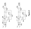
- FIG. 3 illustrates schematic diagrams of the first and second nulling amplifiers implemented using a fully-differential topology, according to the specific example embodiment shown in FIG. 2 ;
- FIGS. 4( a ), 4 ( b ) and 4 ( c ) illustrate schematic timing diagrams showing transient (“glitch”) behavior of a prior technology auto-zeroed operational amplifier during offset correction;
- FIG. 4( d ) illustrates a schematic timing diagram showing transient (“glitch”) behavior of a case where both nulling amplifier outputs are pre-charged to match the expected main auxiliary port voltage before switching nulling amplifiers;
- FIG. 4( e ) illustrates a schematic timing diagram showing transient (“glitch”) behavior where both pre-charging and common-mode zeroing are used to reduce output glitches, according to a specific example embodiment of this disclosure
- FIG. 5 illustrates a more detailed schematic block diagram of the nulling amplifiers shown in FIG. 2 , according to a specific example embodiment of this disclosure.
- FIG. 6 illustrates timing diagrams for the operation of the auto-zeroed operational amplifier and nulling amplifiers shown in FIG. 5 , according to a specific example embodiment of this disclosure.
- the prior technology auto-zeroed amplifier may comprise at least two amplifiers 102 and 104 that are combined to generate the final signal output.
- a conventional wide bandwidth “main” amplifier 102 is connected directly from input to output and continuously processes the incoming signal.
- a second, very high gain “nulling” amplifier 104 is connected in parallel for offset correction.
- the amplifier 104 is zeroed to null its own offset and to eliminate low frequency 1/f noise below the chopping frequency. Zeroing involves shorting together the two inputs of the amplifier 104 with switch 114 and storing the resulting offset onto a capacitor 108 .
- this correction voltage is applied to the nulling amplifier 104 through an auxiliary port 118 .
- the correction voltage is held on the main auxiliary port 120 by a storage capacitor 106 when the nulling amplifier 104 is disconnected from the main amplifier 102 during its zeroing cycle. This correction voltage is then used to null the offset of the main amplifier 102 through another auxiliary port 120 .
- the auto-zeroed operational amplifier may comprise a main amplifier 202 , a first nulling amplifier 208 , a second nulling amplifier 218 , switches 206 , 210 , 216 , 220 and 222 ; and capacitors 232 , 234 and 236 .
- the second nulling amplifier 218 compensates the main amplifier 202 while the first nulling amplifier 208 is being zeroed. This maintains the open-loop gain relatively constant, reducing the distortion present in the prior technology.
- a further improvement is that the operational timing of the switches 206 , 210 , 216 , 220 and 222 between the first nulling amplifier 208 , the second nulling amplifier 218 , and the main amplifier 202 function with a make-before-break overlap. This ensures that the main amplifier 202 is continuously driven by one or both of the nulling amplifiers 208 and 218 , thus maintaining a low impedance at the main amplifier auxiliary port 242 , and also reducing the glitch energy at the output 244 .
- a flywheel capacitor 232 may be added to further reduce the glitch magnitude. Two pair of zeroing switches 206 and 216 are used, one pair for each of the nulling amplifiers 208 and 218 , respectively.
- FIG. 3 depicted are schematic diagrams of the first and second nulling amplifiers implemented using a fully-differential topology, according to the specific example embodiment shown in FIG. 2 .
- the first and second nulling amplifiers 208 and 218 are implemented using a fully-differential topology.
- one zeroing switch pair e.g., switches 206 a and 206 b
- the other zeroing switch pair e.g., switches 216 a and 216 b
- first and second nulling amplifiers 208 and 218 may not have the same common-mode voltage due to transistor mismatches in their internal common-mode feedback loops. This may present a source of glitching (e.g., unwanted transient noise) because the main auxiliary port 242 of the main amplifier 202 may “see” a sharp change in common-mode voltage when the first and second nulling amplifiers 208 and 218 , respectively, are switched between the auxiliary port 242 .
- these glitches may be substantially reduced by adding a common-mode zeroing loop in addition to the normal differential mode zeroing loop so that the first and second nulling amplifiers 208 and 218 , respectively, have approximately the same common-mode voltage.
- One of the nulling amplifiers is being zeroed while the other nulling amplifier is connected to the auxiliary port 242 . Thus, zeroing of the two loops is done concurrently so no additional delay is incurred.
- the correction voltage required on the auxiliary port 242 may not be equal to the nulling amplifier output voltage when the nulling amplifier is connected to the auxiliary port 242 .
- This is another source of glitching because the auxiliary port 242 of the main amplifier 202 may “see” a sharp change in differential-mode voltage when the nulling amplifiers 208 or 218 are connected to the auxiliary port 242 .
- these glitches may be substantially reduced by adding a pre-charge operation to adjust the nulling amplifier output voltage to substantially match the required nulling correction voltage on the auxiliary port 242 prior to connecting the nulling amplifer to the auxiliary port 242 .
- prior technology auto-zeroed amplifiers e.g., FIG. 1
- the nulling amplifier differential mode error (offset) is zeroed, then used to correct the main amplifier offset.
- Mismatches between the main and nulling amplifiers may cause glitches when the nulling amplifier is connected to the main auxiliary port. This is because at the end of the zeroing cycle the nulling amplifier output voltage may not be the same as what the main auxiliary port needs to correct the main amplifier offset.
- FIG. 4( a ) and 4 ( b ) show this behavior in both ground-referenced and differential operational amplifier topologies, respectively, using a single nulling amplifier.
- FIG. 4( c ) shows the case with dual nulling amplifiers and highlights the common-mode level issue. Both a differential mode (DM) and common-mode (CM) step occurs when the two nulling amplifiers are switched.
- DM differential mode
- CM common-mode
- a prior technology pre-charge method has been used to adjust the nulling amplifier outputs to the proper level before connecting to the main amplifier.
- this prior technology method does not address a fully differential topology, nor handle the case of utilizing two nulling amplifiers. If this scheme is used in this case, and only one nulling amplifier output is precharged (either positive or negative node), the other output will adjust to maintain its output common-mode level. Since the common-mode of the two nulling amplifiers are different, a differential and common-mode step will occur when the nulling amplifiers are switched, negating the advantage of the precharge cycle.
- FIG. 4( d ) depicted is a schematic timing diagram showing transient (“glitch”) behavior of a case where both nulling amplifier outputs are pre-charged to match the expected main auxiliary port voltage before switching nulling amplifiers.
- a common-mode step will occur when the nulling amplifiers are switched because of the different common mode (CM) levels of the two amplifiers. Although improved, it is still not as good as the case, according to the teachings of this disclosure, where there is a common mode zeroing operation. Because the common-mode rejection at higher frequencies is likely to be low allowing much of the glitch energy to pass to the output.
- the combination of pre-charging and common-mode zeroing ensures that both nulling amplifier outputs are properly adjusted to the correct differential mode and common-mode voltages, further reducing glitches at the output.
- FIG. 4 e depicted is a schematic timing diagram showing transient (“glitch”) behavior where both pre-charging and common-mode zeroing are used to reduce output glitches, according to a specific example embodiment of this disclosure.
- glitch transient
- FIG. 4 e depicted is a schematic timing diagram showing transient (“glitch”) behavior where both pre-charging and common-mode zeroing are used to reduce output glitches, according to a specific example embodiment of this disclosure.
- glitch transient
- Each nulling amplifier ( 208 , 218 ) has four input ports and one output port.
- the input ports consist of a primary signal input port 576 , an auxiliary differential mode (DM) correction port 578 , an auxiliary common-mode (CM) correction port 580 , and a pre-charge port 582 .
- DM differential mode
- CM common-mode
- a pre-charge port 582 Internal to each of the nulling amplifiers are transconductance stages associated with each of the input ports, summing junctions for the differential mode and common-mode paths, a current-to-voltage converter and a common-mode feedback network for the output stage.
- the primary input port 576 is connected to the inputs of the main amplifier 202 ( FIG. 2 ) and is shorted to one of the inputs during the zeroing cycle using switches 501 and 502 .
- the differential mode error (offset) of the nulling amplifier is sampled using switches 503 and 504 , stored on capacitor 550 , and applied to the nulling auxiliary (correction) port 232 ( FIG. 2 ). Due to the high loop gain of the main auxiliary port 242 to the output port 244 , the input referred offset at the primary input port may be nulled.
- the outputs are disconnected from the common-mode feedback network and replaced by a common-mode reference via switches 505 through 507 .
- the common-mode error is also sampled, using switches 508 and 509 , stored on capacitors 552 , and applied to one side of the nulling common-mode auxiliary (correction) port 580 .
- the common-mode reference 570 is also sampled, using switches 510 and 511 , stored on capacitors 554 , and applied to the other side of the nulling common-mode auxiliary (correction) port 580 .
- Capacitors 552 and 554 are matched pairs. In this manner, assuming a high loop gain of the common-mode auxiliary port 580 to the output CM level, a correction differential voltage is applied to the nulling common-mode auxiliary port 580 to zero the common-mode error of the main amplifier 202 .
- the main amplifier 202 output 244 (either positive or negative) is precharged via switches 512 , 513 and the precharge port 582 to the main auxiliary port level.
- the two nulling amplifiers 208 and 218 ( FIG. 2 ) are switched and the cycle repeated for the other nulling amplifier.
- the precharge operation adjusts the nulling amplifier output levels to substantially the same levels as at the main auxiliary port 242 as follows. Normally, precharge port switch 513 is closed and switch 512 is open. During precharge, switch 513 is open and switch 512 is closed.
- the precharge port has one input connected to the main auxiliary port 242 , which is being driven by the other nulling amplifier. The other precharge port input is connected to the nulling amplifier output.
- the precharge cycle adjusts the nulling amplifier outputs to match the voltage at the main auxiliary port 242 .
- An additional improvement to reduce offset and glitch effects may be to commutate the nulling amplifiers 208 and 218 on subsequent cycles. Both of the nulling amplifier inputs and outputs are interchanged so that any residual errors and/or glitch energy due to mismatch, switching or charge injection may be averaged.
- the inputs of the pre-charge port 582 may be swapped to pre-charge the output to the correct level depending on the output polarity.
- FIG. 6 depicted are timing diagrams for the operation of the auto-zeroed operational amplifier and nulling amplifiers shown in FIG. 5 , according to a specific example embodiment of this disclosure.
- the nulling amplifier differential and common-mode zeroing switches are set: switches 501 , 506 and 507 are open and switches 502 and 505 are closed.
- the sampling switches 503 , 504 and 508 - 511 are closed, switch 512 is open, switch 513 is closed, and switches 514 and 515 are open.
- the differential and common-mode correction voltages are sampled, the sampling switches are opened, and the correction voltages are held.
- the pre-charge occurs by closing switch 512 and opening switch 513 .
- switches 512 and 513 are reversed and the auxiliary port switches 514 and 515 are closed, allowing the zeroed nulling amplifier to drive the main auxiliary port.
- the zeroing, precharge and main switches are designed to be make-before-break, so the input ports never see a high impedance so as to minimize glitches.
Landscapes
- Engineering & Computer Science (AREA)
- Power Engineering (AREA)
- Amplifiers (AREA)
Abstract
Description
Claims (32)
Priority Applications (7)
| Application Number | Priority Date | Filing Date | Title |
|---|---|---|---|
| US11/774,648 US7382183B2 (en) | 2006-07-18 | 2007-07-09 | Minimizing switching noise and its effects in auto-zeroed amplifiers |
| CN201110197024.7A CN102355210B (en) | 2006-07-18 | 2007-07-16 | Minimize the switching noise in auto-zeroed amplifiers and impact thereof |
| EP07812970A EP2041868B1 (en) | 2006-07-18 | 2007-07-16 | Minimizing switching noise and its effects in auto-zeroed amplifiers |
| AT07812970T ATE539485T1 (en) | 2006-07-18 | 2007-07-16 | MINIMIZING SWITCHING NOISE AND ITS EFFECTS IN AMPLIFIER WITH AUTOMATIC ZEROSETTING |
| CN2007800182474A CN101449459B (en) | 2006-07-18 | 2007-07-16 | Minimizing Switching Noise and Its Effects in Auto-Zeroed Amplifiers |
| EP11165941A EP2363953B1 (en) | 2006-07-18 | 2007-07-16 | Minimizing switching noise and its effects in auto-zeroed amplifiers |
| PCT/US2007/073593 WO2008011370A2 (en) | 2006-07-18 | 2007-07-16 | Minimizing switching noise and its effects in auto-zeroed amplifiers |
Applications Claiming Priority (2)
| Application Number | Priority Date | Filing Date | Title |
|---|---|---|---|
| US80766006P | 2006-07-18 | 2006-07-18 | |
| US11/774,648 US7382183B2 (en) | 2006-07-18 | 2007-07-09 | Minimizing switching noise and its effects in auto-zeroed amplifiers |
Publications (2)
| Publication Number | Publication Date |
|---|---|
| US20080018392A1 US20080018392A1 (en) | 2008-01-24 |
| US7382183B2 true US7382183B2 (en) | 2008-06-03 |
Family
ID=38957522
Family Applications (1)
| Application Number | Title | Priority Date | Filing Date |
|---|---|---|---|
| US11/774,648 Active US7382183B2 (en) | 2006-07-18 | 2007-07-09 | Minimizing switching noise and its effects in auto-zeroed amplifiers |
Country Status (5)
| Country | Link |
|---|---|
| US (1) | US7382183B2 (en) |
| EP (2) | EP2363953B1 (en) |
| CN (2) | CN102355210B (en) |
| AT (1) | ATE539485T1 (en) |
| WO (1) | WO2008011370A2 (en) |
Cited By (10)
| Publication number | Priority date | Publication date | Assignee | Title |
|---|---|---|---|---|
| US20090009239A1 (en) * | 2007-07-06 | 2009-01-08 | Texas Instruments Incorporated | Low glitch offset correction circuit for auto-zero sensor amplifiers and method |
| US20090115516A1 (en) * | 2006-12-05 | 2009-05-07 | Electronics And Telecommunications Research Institute | Nauta operational transconductance amplifier |
| US20110156792A1 (en) * | 2007-07-11 | 2011-06-30 | Micron Technology, Inc. | System and method for initializing a memory system, and memory device and processor-based system using same |
| US20130207569A1 (en) * | 2012-02-13 | 2013-08-15 | Stmicroelectronics S.R.L. | Method of controlling an electroluminescent display and related control circuit |
| WO2013166389A1 (en) * | 2012-05-03 | 2013-11-07 | Analog Devices, Inc. | Programmable gain amplifier with common mode sampling |
| US8624668B2 (en) | 2011-07-12 | 2014-01-07 | Analog Devices, Inc. | Common-mode step response for autozero amplifiers |
| US8786363B2 (en) * | 2012-06-13 | 2014-07-22 | Analog Devices, Inc. | Apparatus and methods for electronic amplification |
| US9614481B2 (en) | 2015-03-31 | 2017-04-04 | Analog Devices, Inc. | Apparatus and methods for chopping ripple reduction in amplifiers |
| US20170272038A1 (en) * | 2016-03-17 | 2017-09-21 | Fuji Electric Co., Ltd. | Offset correction circuit and transconductance proportional current generation circuit |
| GB2638059A (en) * | 2023-12-18 | 2025-08-13 | Cirrus Logic Int Semiconductor Ltd | Feedforward offset cancellation of analog amplifier using output auto-zeroed gain stages |
Families Citing this family (18)
| Publication number | Priority date | Publication date | Assignee | Title |
|---|---|---|---|---|
| US7724042B2 (en) * | 2007-07-06 | 2010-05-25 | Texas Instruments Incorporated | Reducing power consumption in an amplification stage driving a sample and hold circuit while maintaining linearity |
| WO2011063101A1 (en) * | 2009-11-18 | 2011-05-26 | Triune Ip Llc | Chopper stabilized amplifier with filtering |
| CN102264166B (en) * | 2010-05-25 | 2014-01-08 | 安肯(北京)微电子技术有限公司 | LED output drive circuit structure and method for providing drive current for LED |
| US8698556B2 (en) * | 2011-03-30 | 2014-04-15 | Microchip Technology Incorporated | Low switching error, small capacitors, auto-zero offset buffer amplifier |
| JP5351215B2 (en) * | 2011-06-20 | 2013-11-27 | 日本電信電話株式会社 | Signal output circuit |
| CN102957385B (en) * | 2011-08-16 | 2015-08-12 | 立锜科技股份有限公司 | Auto-zero amplifier and associated detection module |
| US9143092B2 (en) | 2011-12-14 | 2015-09-22 | Maxim Integrated Products, Inc. | Fully capacitive coupled input choppers |
| CN103997306B (en) * | 2013-02-16 | 2018-07-27 | 马克西姆综合产品公司 | The condenser coupling amplifier of fast and stable |
| US9217780B2 (en) * | 2014-01-07 | 2015-12-22 | Qualcomm Incorporated | Compensation technique for amplifiers in a current sensing circuit for a battery |
| US9294037B2 (en) * | 2014-03-24 | 2016-03-22 | Analog Devices Global | Apparatus and methods for autozero amplifiers |
| US9467094B2 (en) * | 2014-06-27 | 2016-10-11 | Qualcomm Incorporated | Phase-dependent operational amplifiers employing phase-based frequency compensation, and related systems and methods |
| US9929703B1 (en) * | 2016-09-27 | 2018-03-27 | Cirrus Logic, Inc. | Amplifier with configurable final output stage |
| US10320346B2 (en) * | 2017-08-23 | 2019-06-11 | Semiconductor Components Industries, Llc | Bidirectional current sense amplifier |
| CN108336974B (en) * | 2018-02-02 | 2021-08-31 | 中国科学院微电子研究所 | Adjustable In-Band Noise Cancellation Loop Circuit |
| TWI682626B (en) * | 2018-12-05 | 2020-01-11 | 國立交通大學 | Neural signal amplifier and multi-channel neural signal amplifying system |
| US11012037B2 (en) | 2019-03-22 | 2021-05-18 | Analog Devices International Unlimited Company | Techniques for controlling an auto-zero amplifier |
| US10833639B2 (en) * | 2019-04-12 | 2020-11-10 | Analog Devices International Unlimited Company | Method for aliasing reduction in auto zero amplifier |
| US11005469B1 (en) * | 2019-11-27 | 2021-05-11 | Robert Bosch Gmbh | Two step high speed auto-zero and self-calibration comparator |
Citations (3)
| Publication number | Priority date | Publication date | Assignee | Title |
|---|---|---|---|---|
| US6653895B1 (en) | 2002-06-12 | 2003-11-25 | Texas Instruments Incorporated | Gain-boost nulling amplifier for auto-zero circuit |
| US6734723B2 (en) * | 2002-04-05 | 2004-05-11 | Maxim Integrated Products, Inc. | Chopper chopper-stabilized operational amplifiers and methods |
| US7265615B2 (en) * | 2005-06-30 | 2007-09-04 | Analog Devices, Inc. | Multiple differential amplifier system and method for transconductance mismatch compensation |
Family Cites Families (10)
| Publication number | Priority date | Publication date | Assignee | Title |
|---|---|---|---|---|
| US5047727A (en) * | 1989-09-20 | 1991-09-10 | Deutsche Itt Industries Gmbh | Offset-voltage-balancing operational amplifier |
| US5345190A (en) * | 1993-08-02 | 1994-09-06 | Motorola, Inc. | Modular low voltage filter with common mode feedback |
| US5486788A (en) * | 1994-10-07 | 1996-01-23 | Sgs-Thomson Microelectronics, Inc. | Chopper stabilized operational transconductance amplifier |
| US5963156A (en) * | 1997-10-22 | 1999-10-05 | National Semiconductor Corporation | Sample and hold circuit and method with common mode differential signal feedback for converting single-ended signals to differential signals |
| US6201379B1 (en) * | 1999-10-13 | 2001-03-13 | National Semiconductor Corporation | CMOS voltage reference with a nulling amplifier |
| US6498530B1 (en) * | 2001-09-04 | 2002-12-24 | Analog Devices, Inc. | Auto-zeroed ping-pong amplifier with low transient switching |
| US6476671B1 (en) * | 2001-09-04 | 2002-11-05 | Analog Devices, Inc. | Ping-pong amplifier with auto-zeroing and chopping |
| ITVA20010048A1 (en) * | 2001-12-21 | 2003-06-21 | St Microelectronics Srl | ANALOGUE INPUT CIRCUIT WITH COMMON MODE COMPATIBILITY TOWARDS BOTH POWER SUPPLIES |
| US6914479B1 (en) * | 2002-07-26 | 2005-07-05 | International Business Machines Corporation | Differential amplifier with DC offset cancellation |
| US6844775B2 (en) * | 2003-05-07 | 2005-01-18 | Texas Instruments Incorporated | Operational amplifier with adjustable input offset |
-
2007
- 2007-07-09 US US11/774,648 patent/US7382183B2/en active Active
- 2007-07-16 CN CN201110197024.7A patent/CN102355210B/en active Active
- 2007-07-16 AT AT07812970T patent/ATE539485T1/en active
- 2007-07-16 WO PCT/US2007/073593 patent/WO2008011370A2/en not_active Ceased
- 2007-07-16 CN CN2007800182474A patent/CN101449459B/en active Active
- 2007-07-16 EP EP11165941A patent/EP2363953B1/en active Active
- 2007-07-16 EP EP07812970A patent/EP2041868B1/en active Active
Patent Citations (3)
| Publication number | Priority date | Publication date | Assignee | Title |
|---|---|---|---|---|
| US6734723B2 (en) * | 2002-04-05 | 2004-05-11 | Maxim Integrated Products, Inc. | Chopper chopper-stabilized operational amplifiers and methods |
| US6653895B1 (en) | 2002-06-12 | 2003-11-25 | Texas Instruments Incorporated | Gain-boost nulling amplifier for auto-zero circuit |
| US7265615B2 (en) * | 2005-06-30 | 2007-09-04 | Analog Devices, Inc. | Multiple differential amplifier system and method for transconductance mismatch compensation |
Cited By (17)
| Publication number | Priority date | Publication date | Assignee | Title |
|---|---|---|---|---|
| US20090115516A1 (en) * | 2006-12-05 | 2009-05-07 | Electronics And Telecommunications Research Institute | Nauta operational transconductance amplifier |
| US7616056B2 (en) * | 2006-12-05 | 2009-11-10 | Electronics And Telecommunications Research Institute | Nauta operational transconductance amplifier |
| US7605646B2 (en) * | 2007-07-06 | 2009-10-20 | Texas Instruments Incorporated | Low glitch offset correction circuit for auto-zero sensor amplifiers and method |
| US20090009239A1 (en) * | 2007-07-06 | 2009-01-08 | Texas Instruments Incorporated | Low glitch offset correction circuit for auto-zero sensor amplifiers and method |
| US20110156792A1 (en) * | 2007-07-11 | 2011-06-30 | Micron Technology, Inc. | System and method for initializing a memory system, and memory device and processor-based system using same |
| US8171353B2 (en) * | 2007-07-11 | 2012-05-01 | Micron Technology, Inc. | System and method for initializing a memory system, and memory device and processor-based system using same |
| US8375259B2 (en) | 2007-07-11 | 2013-02-12 | Micron Technology, Inc. | System and method for initializing a memory system, and memory device and processor-based system using same |
| US8624668B2 (en) | 2011-07-12 | 2014-01-07 | Analog Devices, Inc. | Common-mode step response for autozero amplifiers |
| US8803604B2 (en) * | 2012-02-13 | 2014-08-12 | Stmicroelectronics S.R.L. | Method of controlling an electroluminescent display and related control circuit |
| US20130207569A1 (en) * | 2012-02-13 | 2013-08-15 | Stmicroelectronics S.R.L. | Method of controlling an electroluminescent display and related control circuit |
| WO2013166389A1 (en) * | 2012-05-03 | 2013-11-07 | Analog Devices, Inc. | Programmable gain amplifier with common mode sampling |
| US8791754B2 (en) | 2012-05-03 | 2014-07-29 | Analog Devices, Inc. | Programmable gain amplifier with amplifier common mode sampling system |
| US8786363B2 (en) * | 2012-06-13 | 2014-07-22 | Analog Devices, Inc. | Apparatus and methods for electronic amplification |
| US9614481B2 (en) | 2015-03-31 | 2017-04-04 | Analog Devices, Inc. | Apparatus and methods for chopping ripple reduction in amplifiers |
| US20170272038A1 (en) * | 2016-03-17 | 2017-09-21 | Fuji Electric Co., Ltd. | Offset correction circuit and transconductance proportional current generation circuit |
| US9917552B2 (en) * | 2016-03-17 | 2018-03-13 | Fuji Electric Co., Ltd. | Offset correction circuit and transconductance proportional current generation circuit |
| GB2638059A (en) * | 2023-12-18 | 2025-08-13 | Cirrus Logic Int Semiconductor Ltd | Feedforward offset cancellation of analog amplifier using output auto-zeroed gain stages |
Also Published As
| Publication number | Publication date |
|---|---|
| CN101449459B (en) | 2011-12-28 |
| EP2363953A1 (en) | 2011-09-07 |
| ATE539485T1 (en) | 2012-01-15 |
| CN101449459A (en) | 2009-06-03 |
| EP2041868B1 (en) | 2011-12-28 |
| WO2008011370A3 (en) | 2008-07-31 |
| CN102355210A (en) | 2012-02-15 |
| CN102355210B (en) | 2016-02-17 |
| EP2041868A2 (en) | 2009-04-01 |
| US20080018392A1 (en) | 2008-01-24 |
| WO2008011370A2 (en) | 2008-01-24 |
| EP2363953B1 (en) | 2012-10-31 |
Similar Documents
| Publication | Publication Date | Title |
|---|---|---|
| US7382183B2 (en) | Minimizing switching noise and its effects in auto-zeroed amplifiers | |
| CN107809249B (en) | Fast and stable capacitance type gain amplification circuit | |
| US7696817B1 (en) | Auto-gain correction and common mode voltage cancellation in a precision amplifier | |
| US6087897A (en) | Offset and non-linearity compensated amplifier and method | |
| JP3150999B2 (en) | Current mode multiplexed sample and hold circuit | |
| US7719351B2 (en) | Autozeroing current feedback instrumentation amplifier | |
| US5838200A (en) | Differential amplifier with switched capacitor common mode feedback | |
| US9973198B2 (en) | Telescopic amplifier with improved common mode settling | |
| US6781451B2 (en) | Switched-capacitor, common-mode feedback circuit for a differential amplifier without tail current | |
| US6498530B1 (en) | Auto-zeroed ping-pong amplifier with low transient switching | |
| US7573327B1 (en) | Autozeroing current feedback instrumentation amplifier | |
| US8698556B2 (en) | Low switching error, small capacitors, auto-zero offset buffer amplifier | |
| US7321260B2 (en) | Ping-pong auto-zero amplifier with glitch reduction | |
| US6781450B1 (en) | Low-frequency auto-zeroed amplifier | |
| US7567121B1 (en) | Current-mode instrumentation amplifier error reduction circuit and method | |
| CN121710832A (en) | Residual amplifier in pipelined SAR ADC | |
| CN120301424A (en) | A high-speed time-domain interleaved analog-to-digital conversion system based on RF sampling front-end technology | |
| CN121664198A (en) | Sample hold circuit of assembly line analog-to-digital converter |
Legal Events
| Date | Code | Title | Description |
|---|---|---|---|
| AS | Assignment |
Owner name: MICROCHIP TECHNOLOGY INCORPORATED, ARIZONA Free format text: ASSIGNMENT OF ASSIGNORS INTEREST;ASSIGNORS:NOLAN, JAMES B.;BLAKE, KUMEN;REEL/FRAME:019527/0852 Effective date: 20070625 |
|
| STCF | Information on status: patent grant |
Free format text: PATENTED CASE |
|
| STCF | Information on status: patent grant |
Free format text: PATENTED CASE |
|
| FPAY | Fee payment |
Year of fee payment: 4 |
|
| FPAY | Fee payment |
Year of fee payment: 8 |
|
| AS | Assignment |
Owner name: JPMORGAN CHASE BANK, N.A., AS ADMINISTRATIVE AGENT, ILLINOIS Free format text: SECURITY INTEREST;ASSIGNOR:MICROCHIP TECHNOLOGY INCORPORATED;REEL/FRAME:041675/0617 Effective date: 20170208 Owner name: JPMORGAN CHASE BANK, N.A., AS ADMINISTRATIVE AGENT Free format text: SECURITY INTEREST;ASSIGNOR:MICROCHIP TECHNOLOGY INCORPORATED;REEL/FRAME:041675/0617 Effective date: 20170208 |
|
| AS | Assignment |
Owner name: JPMORGAN CHASE BANK, N.A., AS ADMINISTRATIVE AGENT, ILLINOIS Free format text: SECURITY INTEREST;ASSIGNORS:MICROCHIP TECHNOLOGY INCORPORATED;SILICON STORAGE TECHNOLOGY, INC.;ATMEL CORPORATION;AND OTHERS;REEL/FRAME:046426/0001 Effective date: 20180529 Owner name: JPMORGAN CHASE BANK, N.A., AS ADMINISTRATIVE AGENT Free format text: SECURITY INTEREST;ASSIGNORS:MICROCHIP TECHNOLOGY INCORPORATED;SILICON STORAGE TECHNOLOGY, INC.;ATMEL CORPORATION;AND OTHERS;REEL/FRAME:046426/0001 Effective date: 20180529 |
|
| AS | Assignment |
Owner name: WELLS FARGO BANK, NATIONAL ASSOCIATION, AS NOTES COLLATERAL AGENT, CALIFORNIA Free format text: SECURITY INTEREST;ASSIGNORS:MICROCHIP TECHNOLOGY INCORPORATED;SILICON STORAGE TECHNOLOGY, INC.;ATMEL CORPORATION;AND OTHERS;REEL/FRAME:047103/0206 Effective date: 20180914 Owner name: WELLS FARGO BANK, NATIONAL ASSOCIATION, AS NOTES C Free format text: SECURITY INTEREST;ASSIGNORS:MICROCHIP TECHNOLOGY INCORPORATED;SILICON STORAGE TECHNOLOGY, INC.;ATMEL CORPORATION;AND OTHERS;REEL/FRAME:047103/0206 Effective date: 20180914 |
|
| MAFP | Maintenance fee payment |
Free format text: PAYMENT OF MAINTENANCE FEE, 12TH YEAR, LARGE ENTITY (ORIGINAL EVENT CODE: M1553); ENTITY STATUS OF PATENT OWNER: LARGE ENTITY Year of fee payment: 12 |
|
| AS | Assignment |
Owner name: JPMORGAN CHASE BANK, N.A., AS ADMINISTRATIVE AGENT, DELAWARE Free format text: SECURITY INTEREST;ASSIGNORS:MICROCHIP TECHNOLOGY INC.;SILICON STORAGE TECHNOLOGY, INC.;ATMEL CORPORATION;AND OTHERS;REEL/FRAME:053311/0305 Effective date: 20200327 |
|
| AS | Assignment |
Owner name: ATMEL CORPORATION, ARIZONA Free format text: RELEASE BY SECURED PARTY;ASSIGNOR:JPMORGAN CHASE BANK, N.A, AS ADMINISTRATIVE AGENT;REEL/FRAME:053466/0011 Effective date: 20200529 Owner name: MICROSEMI CORPORATION, CALIFORNIA Free format text: RELEASE BY SECURED PARTY;ASSIGNOR:JPMORGAN CHASE BANK, N.A, AS ADMINISTRATIVE AGENT;REEL/FRAME:053466/0011 Effective date: 20200529 Owner name: SILICON STORAGE TECHNOLOGY, INC., ARIZONA Free format text: RELEASE BY SECURED PARTY;ASSIGNOR:JPMORGAN CHASE BANK, N.A, AS ADMINISTRATIVE AGENT;REEL/FRAME:053466/0011 Effective date: 20200529 Owner name: MICROCHIP TECHNOLOGY INC., ARIZONA Free format text: RELEASE BY SECURED PARTY;ASSIGNOR:JPMORGAN CHASE BANK, N.A, AS ADMINISTRATIVE AGENT;REEL/FRAME:053466/0011 Effective date: 20200529 Owner name: MICROSEMI STORAGE SOLUTIONS, INC., ARIZONA Free format text: RELEASE BY SECURED PARTY;ASSIGNOR:JPMORGAN CHASE BANK, N.A, AS ADMINISTRATIVE AGENT;REEL/FRAME:053466/0011 Effective date: 20200529 |
|
| AS | Assignment |
Owner name: WELLS FARGO BANK, NATIONAL ASSOCIATION, MINNESOTA Free format text: SECURITY INTEREST;ASSIGNORS:MICROCHIP TECHNOLOGY INC.;SILICON STORAGE TECHNOLOGY, INC.;ATMEL CORPORATION;AND OTHERS;REEL/FRAME:053468/0705 Effective date: 20200529 |
|
| AS | Assignment |
Owner name: WELLS FARGO BANK, NATIONAL ASSOCIATION, AS COLLATERAL AGENT, MINNESOTA Free format text: SECURITY INTEREST;ASSIGNORS:MICROCHIP TECHNOLOGY INCORPORATED;SILICON STORAGE TECHNOLOGY, INC.;ATMEL CORPORATION;AND OTHERS;REEL/FRAME:055671/0612 Effective date: 20201217 |
|
| AS | Assignment |
Owner name: WELLS FARGO BANK, NATIONAL ASSOCIATION, AS NOTES COLLATERAL AGENT, MINNESOTA Free format text: SECURITY INTEREST;ASSIGNORS:MICROCHIP TECHNOLOGY INCORPORATED;SILICON STORAGE TECHNOLOGY, INC.;ATMEL CORPORATION;AND OTHERS;REEL/FRAME:057935/0474 Effective date: 20210528 |
|
| AS | Assignment |
Owner name: MICROSEMI STORAGE SOLUTIONS, INC., ARIZONA Free format text: RELEASE BY SECURED PARTY;ASSIGNOR:JPMORGAN CHASE BANK, N.A., AS ADMINISTRATIVE AGENT;REEL/FRAME:059333/0222 Effective date: 20220218 Owner name: MICROSEMI CORPORATION, ARIZONA Free format text: RELEASE BY SECURED PARTY;ASSIGNOR:JPMORGAN CHASE BANK, N.A., AS ADMINISTRATIVE AGENT;REEL/FRAME:059333/0222 Effective date: 20220218 Owner name: ATMEL CORPORATION, ARIZONA Free format text: RELEASE BY SECURED PARTY;ASSIGNOR:JPMORGAN CHASE BANK, N.A., AS ADMINISTRATIVE AGENT;REEL/FRAME:059333/0222 Effective date: 20220218 Owner name: SILICON STORAGE TECHNOLOGY, INC., ARIZONA Free format text: RELEASE BY SECURED PARTY;ASSIGNOR:JPMORGAN CHASE BANK, N.A., AS ADMINISTRATIVE AGENT;REEL/FRAME:059333/0222 Effective date: 20220218 Owner name: MICROCHIP TECHNOLOGY INCORPORATED, ARIZONA Free format text: RELEASE BY SECURED PARTY;ASSIGNOR:JPMORGAN CHASE BANK, N.A., AS ADMINISTRATIVE AGENT;REEL/FRAME:059333/0222 Effective date: 20220218 Owner name: MICROCHIP TECHNOLOGY INCORPORATED, ARIZONA Free format text: RELEASE OF SECURITY INTEREST;ASSIGNOR:JPMORGAN CHASE BANK, N.A., AS ADMINISTRATIVE AGENT;REEL/FRAME:059333/0222 Effective date: 20220218 Owner name: SILICON STORAGE TECHNOLOGY, INC., ARIZONA Free format text: RELEASE OF SECURITY INTEREST;ASSIGNOR:JPMORGAN CHASE BANK, N.A., AS ADMINISTRATIVE AGENT;REEL/FRAME:059333/0222 Effective date: 20220218 Owner name: ATMEL CORPORATION, ARIZONA Free format text: RELEASE OF SECURITY INTEREST;ASSIGNOR:JPMORGAN CHASE BANK, N.A., AS ADMINISTRATIVE AGENT;REEL/FRAME:059333/0222 Effective date: 20220218 Owner name: MICROSEMI CORPORATION, ARIZONA Free format text: RELEASE OF SECURITY INTEREST;ASSIGNOR:JPMORGAN CHASE BANK, N.A., AS ADMINISTRATIVE AGENT;REEL/FRAME:059333/0222 Effective date: 20220218 Owner name: MICROSEMI STORAGE SOLUTIONS, INC., ARIZONA Free format text: RELEASE OF SECURITY INTEREST;ASSIGNOR:JPMORGAN CHASE BANK, N.A., AS ADMINISTRATIVE AGENT;REEL/FRAME:059333/0222 Effective date: 20220218 |
|
| AS | Assignment |
Owner name: MICROCHIP TECHNOLOGY INCORPORATED, ARIZONA Free format text: RELEASE BY SECURED PARTY;ASSIGNOR:JPMORGAN CHASE BANK, N.A., AS ADMINISTRATIVE AGENT;REEL/FRAME:059666/0545 Effective date: 20220218 |
|
| AS | Assignment |
Owner name: MICROSEMI STORAGE SOLUTIONS, INC., ARIZONA Free format text: RELEASE BY SECURED PARTY;ASSIGNOR:WELLS FARGO BANK, NATIONAL ASSOCIATION, AS NOTES COLLATERAL AGENT;REEL/FRAME:059358/0001 Effective date: 20220228 Owner name: MICROSEMI CORPORATION, ARIZONA Free format text: RELEASE BY SECURED PARTY;ASSIGNOR:WELLS FARGO BANK, NATIONAL ASSOCIATION, AS NOTES COLLATERAL AGENT;REEL/FRAME:059358/0001 Effective date: 20220228 Owner name: ATMEL CORPORATION, ARIZONA Free format text: RELEASE BY SECURED PARTY;ASSIGNOR:WELLS FARGO BANK, NATIONAL ASSOCIATION, AS NOTES COLLATERAL AGENT;REEL/FRAME:059358/0001 Effective date: 20220228 Owner name: SILICON STORAGE TECHNOLOGY, INC., ARIZONA Free format text: RELEASE BY SECURED PARTY;ASSIGNOR:WELLS FARGO BANK, NATIONAL ASSOCIATION, AS NOTES COLLATERAL AGENT;REEL/FRAME:059358/0001 Effective date: 20220228 Owner name: MICROCHIP TECHNOLOGY INCORPORATED, ARIZONA Free format text: RELEASE BY SECURED PARTY;ASSIGNOR:WELLS FARGO BANK, NATIONAL ASSOCIATION, AS NOTES COLLATERAL AGENT;REEL/FRAME:059358/0001 Effective date: 20220228 Owner name: MICROCHIP TECHNOLOGY INCORPORATED, ARIZONA Free format text: RELEASE OF SECURITY INTEREST;ASSIGNOR:WELLS FARGO BANK, NATIONAL ASSOCIATION, AS NOTES COLLATERAL AGENT;REEL/FRAME:059358/0001 Effective date: 20220228 Owner name: SILICON STORAGE TECHNOLOGY, INC., ARIZONA Free format text: RELEASE OF SECURITY INTEREST;ASSIGNOR:WELLS FARGO BANK, NATIONAL ASSOCIATION, AS NOTES COLLATERAL AGENT;REEL/FRAME:059358/0001 Effective date: 20220228 Owner name: ATMEL CORPORATION, ARIZONA Free format text: RELEASE OF SECURITY INTEREST;ASSIGNOR:WELLS FARGO BANK, NATIONAL ASSOCIATION, AS NOTES COLLATERAL AGENT;REEL/FRAME:059358/0001 Effective date: 20220228 Owner name: MICROSEMI CORPORATION, ARIZONA Free format text: RELEASE OF SECURITY INTEREST;ASSIGNOR:WELLS FARGO BANK, NATIONAL ASSOCIATION, AS NOTES COLLATERAL AGENT;REEL/FRAME:059358/0001 Effective date: 20220228 Owner name: MICROSEMI STORAGE SOLUTIONS, INC., ARIZONA Free format text: RELEASE OF SECURITY INTEREST;ASSIGNOR:WELLS FARGO BANK, NATIONAL ASSOCIATION, AS NOTES COLLATERAL AGENT;REEL/FRAME:059358/0001 Effective date: 20220228 |
|
| AS | Assignment |
Owner name: MICROSEMI STORAGE SOLUTIONS, INC., ARIZONA Free format text: RELEASE BY SECURED PARTY;ASSIGNOR:WELLS FARGO BANK, NATIONAL ASSOCIATION, AS NOTES COLLATERAL AGENT;REEL/FRAME:059863/0400 Effective date: 20220228 Owner name: MICROSEMI CORPORATION, ARIZONA Free format text: RELEASE BY SECURED PARTY;ASSIGNOR:WELLS FARGO BANK, NATIONAL ASSOCIATION, AS NOTES COLLATERAL AGENT;REEL/FRAME:059863/0400 Effective date: 20220228 Owner name: ATMEL CORPORATION, ARIZONA Free format text: RELEASE BY SECURED PARTY;ASSIGNOR:WELLS FARGO BANK, NATIONAL ASSOCIATION, AS NOTES COLLATERAL AGENT;REEL/FRAME:059863/0400 Effective date: 20220228 Owner name: SILICON STORAGE TECHNOLOGY, INC., ARIZONA Free format text: RELEASE BY SECURED PARTY;ASSIGNOR:WELLS FARGO BANK, NATIONAL ASSOCIATION, AS NOTES COLLATERAL AGENT;REEL/FRAME:059863/0400 Effective date: 20220228 Owner name: MICROCHIP TECHNOLOGY INCORPORATED, ARIZONA Free format text: RELEASE BY SECURED PARTY;ASSIGNOR:WELLS FARGO BANK, NATIONAL ASSOCIATION, AS NOTES COLLATERAL AGENT;REEL/FRAME:059863/0400 Effective date: 20220228 Owner name: MICROCHIP TECHNOLOGY INCORPORATED, ARIZONA Free format text: RELEASE OF SECURITY INTEREST;ASSIGNOR:WELLS FARGO BANK, NATIONAL ASSOCIATION, AS NOTES COLLATERAL AGENT;REEL/FRAME:059863/0400 Effective date: 20220228 Owner name: SILICON STORAGE TECHNOLOGY, INC., ARIZONA Free format text: RELEASE OF SECURITY INTEREST;ASSIGNOR:WELLS FARGO BANK, NATIONAL ASSOCIATION, AS NOTES COLLATERAL AGENT;REEL/FRAME:059863/0400 Effective date: 20220228 Owner name: ATMEL CORPORATION, ARIZONA Free format text: RELEASE OF SECURITY INTEREST;ASSIGNOR:WELLS FARGO BANK, NATIONAL ASSOCIATION, AS NOTES COLLATERAL AGENT;REEL/FRAME:059863/0400 Effective date: 20220228 Owner name: MICROSEMI CORPORATION, ARIZONA Free format text: RELEASE OF SECURITY INTEREST;ASSIGNOR:WELLS FARGO BANK, NATIONAL ASSOCIATION, AS NOTES COLLATERAL AGENT;REEL/FRAME:059863/0400 Effective date: 20220228 Owner name: MICROSEMI STORAGE SOLUTIONS, INC., ARIZONA Free format text: RELEASE OF SECURITY INTEREST;ASSIGNOR:WELLS FARGO BANK, NATIONAL ASSOCIATION, AS NOTES COLLATERAL AGENT;REEL/FRAME:059863/0400 Effective date: 20220228 |
|
| AS | Assignment |
Owner name: MICROSEMI STORAGE SOLUTIONS, INC., ARIZONA Free format text: RELEASE BY SECURED PARTY;ASSIGNOR:WELLS FARGO BANK, NATIONAL ASSOCIATION, AS NOTES COLLATERAL AGENT;REEL/FRAME:059363/0001 Effective date: 20220228 Owner name: MICROSEMI CORPORATION, ARIZONA Free format text: RELEASE BY SECURED PARTY;ASSIGNOR:WELLS FARGO BANK, NATIONAL ASSOCIATION, AS NOTES COLLATERAL AGENT;REEL/FRAME:059363/0001 Effective date: 20220228 Owner name: ATMEL CORPORATION, ARIZONA Free format text: RELEASE BY SECURED PARTY;ASSIGNOR:WELLS FARGO BANK, NATIONAL ASSOCIATION, AS NOTES COLLATERAL AGENT;REEL/FRAME:059363/0001 Effective date: 20220228 Owner name: SILICON STORAGE TECHNOLOGY, INC., ARIZONA Free format text: RELEASE BY SECURED PARTY;ASSIGNOR:WELLS FARGO BANK, NATIONAL ASSOCIATION, AS NOTES COLLATERAL AGENT;REEL/FRAME:059363/0001 Effective date: 20220228 Owner name: MICROCHIP TECHNOLOGY INCORPORATED, ARIZONA Free format text: RELEASE BY SECURED PARTY;ASSIGNOR:WELLS FARGO BANK, NATIONAL ASSOCIATION, AS NOTES COLLATERAL AGENT;REEL/FRAME:059363/0001 Effective date: 20220228 Owner name: MICROCHIP TECHNOLOGY INCORPORATED, ARIZONA Free format text: RELEASE OF SECURITY INTEREST;ASSIGNOR:WELLS FARGO BANK, NATIONAL ASSOCIATION, AS NOTES COLLATERAL AGENT;REEL/FRAME:059363/0001 Effective date: 20220228 Owner name: SILICON STORAGE TECHNOLOGY, INC., ARIZONA Free format text: RELEASE OF SECURITY INTEREST;ASSIGNOR:WELLS FARGO BANK, NATIONAL ASSOCIATION, AS NOTES COLLATERAL AGENT;REEL/FRAME:059363/0001 Effective date: 20220228 Owner name: ATMEL CORPORATION, ARIZONA Free format text: RELEASE OF SECURITY INTEREST;ASSIGNOR:WELLS FARGO BANK, NATIONAL ASSOCIATION, AS NOTES COLLATERAL AGENT;REEL/FRAME:059363/0001 Effective date: 20220228 Owner name: MICROSEMI CORPORATION, ARIZONA Free format text: RELEASE OF SECURITY INTEREST;ASSIGNOR:WELLS FARGO BANK, NATIONAL ASSOCIATION, AS NOTES COLLATERAL AGENT;REEL/FRAME:059363/0001 Effective date: 20220228 Owner name: MICROSEMI STORAGE SOLUTIONS, INC., ARIZONA Free format text: RELEASE OF SECURITY INTEREST;ASSIGNOR:WELLS FARGO BANK, NATIONAL ASSOCIATION, AS NOTES COLLATERAL AGENT;REEL/FRAME:059363/0001 Effective date: 20220228 |
|
| AS | Assignment |
Owner name: MICROSEMI STORAGE SOLUTIONS, INC., ARIZONA Free format text: RELEASE BY SECURED PARTY;ASSIGNOR:WELLS FARGO BANK, NATIONAL ASSOCIATION, AS NOTES COLLATERAL AGENT;REEL/FRAME:060894/0437 Effective date: 20220228 Owner name: MICROSEMI CORPORATION, ARIZONA Free format text: RELEASE BY SECURED PARTY;ASSIGNOR:WELLS FARGO BANK, NATIONAL ASSOCIATION, AS NOTES COLLATERAL AGENT;REEL/FRAME:060894/0437 Effective date: 20220228 Owner name: ATMEL CORPORATION, ARIZONA Free format text: RELEASE BY SECURED PARTY;ASSIGNOR:WELLS FARGO BANK, NATIONAL ASSOCIATION, AS NOTES COLLATERAL AGENT;REEL/FRAME:060894/0437 Effective date: 20220228 Owner name: SILICON STORAGE TECHNOLOGY, INC., ARIZONA Free format text: RELEASE BY SECURED PARTY;ASSIGNOR:WELLS FARGO BANK, NATIONAL ASSOCIATION, AS NOTES COLLATERAL AGENT;REEL/FRAME:060894/0437 Effective date: 20220228 Owner name: MICROCHIP TECHNOLOGY INCORPORATED, ARIZONA Free format text: RELEASE BY SECURED PARTY;ASSIGNOR:WELLS FARGO BANK, NATIONAL ASSOCIATION, AS NOTES COLLATERAL AGENT;REEL/FRAME:060894/0437 Effective date: 20220228 Owner name: MICROCHIP TECHNOLOGY INCORPORATED, ARIZONA Free format text: RELEASE OF SECURITY INTEREST;ASSIGNOR:WELLS FARGO BANK, NATIONAL ASSOCIATION, AS NOTES COLLATERAL AGENT;REEL/FRAME:060894/0437 Effective date: 20220228 Owner name: SILICON STORAGE TECHNOLOGY, INC., ARIZONA Free format text: RELEASE OF SECURITY INTEREST;ASSIGNOR:WELLS FARGO BANK, NATIONAL ASSOCIATION, AS NOTES COLLATERAL AGENT;REEL/FRAME:060894/0437 Effective date: 20220228 Owner name: ATMEL CORPORATION, ARIZONA Free format text: RELEASE OF SECURITY INTEREST;ASSIGNOR:WELLS FARGO BANK, NATIONAL ASSOCIATION, AS NOTES COLLATERAL AGENT;REEL/FRAME:060894/0437 Effective date: 20220228 Owner name: MICROSEMI CORPORATION, ARIZONA Free format text: RELEASE OF SECURITY INTEREST;ASSIGNOR:WELLS FARGO BANK, NATIONAL ASSOCIATION, AS NOTES COLLATERAL AGENT;REEL/FRAME:060894/0437 Effective date: 20220228 Owner name: MICROSEMI STORAGE SOLUTIONS, INC., ARIZONA Free format text: RELEASE OF SECURITY INTEREST;ASSIGNOR:WELLS FARGO BANK, NATIONAL ASSOCIATION, AS NOTES COLLATERAL AGENT;REEL/FRAME:060894/0437 Effective date: 20220228 |