US7341332B2 - Ink-jet printhead and manufacturing method thereof - Google Patents
Ink-jet printhead and manufacturing method thereof Download PDFInfo
- Publication number
- US7341332B2 US7341332B2 US10/268,726 US26872602A US7341332B2 US 7341332 B2 US7341332 B2 US 7341332B2 US 26872602 A US26872602 A US 26872602A US 7341332 B2 US7341332 B2 US 7341332B2
- Authority
- US
- United States
- Prior art keywords
- ink
- heating element
- shape memory
- printhead
- memory alloy
- Prior art date
- Legal status (The legal status is an assumption and is not a legal conclusion. Google has not performed a legal analysis and makes no representation as to the accuracy of the status listed.)
- Expired - Fee Related, expires
Links
Images


Classifications
-
- B—PERFORMING OPERATIONS; TRANSPORTING
- B41—PRINTING; LINING MACHINES; TYPEWRITERS; STAMPS
- B41J—TYPEWRITERS; SELECTIVE PRINTING MECHANISMS, i.e. MECHANISMS PRINTING OTHERWISE THAN FROM A FORME; CORRECTION OF TYPOGRAPHICAL ERRORS
- B41J2/00—Typewriters or selective printing mechanisms characterised by the printing or marking process for which they are designed
- B41J2/005—Typewriters or selective printing mechanisms characterised by the printing or marking process for which they are designed characterised by bringing liquid or particles selectively into contact with a printing material
- B41J2/01—Ink jet
- B41J2/135—Nozzles
- B41J2/16—Production of nozzles
- B41J2/1621—Manufacturing processes
- B41J2/164—Manufacturing processes thin film formation
- B41J2/1646—Manufacturing processes thin film formation thin film formation by sputtering
-
- B—PERFORMING OPERATIONS; TRANSPORTING
- B41—PRINTING; LINING MACHINES; TYPEWRITERS; STAMPS
- B41J—TYPEWRITERS; SELECTIVE PRINTING MECHANISMS, i.e. MECHANISMS PRINTING OTHERWISE THAN FROM A FORME; CORRECTION OF TYPOGRAPHICAL ERRORS
- B41J2/00—Typewriters or selective printing mechanisms characterised by the printing or marking process for which they are designed
- B41J2/005—Typewriters or selective printing mechanisms characterised by the printing or marking process for which they are designed characterised by bringing liquid or particles selectively into contact with a printing material
- B41J2/01—Ink jet
- B41J2/135—Nozzles
- B41J2/14—Structure thereof only for on-demand ink jet heads
-
- B—PERFORMING OPERATIONS; TRANSPORTING
- B41—PRINTING; LINING MACHINES; TYPEWRITERS; STAMPS
- B41J—TYPEWRITERS; SELECTIVE PRINTING MECHANISMS, i.e. MECHANISMS PRINTING OTHERWISE THAN FROM A FORME; CORRECTION OF TYPOGRAPHICAL ERRORS
- B41J2/00—Typewriters or selective printing mechanisms characterised by the printing or marking process for which they are designed
- B41J2/005—Typewriters or selective printing mechanisms characterised by the printing or marking process for which they are designed characterised by bringing liquid or particles selectively into contact with a printing material
- B41J2/01—Ink jet
- B41J2/135—Nozzles
- B41J2/16—Production of nozzles
- B41J2/1621—Manufacturing processes
- B41J2/1623—Manufacturing processes bonding and adhesion
-
- B—PERFORMING OPERATIONS; TRANSPORTING
- B41—PRINTING; LINING MACHINES; TYPEWRITERS; STAMPS
- B41J—TYPEWRITERS; SELECTIVE PRINTING MECHANISMS, i.e. MECHANISMS PRINTING OTHERWISE THAN FROM A FORME; CORRECTION OF TYPOGRAPHICAL ERRORS
- B41J2/00—Typewriters or selective printing mechanisms characterised by the printing or marking process for which they are designed
- B41J2/005—Typewriters or selective printing mechanisms characterised by the printing or marking process for which they are designed characterised by bringing liquid or particles selectively into contact with a printing material
- B41J2/01—Ink jet
- B41J2/135—Nozzles
- B41J2/16—Production of nozzles
- B41J2/1621—Manufacturing processes
- B41J2/1626—Manufacturing processes etching
- B41J2/1628—Manufacturing processes etching dry etching
-
- B—PERFORMING OPERATIONS; TRANSPORTING
- B41—PRINTING; LINING MACHINES; TYPEWRITERS; STAMPS
- B41J—TYPEWRITERS; SELECTIVE PRINTING MECHANISMS, i.e. MECHANISMS PRINTING OTHERWISE THAN FROM A FORME; CORRECTION OF TYPOGRAPHICAL ERRORS
- B41J2/00—Typewriters or selective printing mechanisms characterised by the printing or marking process for which they are designed
- B41J2/005—Typewriters or selective printing mechanisms characterised by the printing or marking process for which they are designed characterised by bringing liquid or particles selectively into contact with a printing material
- B41J2/01—Ink jet
- B41J2/135—Nozzles
- B41J2/16—Production of nozzles
- B41J2/1621—Manufacturing processes
- B41J2/1626—Manufacturing processes etching
- B41J2/1629—Manufacturing processes etching wet etching
-
- B—PERFORMING OPERATIONS; TRANSPORTING
- B41—PRINTING; LINING MACHINES; TYPEWRITERS; STAMPS
- B41J—TYPEWRITERS; SELECTIVE PRINTING MECHANISMS, i.e. MECHANISMS PRINTING OTHERWISE THAN FROM A FORME; CORRECTION OF TYPOGRAPHICAL ERRORS
- B41J2/00—Typewriters or selective printing mechanisms characterised by the printing or marking process for which they are designed
- B41J2/005—Typewriters or selective printing mechanisms characterised by the printing or marking process for which they are designed characterised by bringing liquid or particles selectively into contact with a printing material
- B41J2/01—Ink jet
- B41J2/135—Nozzles
- B41J2/16—Production of nozzles
- B41J2/1621—Manufacturing processes
- B41J2/1631—Manufacturing processes photolithography
-
- B—PERFORMING OPERATIONS; TRANSPORTING
- B41—PRINTING; LINING MACHINES; TYPEWRITERS; STAMPS
- B41J—TYPEWRITERS; SELECTIVE PRINTING MECHANISMS, i.e. MECHANISMS PRINTING OTHERWISE THAN FROM A FORME; CORRECTION OF TYPOGRAPHICAL ERRORS
- B41J2/00—Typewriters or selective printing mechanisms characterised by the printing or marking process for which they are designed
- B41J2/005—Typewriters or selective printing mechanisms characterised by the printing or marking process for which they are designed characterised by bringing liquid or particles selectively into contact with a printing material
- B41J2/01—Ink jet
- B41J2/135—Nozzles
- B41J2/16—Production of nozzles
- B41J2/1621—Manufacturing processes
- B41J2/164—Manufacturing processes thin film formation
- B41J2/1642—Manufacturing processes thin film formation thin film formation by CVD [chemical vapor deposition]
-
- B—PERFORMING OPERATIONS; TRANSPORTING
- B41—PRINTING; LINING MACHINES; TYPEWRITERS; STAMPS
- B41J—TYPEWRITERS; SELECTIVE PRINTING MECHANISMS, i.e. MECHANISMS PRINTING OTHERWISE THAN FROM A FORME; CORRECTION OF TYPOGRAPHICAL ERRORS
- B41J2/00—Typewriters or selective printing mechanisms characterised by the printing or marking process for which they are designed
- B41J2/005—Typewriters or selective printing mechanisms characterised by the printing or marking process for which they are designed characterised by bringing liquid or particles selectively into contact with a printing material
- B41J2/01—Ink jet
- B41J2/135—Nozzles
- B41J2/16—Production of nozzles
- B41J2/1621—Manufacturing processes
- B41J2/164—Manufacturing processes thin film formation
- B41J2/1645—Manufacturing processes thin film formation thin film formation by spincoating
-
- B—PERFORMING OPERATIONS; TRANSPORTING
- B41—PRINTING; LINING MACHINES; TYPEWRITERS; STAMPS
- B41J—TYPEWRITERS; SELECTIVE PRINTING MECHANISMS, i.e. MECHANISMS PRINTING OTHERWISE THAN FROM A FORME; CORRECTION OF TYPOGRAPHICAL ERRORS
- B41J2/00—Typewriters or selective printing mechanisms characterised by the printing or marking process for which they are designed
- B41J2/005—Typewriters or selective printing mechanisms characterised by the printing or marking process for which they are designed characterised by bringing liquid or particles selectively into contact with a printing material
- B41J2/01—Ink jet
- B41J2/135—Nozzles
- B41J2/14—Structure thereof only for on-demand ink jet heads
- B41J2002/14346—Ejection by pressure produced by thermal deformation of ink chamber, e.g. buckling
Definitions
- the present invention relates to an ink-jet printhead and a manufacturing method thereof, and more particularly, to an ink-jet printhead using a shape memory alloy and a manufacturing method thereof.
- an ink-jet printhead is a device printing a predetermined color image on a recording sheet by ejecting a small volume of a droplet of printing ink at a desired position on the recording sheet and generally utilizes a drop on demand (DOD) system injecting the small volume of the droplet of ink on the recording sheet only on demand.
- DOD drop on demand
- An ink ejection mechanism of the ink-jet printhead using the DOD system includes a heating-type ejecting method of ejecting ink by generating a bubble in ink using a heat source, a vibrating-type ejecting method of ejecting ink by a volume variation of ink caused by a deformation of a piezoelectric device, and an ejecting method using a shape memory alloy to eject ink by the volume variation of ink, which is caused by the shape memory alloy returned to a memorized original state.
- a quite great electric power is supplied to a heater within a very short time to supply heat to a chamber of the ink-jet printhead.
- the heat is generated by the heater having a specific resistance.
- Heat is transferred from the heater to the ink through an insulating layer contacting ink, and thus a temperature of water-soluble ink rapidly increases over a critical point. Bubbles are formed when the temperature of the water-soluble ink increases over the critical point, and the bubbles push ink corresponding to a volume of bubbles, thereby applying a pressure to circumferential ink.
- Ink is ejected from a nozzle in response to kinetic energy by the pressure and the volume variation. The ink forms the ink droplet, and the droplet is ejected onto the recording sheet so as to minimize a natural surface energy of the ink.
- the heating-type ejecting method involves a difficulty in maintaining a durability of the printhead due to a successive shock caused by the pressure generated when the bubble generated by a thermal energy is destroyed (burst), and in regulating a size of the ink droplet.
- ink is pushed by applying a pressure to a chamber using piezoelectric characteristics, which cause a force generated when a voltage is applied to a piezoelectric material attached to a diaphragm, to apply pressure to the chamber of the ink-jet printhead.
- the ink-jet printhead using the vibrating-type ejecting method is high in cost due to the use of a high-priced piezoelectric element.
- the piezoelectric element since the piezoelectric element must be harmonized with an electrode, an insulating layer, and a protection layer, an ink-jet printhead manufacturing process becomes complicated, and thus yield of the ink-jet printhead decreases.
- FIG. 1 is a cross-sectional view of a conventional ink-jet printhead using a shape memory alloy disclosed in U.S. Pat. No. 6,130,689.
- an ink-jet printhead includes a substrate 10 having a space portion 11 , which penetrates therethrough in up and down directions, a vibration plate 12 ( 12 a , 12 b ) jointed to an upper portion of the substrate 10 to cover the space portion 11 , an electrode 21 a having one side contacting the vibration plate 12 to supply current to the vibration plate 12 , a nozzle plate 18 installed on the substrate 10 , in which a nozzle 19 is formed to eject ink 20 , a passage plate 13 disposed between the substrate 10 and the nozzle plate 18 in which an ink chamber 14 is formed to store the ink 20 , and a passage 16 providing a path through which the ink 20 flows to the ink chamber 14 .
- the vibration plate 12 is deformed by a residual stress and is bent toward the space portion 11 . If current is applied to the vibration plate 20 through the electrode 21 a from an outside source, the vibration plate 12 moves toward the nozzle plate 18 and then is evenly returned to an original state. Here, a volume of the ink chamber 14 is changed, and the ink 20 is ejected onto a printing sheet from the nozzle 19 by the kinetic energy.
- a resistivity of the shape memory alloy is less than half of a conventional heating element, and thus a large amount of power must be supplied.
- the resistivity is changed, for example, from 70-80 ⁇ cm to 100-120 ⁇ cm when the shape memory alloy is changed from a martensite phase to an austenite phase. Accordingly, a variation range of of the supplied power increases, and it becomes difficult to precisely control the supplied power.
- the supplied power is not precisely controlled, an amount of the ejected ink cannot be precisely regulated, thereby having no predetermined image quality.
- the shape memory alloy directly contacts the ink, the current flows directly to the ink from the electrode, and thus a composition of the ink is changed, and a desired ejection of the ink cannot be achieved.
- an object of the present invention to provide an ink-jet printhead having an improved structure in which heat is transferred indirectly to a shape memory alloy using a separate heating element, and a manufacturing method thereof.
- an ink-jet printhead including a substrate on which a space portion is formed, a passage plate installed on the substrate in which an ink chamber is formed to store ink, a nozzle plate installed at a top surface of the passage plate in which a nozzle is formed to eject ink, and a vibration plate disposed between the substrate and the passage plate to generate a pressure for ejecting ink by changing a volume of the ink chamber, wherein the vibration plate includes a base layer formed at a top surface of the substrate so as to cover at least a part of the space portion, a thin film shape memory alloy which contacts the ink contained in the ink chamber and varies according to a temperature variation, a heating element disposed between the base layer and the thin film shape memory alloy to generate heat, and an insulating layer disposed between the heating element and the thin film shape memory alloy to transfer the heat generated by the heating element to the thin film shape memory alloy.
- a method of manufacturing an ink-jet printhead includes forming the base layer on both surfaces of the substrate, forming the heating element generating heat on the base layer, forming an electrode supplying current from an external power source on the heating element, forming the insulating layer transferring heat generated by the heating element on the electrode, forming the thin film shape memory alloy varying between states according to a temperature variation on the insulating layer, etching the substrate to form a space portion, stacking a photosensitive layer on the thin film shape memory alloy, patterning the photosensitive layer to form the passage plate, separately forming the nozzle plate in which the nozzle is formed to provide a path through which ink is ejected, and joining the nozzle plate onto the passage plate.
- FIG. 1 is a cross-sectional view of a conventional ink-jet printhead using a shape memory alloy
- FIG. 2 is a cross-sectional view of a vertical structure of an ink-jet printhead according to an embodiment of the present invention
- FIGS. 3A through 3C are cross-sectional views for explaining an ink ejection mechanism of the ink-jet printhead of FIG. 2 ;
- FIGS. 4A through 4K are cross-sectional views illustrating a method of manufacturing the ink-jet printhead according to another embodiment of the present invention.
- FIG. 2 is a cross-sectional view of a vertical structure of an ink-jet printhead according an embodiment of to the present invention.
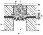
- the ink-jet printhead includes a substrate 30 , a vibration plate 38 , an ink chamber 37 , a passage plate 40 , and a nozzle plate 50 .
- the substrate 30 is perforated from a rear side into a top surface and includes a space portion 32 covered with a base layer 31 formed on the surface of the substrate 30 .
- the substrate 30 is formed of silicon, which is widely used in manufacturing an integrated circuit (IC).
- the vibration plate 38 is installed at a top surface of the substrate 30 and ejects ink by a high pressure of the ink chamber 37 , which is caused by a volume variation of the ink chamber 37 , using a shape memory alloy, of which shape varies according to a temperature variation.
- the vibration plate 36 includes the base layer 31 , a heating element 33 , an electrode 34 , an insulating layer 35 , and a thin film shape memory alloy layer 36 .
- the base layer 31 is formed at the top surface of the substrate 30 to cover the space portion 32 .
- the base layer 31 is formed of silicon oxide, SiOx, by oxidizing the substrate 30 to a thickness between 0.5 ⁇ m and 3 ⁇ m.
- the base layer 31 has a residual compressive stress and is bending-deformed toward the space portion 32 .
- the heating element 33 is installed at a top surface of the base layer 31 and generates heat transferred to the thin film shape memory alloy layer 36 .
- the heating element 33 is formed of one selected from materials, such as TaAl, NiCr, TaN, Ta, Ni, and doped Poly-Si, having resistivity more than 100 ⁇ cm and a temperature coefficient of resistance (TCR) less than ⁇ 1000 ppm.
- the heating element 33 is formed on the base layer 31 through a sputtering, evaporation, or chemical vapor deposition (CVD). According to another aspect of the present invention, a melting point of the heating element 33 is higher than 800° C., and the heating element 33 has a thickness between 0.05 ⁇ m and 0.3 ⁇ m.
- the electrode 34 contacts at least both sides of the heating element 33 and supplies current to the heating element 33 from an external power source.
- the electrode 34 has a resistivity between 10 ⁇ cm and 100 ⁇ cm and a melting point of more than 800° C., and is made of one of Al, Au, Pt, Poly-Si, and WSi 2 .
- a thickness of the electrode 34 is more than 0.2 ⁇ m.
- the insulating layer 35 is formed on a top surface of the heating element 33 and the electrode 34 , transfers heat generated by the heating element 33 to the thin film shape memory alloy layer 36 , and is electrically insulated from the heating element 33 .
- the insulating layer 35 is formed of a passivation layer deposited on the heating element 33 .
- the passivation layer such as SiNx, SiC, diamond like carbon (DLC), and SiOx, has good thermal conductivity, low specific heat, high ink resistance, and excellent mechanical strength, through the CVD or sputtering. It is possible that a thickness of the insulating layer 35 is between 0.05 ⁇ m and 1 ⁇ m.
- the thin film shape memory alloy 36 is formed on a top surface of the insulating layer 35 , and a phase of the thin film shape memory alloy 36 is successively transformed in accordance with the temperature variation, and the thin film shape memory alloy layer 36 changes a volume of the ink chamber 37 during the phase transformation.
- the thin film shape memory alloy layer 36 memories an original state at a predetermined temperature through a thermal treatment (400-700° C.) and is returned from a deformed state to the original state when heat transferred from the heating element 33 reaches the predetermined temperature.
- the thin film shape memory alloy layer 36 is bent toward the space portion 32 in the deformed state during cooling, that is, when heat is not transferred from the heating element 33 .
- the thin film shape memory alloy layer 36 is returned from the deformed state to a flat state as the original state when heat transferred from the heating element 33 reaches the predetermined temperature. And then, the thin film shape memory alloy layer 36 is bent again toward the space portion 32 when cooling. It is possible that the thin film shape memory alloy layer 36 is formed of a combination of Ni, Ti, and Cu to a thickness between 0.5 ⁇ m and 5 ⁇ m.
- the ink chamber 37 is formed on a top surface of the vibration plate 38 and is surrounded by a passage plate 40 to store ink 39 to be ejected.
- the thin film shape memory alloy layer 36 directly contacts the ink 39 , since the heating element 33 is separated from the thin film shape memory alloy layer 36 by the insulating layer 34 , the heating element 33 does not directly contact the ink 39 . Accordingly, there is no concern that the current directly flows to the ink 39 .
- the passage plate 40 is formed of a photosensitive material, such as photoresistive film-vacrel, Su-8, and pymel, laminated on the vibration plate 38 .
- the nozzle plate 50 is installed at a top surface of the passage plate 40 and includes a nozzle 51 to eject the ink 39 contained in a center of the ink chamber 37 onto a printing sheet.
- a diameter of the nozzle 51 is smaller than that of the ink chamber 37 .
- FIGS. 3A through 3C An ink ejection mechanism of the ink-jet printhead having the structure described above will be described with reference to FIGS. 3A through 3C .
- Reference numerals the same as those of FIG. 2 denote elements having the same functions.
- a residual compressive stress exists in the base layer 31 , and thus the base layer 31 is bent toward the space portion 32 causing a buckling phenomenon that the vibration plate 38 , in which the heating element 33 , the insulating layer 35 , and the thin film shape memory alloy 32 are sequentially stacked on the base layer 31 , is bent toward the space portion 32 .
- the ink 39 stored in the ink reservoir flows into the ink chamber 37 through the ink inlet by the capillary action.
- the ink chamber 37 is filled with the ink 39 .
- the heating element 33 when the current flows to the heating element 33 from the external power source through the electrode 34 , the heating element 33 generates heat. A portion of the heat generated from the heating element 33 may be transferred to the space portion 32 or the substrate 30 through the base layer 31 , but most of the heat is transferred to the thin film shape memory alloy layer 36 through the insulating layer 35 .
- the thin film shape memory alloy layer 36 When a temperature of the thin film shape memory alloy layer 36 increases by the transferred heat and reaches the predetermined temperature, the thin film shape memory alloy layer 36 is in the memorized flat state as the original state. Then, the vibration plate 38 overcomes the residual compressive stress of the base layer 31 by a force with which the thin film shape memory alloy layer 36 is returned to the flat state from the deformed state. Thus, the thin film shape memory alloy layer 36 moves in an arrow direction of FIG. 3B to return to the flat state.
- the heating element 33 does not generate the heat, and thus the thin film shape memory alloy layer 36 is cooled down. Then, the vibration plate 38 moves in an arrow direction of FIG. 3C and is bent toward the space portion 32 .
- the ink droplet 39 a is separated from the nozzle 51 and is ejected onto the printing sheet. New ink 39 is supplied into the ink chamber 37 through the ink inlet, and the ink chamber 37 is filled with the new ink 39 .
- the above operation is repeatedly performed, and the ink-jet printhead ejects the ink 39 onto the printing sheet.
- FIGS. 4A through 4K A method of manufacturing the ink-jet printhead having the above structure according to another embodiment of the present invention will be described with reference FIGS. 4A through 4K .
- FIGS. 4A through 4K are cross-sectional views illustrating the method of manufacturing the ink-jet printhead.
- the method of manufacturing the ink-jet printhead is largely categorized into three operations: forming the vibration plate 38 on the substrate 30 as shown in FIGS. 4A through 4F , forming the space portion 32 as shown in FIGS. 4G through 4H , and forming the passage plate 40 and joining the nozzle plate 50 , which is separately manufactured, onto the passage plate 40 as shown in FIGS. 4I through 4K .
- silicon oxide layers 31 , 31 ′ are formed on the surface and the rear side of the substrate 30 .
- a silicon substrate is used for the substrate 30 since a silicon wafer (substrate) is widely used in manufacturing a semiconductor device and can be used to be effective in mass production.
- the silicon oxide layers (SOx) 31 and 31 ′ are formed on the surface and the rear side of the silicon substrate 30 .
- the silicon oxide layer 31 formed on the surface of the substrate 30 is referred to as the base layer 31 of FIGS. 2-3C .
- the heating element 33 is formed on the silicon oxide layer 31 formed on the surface of the substrate 30 .
- the heating element 33 is formed by coating a material having a resistivity more than 100 ⁇ cm and a TCR less than ⁇ 1000 ppm to a thickness between 0.05 ⁇ m and 0.3 ⁇ m through the sputtering, evaporation, or CVD.
- the electrode 34 applying the current to the heating element 33 is formed on the heating element 33 .
- the electrode 34 is formed by coating a conductive material having the resistivity less than several tens of ⁇ cm and a thickness of more than 0.2 ⁇ m through sputtering, evaporation, or CVD.
- the electrode 34 formed on the heating element 33 is patterned and etched through a lithographic process and an etching process, thereby exposing a portion of the heating element 33 .
- a non-etched portion of the electrode 34 contacts the heating element 33 .
- the insulating layer 35 is formed on the electrode 34 and on the heating element 33 .
- the insulating layer 35 prevents the heating element 33 and the thin film shape memory alloy layer 36 from contacting each other by separating the heating element 33 from the thin film shape memory alloy layer 36 .
- the insulating layer 35 is electrically insulated but must transfer heat generated by the heating element 33 to the thin film shape memory alloy layer 36 .
- the insulating layer 35 is formed of the passivation layer, which has a good thermal conductivity, a low specific heat, a high ink resistance, and an excellent mechanical strength, deposited on the heating element 33 through the CVD or sputtering.
- the thin film shape memory alloy layer 36 is thinly deposited on the insulating layer 35 through the sputtering, and the original state of the thin film shape memory alloy layer 36 is memorized through the thermal treatment at a temperature between 400° C. and 700° C.
- the thin film shape memory alloy layer 36 memories the flat state as the original state.
- the thin film shape memory alloy layer 36 is patterned and etched to a size of a desired region through the lithographic process and the etching process.
- an operation of etching a part of the insulating layer 35 and exposing the electrode 34 may be added.
- the exposing of the electrode 34 may be performed after forming the thin film shape memory alloy layer 36 as described above.
- the vibration plate 38 is formed on the substrate 30 .
- the silicon oxide layer 31 ′ formed on the rear side of the substrate 30 is patterned and etched, thereby exposing a part of the substrate 30 .
- the exposed substrate 30 is wet- or dry-etched to a predetermined depth, thereby forming the space portion 32 .
- the base layer 31 covering the space portion 32 is bent toward the space portion 32 by a buckling phenomenon.
- the residual compressive stress exists in the base layer 31 , the residual compressive stress is exerted from both ends of the base layer 31 to a center portion of the base layer 31 , and thus the base layer 31 tends to be bent toward the space portion 32 .
- the heating element 33 , the insulating layer 35 , and the thin film shape memory alloy 36 are sequentially stacked on the base layer 31 , and since a lower portion of the base layer 31 is disturbed by the substrate 30 before the substrate is etched to form the space portion 32 , the base layer 31 is not bent in any direction. In such a case, a portion of the substrate 30 corresponding to the space portion 32 is removed to cause the base layer 31 to be bent toward the space portion 32 by the compressive stress.
- the base layer 31 , the heating element 33 , the insulating layer 35 , and the thin film shape memory alloy layer 36 are joined together in the vibration plate 38 and thus are bent together.
- a photosensitive layer such as film-shaped photoresist
- a photosensitive layer such as liquid-shaped photoresist
- the photosensitive layer is patterned and etched, thereby forming the ink chamber 37 and the passage plate 40 surrounding the ink chamber 37 .
- the thin film shape memory alloy layer 36 is exposed to the ink chamber 37 .
- ink inlet as the path for supplying ink from the ink reservoir to the ink chamber 37 may be performed.
- the nozzle plate 50 which is separately manufactured, is joined onto the passage plate 40 , thereby completing the ink-jet printhead according to the present invention.
- the nozzle 51 is formed at the nozzle plate 50 to eject the ink 39 .
- the nozzle plate 50 is formed through plating, polishing processing, or laser processing.
- materials may be used for materials used in constituting each element of the ink-jet printhead in the present invention, and methods of stacking and forming each material are only illustrated but various deposition and etching methods may be made.
- the order of the operations may be different as the demands.
- the ink-jet printhead according to the present invention has the following advantages. First, a heating efficiency increases due to the high resistivity of the heating element, thereby reducing a power consumption and realizing a power-savings in driving the ink-jet printhead.
- a height and a range of voltages can be easily controlled, and thus a power can be precisely controlled, thereby exactly regulating the amount of the ejected ink and having a predetermined image quality.
- the heating element does not contact directly the ink, thereby realizing stability of the heating element.
- the vibration plate becomes thick, thereby increasing a shockproof property and durability of the ink-jet printhead.
Landscapes
- Engineering & Computer Science (AREA)
- Manufacturing & Machinery (AREA)
- Particle Formation And Scattering Control In Inkjet Printers (AREA)
Abstract
Description
Claims (19)
Priority Applications (1)
| Application Number | Priority Date | Filing Date | Title |
|---|---|---|---|
| US12/000,579 US7758165B2 (en) | 2001-11-29 | 2007-12-13 | Ink-jet printhead and manufacturing method thereof |
Applications Claiming Priority (2)
| Application Number | Priority Date | Filing Date | Title |
|---|---|---|---|
| KR10-2001-0074962A KR100433528B1 (en) | 2001-11-29 | 2001-11-29 | Inkjet printhead and manufacturing method thereof |
| KR2001-74962 | 2001-11-29 |
Related Child Applications (1)
| Application Number | Title | Priority Date | Filing Date |
|---|---|---|---|
| US12/000,579 Division US7758165B2 (en) | 2001-11-29 | 2007-12-13 | Ink-jet printhead and manufacturing method thereof |
Publications (2)
| Publication Number | Publication Date |
|---|---|
| US20030098899A1 US20030098899A1 (en) | 2003-05-29 |
| US7341332B2 true US7341332B2 (en) | 2008-03-11 |
Family
ID=19716439
Family Applications (2)
| Application Number | Title | Priority Date | Filing Date |
|---|---|---|---|
| US10/268,726 Expired - Fee Related US7341332B2 (en) | 2001-11-29 | 2002-10-11 | Ink-jet printhead and manufacturing method thereof |
| US12/000,579 Expired - Fee Related US7758165B2 (en) | 2001-11-29 | 2007-12-13 | Ink-jet printhead and manufacturing method thereof |
Family Applications After (1)
| Application Number | Title | Priority Date | Filing Date |
|---|---|---|---|
| US12/000,579 Expired - Fee Related US7758165B2 (en) | 2001-11-29 | 2007-12-13 | Ink-jet printhead and manufacturing method thereof |
Country Status (2)
| Country | Link |
|---|---|
| US (2) | US7341332B2 (en) |
| KR (1) | KR100433528B1 (en) |
Cited By (1)
| Publication number | Priority date | Publication date | Assignee | Title |
|---|---|---|---|---|
| US9427966B2 (en) * | 2013-03-15 | 2016-08-30 | Konica Minolta, Inc. | Inkjet head, method for manufacturing same, and inkjet printer |
Families Citing this family (10)
| Publication number | Priority date | Publication date | Assignee | Title |
|---|---|---|---|---|
| US7334871B2 (en) * | 2004-03-26 | 2008-02-26 | Hewlett-Packard Development Company, L.P. | Fluid-ejection device and methods of forming same |
| TW200600348A (en) * | 2004-06-17 | 2006-01-01 | Ind Tech Res Inst | Inkjet printhead |
| US7913928B2 (en) * | 2005-11-04 | 2011-03-29 | Alliant Techsystems Inc. | Adaptive structures, systems incorporating same and related methods |
| KR101206812B1 (en) * | 2007-07-02 | 2012-11-30 | 삼성전자주식회사 | Inkjet printhead and method of manufacturing thereof |
| KR200454116Y1 (en) * | 2008-11-17 | 2011-06-16 | 주식회사 혼 | Display rack variable expandable showcase |
| US9211703B2 (en) * | 2012-12-13 | 2015-12-15 | Palo Alto Research Center Incorporated | Temperature dependent shape elements for void control in ink jet printers |
| US10038267B2 (en) * | 2014-06-12 | 2018-07-31 | Palo Alto Research Center Incorporated | Circuit interconnect system and method |
| KR101600895B1 (en) * | 2014-09-04 | 2016-03-09 | 쌍용전기 주식회사 | Bushing for Transformer |
| US10363731B2 (en) * | 2014-12-18 | 2019-07-30 | Palo Alto Research Center Incorporated | Ejector device |
| CN105107670A (en) * | 2015-09-17 | 2015-12-02 | 厦门理工学院 | Driving type liquid micro-jet method and device for memory metal |
Citations (11)
| Publication number | Priority date | Publication date | Assignee | Title |
|---|---|---|---|---|
| US5719604A (en) * | 1994-09-27 | 1998-02-17 | Sharp Kabushiki Kaisha | Diaphragm type ink jet head having a high degree of integration and a high ink discharge efficiency |
| US5883650A (en) * | 1995-12-06 | 1999-03-16 | Hewlett-Packard Company | Thin-film printhead device for an ink-jet printer |
| US5956058A (en) * | 1993-11-05 | 1999-09-21 | Seiko Epson Corporation | Ink jet print head with improved spacer made from silicon single-crystal substrate |
| US5988799A (en) * | 1995-09-25 | 1999-11-23 | Sharp Kabushiki Kaisha | Ink-jet head having ink chamber and non-ink chamber divided by structural element subjected to freckling deformation |
| JP2000141635A (en) | 1998-11-04 | 2000-05-23 | Minolta Co Ltd | Ink jet head |
| US6123414A (en) * | 1997-03-12 | 2000-09-26 | Samsung Electro-Mechanics Co., Ltd. | Apparatus for injecting a recording solution of a print head using phase transformation of thin film shape memory alloy |
| US6126272A (en) * | 1997-01-15 | 2000-10-03 | Samsung Electronics Co., Ltd. | Ink spraying device for print head |
| US6130689A (en) * | 1997-11-19 | 2000-10-10 | Samsung Electro-Mechanics Co., Ltd. | Apparatus and actuator for injecting a recording solution of a print head and method for producing the apparatus |
| US6354698B1 (en) * | 1997-12-26 | 2002-03-12 | Canon Kabushiki Kaisha | Liquid ejection method |
| US6527813B1 (en) * | 1996-08-22 | 2003-03-04 | Canon Kabushiki Kaisha | Ink jet head substrate, an ink jet head, an ink jet apparatus, and a method for manufacturing an ink jet recording head |
| US6652969B1 (en) * | 1999-06-18 | 2003-11-25 | Nissin Electric Co., Ltd | Carbon film method for formation thereof and article covered with carbon film and method for preparation thereof |
Family Cites Families (3)
| Publication number | Priority date | Publication date | Assignee | Title |
|---|---|---|---|---|
| JPH10173306A (en) * | 1996-12-06 | 1998-06-26 | Olympus Optical Co Ltd | Manufacturing method of shape memory alloy thin-film actuator |
| US6766817B2 (en) * | 2001-07-25 | 2004-07-27 | Tubarc Technologies, Llc | Fluid conduction utilizing a reversible unsaturated siphon with tubarc porosity action |
| US7285255B2 (en) * | 2002-12-10 | 2007-10-23 | Ecolab Inc. | Deodorizing and sanitizing employing a wicking device |
-
2001
- 2001-11-29 KR KR10-2001-0074962A patent/KR100433528B1/en not_active Expired - Fee Related
-
2002
- 2002-10-11 US US10/268,726 patent/US7341332B2/en not_active Expired - Fee Related
-
2007
- 2007-12-13 US US12/000,579 patent/US7758165B2/en not_active Expired - Fee Related
Patent Citations (11)
| Publication number | Priority date | Publication date | Assignee | Title |
|---|---|---|---|---|
| US5956058A (en) * | 1993-11-05 | 1999-09-21 | Seiko Epson Corporation | Ink jet print head with improved spacer made from silicon single-crystal substrate |
| US5719604A (en) * | 1994-09-27 | 1998-02-17 | Sharp Kabushiki Kaisha | Diaphragm type ink jet head having a high degree of integration and a high ink discharge efficiency |
| US5988799A (en) * | 1995-09-25 | 1999-11-23 | Sharp Kabushiki Kaisha | Ink-jet head having ink chamber and non-ink chamber divided by structural element subjected to freckling deformation |
| US5883650A (en) * | 1995-12-06 | 1999-03-16 | Hewlett-Packard Company | Thin-film printhead device for an ink-jet printer |
| US6527813B1 (en) * | 1996-08-22 | 2003-03-04 | Canon Kabushiki Kaisha | Ink jet head substrate, an ink jet head, an ink jet apparatus, and a method for manufacturing an ink jet recording head |
| US6126272A (en) * | 1997-01-15 | 2000-10-03 | Samsung Electronics Co., Ltd. | Ink spraying device for print head |
| US6123414A (en) * | 1997-03-12 | 2000-09-26 | Samsung Electro-Mechanics Co., Ltd. | Apparatus for injecting a recording solution of a print head using phase transformation of thin film shape memory alloy |
| US6130689A (en) * | 1997-11-19 | 2000-10-10 | Samsung Electro-Mechanics Co., Ltd. | Apparatus and actuator for injecting a recording solution of a print head and method for producing the apparatus |
| US6354698B1 (en) * | 1997-12-26 | 2002-03-12 | Canon Kabushiki Kaisha | Liquid ejection method |
| JP2000141635A (en) | 1998-11-04 | 2000-05-23 | Minolta Co Ltd | Ink jet head |
| US6652969B1 (en) * | 1999-06-18 | 2003-11-25 | Nissin Electric Co., Ltd | Carbon film method for formation thereof and article covered with carbon film and method for preparation thereof |
Cited By (1)
| Publication number | Priority date | Publication date | Assignee | Title |
|---|---|---|---|---|
| US9427966B2 (en) * | 2013-03-15 | 2016-08-30 | Konica Minolta, Inc. | Inkjet head, method for manufacturing same, and inkjet printer |
Also Published As
| Publication number | Publication date |
|---|---|
| KR20030044264A (en) | 2003-06-09 |
| US7758165B2 (en) | 2010-07-20 |
| US20030098899A1 (en) | 2003-05-29 |
| US20080096296A1 (en) | 2008-04-24 |
| KR100433528B1 (en) | 2004-06-02 |
Similar Documents
| Publication | Publication Date | Title |
|---|---|---|
| US7758165B2 (en) | Ink-jet printhead and manufacturing method thereof | |
| JP3642756B2 (en) | Fluid jet print head and method of manufacturing fluid jet print head | |
| JP2000198205A (en) | Fluid ejection device and method of manufacturing the same | |
| US7036913B2 (en) | Ink-jet printhead | |
| US8100511B2 (en) | Heater of an inkjet printhead and method of manufacturing the heater | |
| US20090058952A1 (en) | Inkjet printhead and method of manufacturing the same | |
| US20080213927A1 (en) | Method for manufacturing an improved resistive structure | |
| EP1442887B1 (en) | Droplet ejector and ink-jet printhead using the same | |
| US20060044347A1 (en) | Inkjet printer head and method of fabricating the same | |
| US6322202B1 (en) | Heating apparatus for micro injecting device and method for fabricating the same | |
| US6979076B2 (en) | Ink-jet printhead | |
| US20050134643A1 (en) | Ink-jet printhead and method of manufacturing the same | |
| US7506442B2 (en) | Method of fabricating inkjet printhead | |
| US7018019B2 (en) | Ink-jet printhead and method for manufacturing the same | |
| KR100337112B1 (en) | Printer head | |
| US20070070127A1 (en) | Inkjet printhead and method of manufacturing the same | |
| KR100513717B1 (en) | Bubble-jet type inkjet printhead | |
| KR20050014130A (en) | Ink-jet printhead driven piezoelectrically and electrostatically and method for manufacturing method thereof | |
| KR100421027B1 (en) | Inkjet printhead and manufacturing method thereof | |
| JPH0592567A (en) | Liquid jet recording apparatus and method, and recording head manufacturing method thereof | |
| KR20040079634A (en) | Inkjet printhead and method of manufacturing thereof | |
| KR19990041107A (en) | Printhead and its manufacturing method | |
| JP2000301712A (en) | Ink jet recording head |
Legal Events
| Date | Code | Title | Description |
|---|---|---|---|
| AS | Assignment |
Owner name: SAMSUNG ELECTRONICS CO., LTD., KOREA, REPUBLIC OF Free format text: ASSIGNMENT OF ASSIGNORS INTEREST;ASSIGNORS:JUNG, MYUNG-SONG;PARK, SUNG-JOON;KIM, TAE-KYUN;AND OTHERS;REEL/FRAME:013379/0264 Effective date: 20021002 Owner name: ARUZE CO., LTD., JAPAN Free format text: ASSIGNMENT OF ASSIGNORS INTEREST;ASSIGNOR:OKADA, KAZUO;REEL/FRAME:013379/0468 Effective date: 20021010 |
|
| FEPP | Fee payment procedure |
Free format text: PAYOR NUMBER ASSIGNED (ORIGINAL EVENT CODE: ASPN); ENTITY STATUS OF PATENT OWNER: LARGE ENTITY |
|
| CC | Certificate of correction | ||
| FEPP | Fee payment procedure |
Free format text: PAYER NUMBER DE-ASSIGNED (ORIGINAL EVENT CODE: RMPN); ENTITY STATUS OF PATENT OWNER: LARGE ENTITY Free format text: PAYOR NUMBER ASSIGNED (ORIGINAL EVENT CODE: ASPN); ENTITY STATUS OF PATENT OWNER: LARGE ENTITY |
|
| FPAY | Fee payment |
Year of fee payment: 4 |
|
| REMI | Maintenance fee reminder mailed | ||
| LAPS | Lapse for failure to pay maintenance fees | ||
| STCH | Information on status: patent discontinuation |
Free format text: PATENT EXPIRED DUE TO NONPAYMENT OF MAINTENANCE FEES UNDER 37 CFR 1.362 |
|
| STCH | Information on status: patent discontinuation |
Free format text: PATENT EXPIRED DUE TO NONPAYMENT OF MAINTENANCE FEES UNDER 37 CFR 1.362 |
|
| FP | Lapsed due to failure to pay maintenance fee |
Effective date: 20160311 |
|
| AS | Assignment |
Owner name: S-PRINTING SOLUTION CO., LTD., KOREA, REPUBLIC OF Free format text: ASSIGNMENT OF ASSIGNORS INTEREST;ASSIGNOR:SAMSUNG ELECTRONICS CO., LTD;REEL/FRAME:041852/0125 Effective date: 20161104 |