US7327378B2 - Laser scanning unit - Google Patents
Laser scanning unit Download PDFInfo
- Publication number
- US7327378B2 US7327378B2 US10/750,894 US75089404A US7327378B2 US 7327378 B2 US7327378 B2 US 7327378B2 US 75089404 A US75089404 A US 75089404A US 7327378 B2 US7327378 B2 US 7327378B2
- Authority
- US
- United States
- Prior art keywords
- motor
- scanning unit
- laser scanning
- inverter
- section
- Prior art date
- Legal status (The legal status is an assumption and is not a legal conclusion. Google has not performed a legal analysis and makes no representation as to the accuracy of the status listed.)
- Expired - Lifetime, expires
Links
Images


Classifications
-
- G—PHYSICS
- G02—OPTICS
- G02B—OPTICAL ELEMENTS, SYSTEMS OR APPARATUS
- G02B26/00—Optical devices or arrangements for the control of light using movable or deformable optical elements
- G02B26/08—Optical devices or arrangements for the control of light using movable or deformable optical elements for controlling the direction of light
- G02B26/10—Scanning systems
- G02B26/12—Scanning systems using multifaceted mirrors
- G02B26/121—Mechanical drive devices for polygonal mirrors
- G02B26/122—Control of the scanning speed of the polygonal mirror
-
- H—ELECTRICITY
- H02—GENERATION; CONVERSION OR DISTRIBUTION OF ELECTRIC POWER
- H02P—CONTROL OR REGULATION OF ELECTRIC MOTORS, ELECTRIC GENERATORS OR DYNAMO-ELECTRIC CONVERTERS; CONTROLLING TRANSFORMERS, REACTORS OR CHOKE COILS
- H02P6/00—Arrangements for controlling synchronous motors or other dynamo-electric motors using electronic commutation dependent on the rotor position; Electronic commutators therefor
- H02P6/14—Electronic commutators
- H02P6/16—Circuit arrangements for detecting position
- H02P6/18—Circuit arrangements for detecting position without separate position detecting elements
- H02P6/182—Circuit arrangements for detecting position without separate position detecting elements using back-emf in windings
Definitions
- the present invention relates to a laser scanning unit for an image forming and/or reproducing apparatus, and more particularly, to a laser scanning unit in which a motor drive chip for a polygonal mirror motor is installed outside of a housing.
- Laser scanning units are employed in a printing machines such as, for example, laser printers.
- a conventional laser scanning unit includes: a laser source; a movable mirror; and a lens system.
- the laser source emits laser beams which are directed by the mirror and the lens system to a surface of a charged photoconductive medium, such as a photoconductive drum or a photoconductive belt.
- the lens system compensates for any image distortion caused by, for example, the varying distance between the mirror and points along the photosensitive drum or belt.
- the laser beam changes the charge of portions of the photoconductive medium on which it is incident forming a latent image on the photoconductive medium which corresponds to the image to be printed and to which toner may adhere.
- FIG. 1 is an exploded view illustrating the internal configuration of a conventional laser scanning unit.
- the conventional laser scanning unit includes various optical elements.
- the optical elements include a laser diode (LD) 11 emitting a laser beam, a collimating lens 12 collimating a laser beam emitted from the LD 11 so that the laser beam is parallel to or lined up with an optical axis, a polygonal mirror 14 horizontally moving a laser beam which has passed through the collimating lens 12 at a constant linear speed, a cylindrical lens 13 imaging a laser beam on a surface of the polygonal mirror 14 in a horizontally linear shape, F ⁇ lenses 15 having a refractive index with respect to the optical axis which lenses polarize a laser beam reflected by the polygonal mirror 14 at a constant speed to a main scanning direction and correcting aberration to focus the laser beam on a scanned surface, an image-forming mirror 16 reflecting a laser beam which has passed through the F ⁇ lenses 15 and imaging the laser beam in the form of dots on a surface of a photoconductive drum 60 of a printing machine, an optical sensor 18
- a motor 20 rotating the polygonal mirror 14 at a constant speed is installed on a circuit board 30 within the housing 50 .
- a motor drive chip 40 formed of a semiconductor integrated circuit is mounted on the circuit board 30 to drive and control the motor 20 .
- a circuit board 10 controlling the LD 11 is disposed inside the housing 50 .
- FIG. 2 is a block diagram illustrating the circuit configuration of the motor drive chip of the conventional laser scanning unit of FIG. 1 .
- the motor 20 rotating the polygonal mirror 14 at a constant speed includes three position sensors 21 , 22 , and 23 , and a speed sensor 24 .
- hall sensors are used as the sensors 21 , 22 , 23 , and 24 .
- the motor drive chip 40 includes a position signal amplifying section 41 , a speed signal amplifying and filtering section 42 , a speed control section 43 , a commutation control section 44 , and a three-phase inverter 45 .
- the sensors 21 , 22 , and 23 are each connected to the position signal amplifying section 41 of the motor drive chip 40 by two signal lines.
- the speed sensor 24 is connected to the speed signal amplifying and filtering section 42 by two signal lines.
- the three-phase inverter 45 is respectively connected to terminals u, v, and w of the motor 20 (shown in FIG. 1 ) by three power supply lines.
- the position signal amplifying section 41 amplifies position signals Sa, Sb, and Sc of a rotor of the motor 20 (shown in FIG. 1 ) respectively received from the position sensors 21 , 22 and 23 and transmits the amplified signals to the commutation control section 44 .
- the speed signal amplifying and filtering section 42 amplifies and filters a speed signal Sd received from the speed sensor 24 and transmits the amplified and filtered signal to the speed control section 43 .
- the speed control section 43 calculates a control signal to control the rotation speed of the motor 20 in response to the received speed signal and transmits the control signal to the commutation control section 44 .
- the commutation control section 44 controls the three-phase inverter 45 in response to the received position signal and the speed control signal.
- the inverter 45 respectively supplies current in a proper switching order to the terminals u, v, and w of the motor 20 so that the motor 20 rotates at a constant speed.
- the motor drive chip 40 is disposed inside the housing 50 . Further, the motor drive chip 40 acts as a heat-source during operation. As a result, during operation, the temperature inside the laser scanning unit increases due to heat generated by the motor drive chip 40 . Properties of the LD 11 and the F ⁇ lens 15 are temperature sensitive. Consequently, the temperature increase inside the laser scanning unit affects properties of the LD 11 and the F ⁇ lens 15 .
- Tables 1 and 2 present measurement results of internal temperature changes and temperature changes in each element in the conventional laser scanning unit.
- Table 1 shows temperature changes (in ° C.) in each element of the laser scanning unit over time when a motor is continuously driven at 22,000 rpm under low temperature/humidity conditions.
- Table 2 shows temperature changes (in ° C.) in each element in the laser scanning unit over time when a motor is continuously driven at 22,000 rpm under high temperature/humidity conditions.
- the internal temperature increase in the laser scanning unit is slightly affected by the environment in which the laser scanning unit is used as well as conditions of use of the laser scanning unit.
- the temperature of each element of the laser scanning unit also increases.
- the degree of temperature increase in each element increases.
- the surface temperature of the motor drive chip exhibits the largest increase
- the surface temperature of the polygonal mirror motor exhibits the second largest increase. Therefore, it is shown that the greatest cause of the internal temperature increase of the laser scanning unit is the motor drive chip.
- the internal temperature increase of the laser scanning unit due to heat generated by the motor drive chip leads to the temperature increase of the laser diode. Consequently, the temperature characteristic of the laser diode changes and, as a result, the optical power of the laser diode cannot be controlled with precision.
- the internal temperature increase of the laser scanning unit causes the temperature of the F ⁇ lens to increase.
- the temperature increase of the F ⁇ lens which is typically injection molded plastic, affects the refractive index and curvature of each region in the F ⁇ lens. As a result, variation of the diameter of the optical spot formed on a surface of the photoconductive medium increases.
- Table 3 presents measurement results of diameters of an optical spot with changes in the temperature inside the laser scanning unit.
- Positions of the optical spot that is, 0, ⁇ 100, and 100 mm, represent the center of a scanning line and distances from the center to both ends of the scanning line, respectively, and ⁇ 2 mm ⁇ +2 mm represents changes in the length of the F ⁇ lens with temperature changes.
- “Main” and “sub” represent diameters of a main scanning direction and a sub scanning direction of the optical spot, respectively.
- One approach to addressing the above-described disadvantages is to dispose the motor drive chip 40 outside of the housing 50 so that the motor drive chip 40 is isolated from the LD 11 and the F ⁇ lenses 15 .
- locating the motor drive chip 40 outside of the housing exposes the signal and power supply lines to outside interference.
- a plurality of signal lines which respectively connect the motor drive chip 40 to the sensors 21 , 22 , 23 , and 24 included in the motor 20 and the power supply lines which supply electric power to the motor 20 are exposed outside the housing 50 .
- severe noise is generated due to an] by electromagnetic fields outside the housing 50 .
- the position and speed sensors are typically low voltage sensors such as, for example, hall sensors which output sine wave signals of approximately ⁇ 0.1 ⁇ 0.2V. Since the sensor output voltage is low, the output signals are very sensitive to noise, and accordingly, in the conventional art, the motor drive chip 40 needs to be positioned as close as possible to the position and speed sensors 21 , 22 , 23 , and 24 .
- the present invention provides a laser scanning unit in which a motor drive chip for a polygonal mirror motor is disposed outside of a housing to eliminate the effects of increased temperature caused by the motor drive chip so as to obtain a stable optical power from a laser diode, and a motor is controlled using a sensorless control algorithm to minimize noise.
- a laser scanning unit including: a housing; an optical system disposed in the housing and including an optical source which emits a laser beam, a mirror which scans the laser beam, and a plurality of optical elements which image the laser beam on an image surface; a motor disposed in the housing and which rotates the mirror; and a motor drive chip disposed outside of the housing and which controls a rotation speed of the motor.
- the motor drive chip may be mounted on a main printed circuit board of a printing machine with which the laser scanning unit is used.
- the motor drive chip may be electrically connected to the motor by a cable, and the cable may be a flexible printed circuit board.
- the motor drive chip may control the motor via a sensorless control algorithm using back-electromotive forces generated by the motor, and the motor drive chip and the motor may be connected by power supply and back-electromotive signal lines.
- the motor drive chip may include: a motor starting section which generates a motor starting signal to start the motor; an inverter which applies current to the motor in response to the motor starting signal; a back-electromotive force detecting section which detects back-electromotive forces generated rotation of the motor; a speed control section which detects the position of a rotor of the motor and the speed of the motor based on waveforms of the back-electromotive forces detected by the back-electromotive force detecting section to generate a speed control signal; and a commutation control section which controls the inverter in response to the speed control signal.
- the motor drive chip may rotate the motor at a constant speed via a sensorless control algorithm using current supplied to the motor, the inductance of the motor, a third harmonic voltage of a stator of the motor, or electromagnetic flux generated between the stator and the rotor of the motor.
- a laser scanning unit including: a housing; an optical source which emits a laser beam; a mirror which scans the laser beam; a plurality of optical elements which image the laser beam onto an image surface; a motor which rotates the mirror; and a motor drive chip which controls a rotation speed of the motor.
- the optical source, the mirror, the plurality of optical elements, and the motor are disposed in the housing, and the motor drive chip is disposed outside of the housing.
- a laser scanning unit including: an optical system disposed in an enclosure and including an optical source which emits a laser beam, a mirror which scans the laser beam, and a plurality of optical elements which image the laser beam onto an image surface; a motor disposed in the enclosure and which rotates the mirror; and a motor drive chip disposed outside of the enclosure and which controls a rotation speed of the motor.
- a laser scanning unit including: an enclosure enclosing an optical source which emits a laser beam, a mirror which scans the laser beam, a plurality of optical elements which image the laser beam on an image surface, and a motor disposed in the enclosure and which rotates the polygonal mirror; and a motor drive chip disposed outside of the enclosure and which controls a rotation speed of the motor.
- a method of improving imaging resolution and uniformity of a laser scanning unit includes: enclosing an optical source which emits a laser beam, a mirror which scans the laser beam, a plurality of optical elements which image the laser beam on an image surface, and a motor and which rotates the mirror; and controlling the motor via a motor drive chip disposed outside of the enclosure using a sensorless control algorithm.
- a method of moderating a temperature characteristic of a laser diode including: enclosing an optical source which emits a laser beam, a mirror which scans the laser beam, a plurality of optical elements which image the laser beam on an image surface, and a motor and which rotates the mirror; and controlling the motor via a motor drive chip disposed outside of the enclosure using a sensorless control algorithm.
- FIG. 1 is a perspective view illustrating an internal configuration of a conventional laser scanning unit
- FIG. 2 is a block diagram illustrating a circuit configuration of a motor drive chip of the conventional laser scanning unit of FIG. 1 ;
- FIG. 3 is a perspective view illustrating the overall configuration of a laser scanning unit according to a first embodiment of the present invention
- FIG. 4 is a diagram of a block diagram illustrating a circuit configuration of a motor driven by a motor drive chip according to the first embodiment of the present invention.
- FIG. 5 is a diagram illustrating waveforms of back-electromotive forces detected by a back-electromotive force detection circuit of the motor drive chip of FIG. 4 ;
- FIG. 6 is a block diagram illustrating a circuit configuration of a motor drive chip to drive a motor via a sensorless control algorithm using current supplied to the motor according to a second embodiment of the present invention
- FIG. 7 is a block diagram illustrating a circuit configuration of a motor drive chip to drive a motor via a sensorless control algorithm using the inductance of the motor according to a third embodiment of the present invention
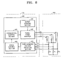
- FIG. 8 is a block diagram illustrating a circuit configuration of a motor drive chip to drive a motor via a sensorless control algorithm using a third harmonic voltage of a stator of the motor according to a fourth embodiment of the present invention.
- FIG. 9 is a block diagram illustrating a circuit configuration of a motor drive chip to drive a motor via a sensorless control algorithm using an electromagnetic flux according to a fifth embodiment of the present invention.
- FIG. 3 is a perspective view illustrating the overall configuration of a laser scanning unit according to an embodiment of the present invention.
- the laser scanning unit includes a housing 150 having a internal space, and an optical system disposed inside the housing 150 and including a plurality of optical elements.
- the housing 150 supports the optical elements of the optical system and encloses the optical elements so that contamination of the optical elements by foreign substances, such as dust particles or toner, is prevented. To this end, the housing is sealable.
- the optical system includes an optical source emitting a laser beam, a mirror 114 scanning the laser beam, and a plurality of optical elements, such as lenses and mirrors, which image the laser beam on an image surface. While a polygonal mirror is described herein, it is to be understood that other configurations are possible.
- a laser diode 111 may be used. However, it is to be understood that while a laser diode is illustrated in FIG. 3 and described hereafter, other optical sources may be used.
- the laser diode 111 is controlled by an optical source control circuit (not shown) mounted on a circuit board 110 .
- a collimating lens 112 and a cylindrical lens 113 are disposed along the optical path of the laser beam emitted from the laser diode 111 .
- the collimating lens 112 collimates a laser beam emitted from the laser diode 111 so that the laser beam is parallel to or convergent on an optical axis, and the cylindrical lens 113 projects the laser beam on a surface of the polygonal mirror 114 in a horizontally linear shape.
- the polygonal mirror 114 horizontally moves a laser beam that has passed through the collimating lens 112 and the cylindrical lens 113 horizontally at a constant linear speed.
- F ⁇ lenses 115 are disposed in front of the polygonal mirror 114 along the optical path of the laser beam after the polygonal mirror 114 .
- the F ⁇ lenses 115 have a refractive index with respect to the optical axis so as to polarize a beam of a constant speed reflected by the polygonal mirror 114 in a main scanning direction and to correct any aberration to focus the beam on an imaging surface.
- a laser beam having passed through the F ⁇ lenses 115 is reflected by an image-forming mirror 116 disposed along the optical path of the laser beam after the F ⁇ lenses 115 so as to be imaged in form of dots on a surface of a photoconductive medium such as, for example, a photoconductive drum 160 , which is an image surface of a printing machine.
- a photoconductive drum is illustrated in FIG. 3 and described hereafter, other photoconductive media may be used.
- a synchronization signal detecting mirror 117 and an optical sensor 118 are interposed between the F ⁇ lenses 115 and the image-forming mirror 116 to receive at least a portion of a laser beam and provide horizontal synchronization.
- the laser scanning unit includes a motor 120 rotating the polygonal mirror 114 and a motor drive chip 140 driving the motor 120 to rotate the motor at a constant speed.
- motor 120 may serve as the motor 120 including, for example, a three-phase brushless DC (BLDC) motor.
- the motor 120 is mounted inside the housing 150 . Since a separate circuit board does not need to be used for the motor 120 , which will be explained in detail below, the motor 120 is directly mountable to the housing 150 .
- BLDC brushless DC
- the motor drive chip 140 is formed of a semiconductor integrated circuit including a plurality of circuits driving and controlling the motor 120 .
- the motor 120 is disposed inside the housing 150 while the motor drive chip 140 is disposed outside the housing 150 .
- the motor drive chip 140 is mountable on a main printed circuit board 170 of the printing machine with which the laser scanning unit according to the first embodiment of the present invention is used.
- the motor drive chip 140 is mountable in other manners.
- the motor drive chip 140 When the motor drive chip 140 is mounted to the main circuit board 170 , the motor drive chip 140 is electrically connectable to the motor 120 via a cable such as, by way of a non-limiting example, a flexible printed circuit board (FPCB) 130 as shown in FIG. 3 .
- a cable such as, by way of a non-limiting example, a flexible printed circuit board (FPCB) 130 as shown in FIG. 3 .
- FPCB flexible printed circuit board
- the motor drive chip 140 since the motor drive chip 140 is disposed outside the housing 150 , the effect of an increase in temperature inside the housing 150 due to heat generated by the motor drive chip 140 is eliminated, and accordingly a stable optical power is obtainable from the laser diode 111 .
- An increase in the temperature of the F ⁇ lenses 115 due to heat generated by the motor drive chip 140 is also prevented, such that the diameter of the optical spot formed on the surface of the photoconductive drum 160 and the diameter variation decrease, thereby improving the resolution and uniformity of an image.
- the motor drive chip 140 when the motor drive chip 140 is outside of the housing, in order to reduce noise due to external electronic waves, the number of signal lines connecting the motor drive chip 140 to the motor 120 is minimized.
- the motor drive chip 140 drives the motor 120 so as to rotate it at a constant speed using a sensorless control algorithm.
- the sensorless control algorithm the motor 120 does not need to be provided with a conventional position sensor and a speed sensor. As a result, signal lines connecting the sensors to the motor drive chip 140 are not required.
- the number of signal lines connecting the motor 120 disposed inside the housing 150 to the motor drive chip 140 disposed outside the housing 150 is reduced, thereby minimizing noise.
- the laser scanning unit according to the first embodiment of the present invention does not employ a position sensor and a speed sensor, such that a separate circuit board for the motor 120 is not required, thereby reducing the manufacturing costs.
- FIG. 4 is a block diagram illustrating a circuit configuration of a motor drive chip for explaining a sensorless control algorithm using back-electromotive forces generated by a motor controlled by a motor drive chip according to the first embodiment of the present invention.
- FIG. 5 is a diagram illustrating waveforms of back-electromotive forces detected by a back-electromotive force detection circuit of the motor drive chip of FIG. 4 .
- the motor drive chip 140 mounted on the main printed circuit board 170 of the printing machine includes a motor starting section 141 , a three-phase inverter 142 , a back-electromotive force detecting section 143 , a speed control section 144 , and a commutation control section 145 .
- the three-phase inverter 142 is respectively connected to terminals u, v, and w of the motor 120 by three power supply lines L 1 , L 2 , and L 3 , respectively.
- the back-electromotive force detecting section 143 is connected to the motor 120 by one back-electromotive force signal line L 4 .
- the motor starting section 141 generates a motor starting signal to start the motor 120 , and the inverter 142 applies current to the motor 120 in response to the motor starting signal to start the motor 120 .
- the generated back-electromotive forces are detected by the back-electromotive force detecting section 143 .
- waveforms of back-electromotive forces Pu, Pv, and Pw in respective phases u, v, and w detected by the back-electromotive force detecting section 143 have a phase difference of 120° therebetween.
- the speed control section 144 respectively senses zero-crossing points of the waveforms of the back-electromotive forces Pu, Pv, and Pw to identify the position of a rotor of the motor 120 , and determines the rotation speed of the motor 120 based on amplitude and time intervals between respective phases to output an appropriate speed control signal.
- the output speed control signal is transmitted to the commutation control section 145 .
- the commutation control section 145 controls the inverter 145 in response to the received speed control signal.
- the inverter 145 accordingly supplies current in a proper switching order to the terminals u, v, and w, respectively, of the motor 120 to rotate the rotor of the motor 120 at a constant speed.
- the motor drive chip 140 is connected to the motor 120 installed inside the housing 150 by the three power supply lines L 1 , L 2 , and L 3 and the back-electromotive force signal line L 4 . Therefore, the number of signal lines is reduced as compared with the conventional art, thereby minimizing noise generated by external electromagnetic waves.
- FIG. 6 is a block diagram illustrating a circuit configuration of a motor drive chip to drive a motor via a sensorless control algorithm using current supplied to the motor according to a second embodiment of the present invention.
- a motor drive chip 240 mounted on a main printed circuit board 170 of a printing machine includes a motor starting section 241 , a three-phase inverter 242 , a current detecting section 243 , a speed control section 244 , and a commutation control section 245 .
- the motor starting section 241 generates a motor starting signal to start the motor 120 .
- the three-phase inverter 242 applies current to the motor 120 according to the motor starting signal to start the motor 120 .
- the current detecting section 243 detects current flowing through three power supply lines L 1 , L 2 , and L 3 respectively connected between terminals u, v, and w of the motor 120 and the three-phase inverter 242 using a current sensor or shunt resistance. Since waveforms of the current respectively supplied to the terminals u, v, and w of the motor 120 are obtainable using two current signals, the current detecting section 243 is respectively connected to the two power supply lines L 1 and L 2 by two current signal lines I 1 and I 2 . However, while I 1 and I 2 are shown as being connected to L 1 and L 2 , I 1 and I 2 need only be connected to any two of L 1 , L 2 , and L 3 .
- Current signals detected by the current detecting section 243 are sine wave signals. Accordingly, the speed control portion 244 identifies the position of the rotor of the motor 120 in the same manner as in the previous embodiment using the back-electromotive forces (i.e., sensing zero-crossing points of waveforms of the current signals), and thus outputs an appropriate speed control signal.
- the commutation control section 245 controls the three-phase inverter 242 according to the received speed control signal.
- the three-phase inverter 242 accordingly supplies current to the terminals u, v, and w of the motor 120 , respectively, in a proper switching order so that the motor 120 rotates at a constant speed.
- FIG. 7 is a block diagram illustrating a circuit configuration of a motor drive chip to drive a motor via a sensorless control algorithm using the inductance of the motor according to a third embodiment of the present invention.
- a motor drive chip 340 mounted on a main printed circuit board 170 of a printing machine includes a motor starting section 341 , a three-phase inverter 342 , an inductance calculating section 343 , a speed control section 344 , and a commutation control section 345 .
- the inductance calculating section 343 detects current and voltage flowing through three power supply lines L 1 , L 2 , and L 3 respectively connected between terminals u, v, and w of the motor 120 and the three-phase inverter 342 .
- the inductance calculating section 343 is respectively connected to the two power supply lines L 1 and L 2 by two current and voltage signal lines P 1 and P 2 .
- P 1 and P 2 are shown as being connected to L 1 and L 2 , P 1 and P 2 need only be connected to any two of L 1 , L 2 , and L 3 .
- Inductance L( ⁇ ) which is a function of the position ⁇ of magnetic flux, is calculable using the current and voltage detected by the inductance calculating section 343 .
- the speed control section 344 detects the position of the rotor of the motor 120 from waveforms of the obtained inductance, and thus outputs an appropriate speed control signal.
- FIG. 8 is a block diagram illustrating a circuit configuration of a motor drive chip to drive a motor via a sensorless control algorithm using a third harmonic voltage of the motor according to a fourth embodiment of the present invention.
- a motor drive chip 440 mounted on a main printed circuit board 170 of a printing machine includes a motor starting section 441 , a three-phase inverter 442 , a third harmonic voltage detecting section 443 , a speed control section 444 and a commutation control section 445 .
- the third harmonic voltage detecting section 443 detects voltage applied to three power supply lines L 1 , L 2 , and L 3 respectively connected between terminals u, v, and w of the motor 120 and the three-phase inverter 442 . For this detection, the third harmonic voltage detecting section 443 is respectively connected to the three power supply lines L 1 , L 2 , and L 3 by three voltage signal lines V 1 , V 2 , and V 3 .
- a third harmonic voltage of the stator of the motor 120 While the motor 120 is rotating, a third harmonic voltage of the stator of the motor 120 has a position component.
- the third harmonic voltage detecting section 443 detects a voltage of the stator in the motor 120 of a Y-connection and sums up all the voltages. The sum of the voltages has a third harmonic voltage component.
- the speed control section 444 recognizes the position of the rotor of the motor 120 using waveforms of the third harmonic voltage with the position component, and thus outputs an appropriate speed control signal.
- FIG. 9 is a block diagram illustrating a circuit configuration of a motor drive chip to drive a motor via a sensorless control algorithm using an electromagnetic flux according to a fifth embodiment of the present invention.
- a motor drive chip 540 mounted on a main printed circuit board 170 of a printing machine includes a motor starting section 541 , a three-phase inverter 542 , an electromagnetic flux calculating section 543 , a speed control section 544 , and a commutation control section 545 .
- the electromagnetic flux calculating section 543 detects current and voltage flowing through three power supply lines L 1 , L 2 , and L 3 respectively connected between terminals u, v, and w of the motor 120 and the three-phase inverter 542 .
- the electromagnetic flux calculating section 543 is respectively connected to the two power supply lines L 1 and L 2 by two current and voltage signal lines P 1 and P 2 .
- P 1 and P 2 are shown as being connected to L 1 and L 2 , P 1 and P 2 need only be connected to any two of L 1 , L 2 , and L 3 .
- electromagnetic flux is generated between a coil which is the stator of the motor 120 and a magnet which is the rotor of the motor 120 .
- the electromagnetic flux is calculable by an indirect method using the current and voltage detected by the electromagnetic flux calculating section 543 .
- the speed control section 544 detects the position of the rotor of the motor 120 from waveforms of the calculated electromagnetic flux, and accordingly, outputs an appropriate speed control signal.
- the described embodiments of the present invention have an advantage in that the motor drive chip for the polygonal mirror motor is disposed outside the housing, and thus, an increase in the temperature inside the housing due to heat generated by the motor drive chip is prevented. Accordingly, a stable optical power is obtained from the laser diode. Also, since the diameter of the optical spot formed on the image-forming surface and the diameter variation decrease, the resolution and uniformity of an image are improved.
- the described embodiments of the present invention have another advantage in that the motor is controlled using a sensorless control algorithm, and thus, the number of signal lines connecting the motor drive chip to the motor is reduced, thereby minimizing noise.
- the described embodiments of the present invention have still another advantage in that a plurality of sensors which are used in the conventional laser scanning unit are not required in the laser scanning unit according to the present invention, and accordingly, manufacturing costs are reduced.
Landscapes
- Physics & Mathematics (AREA)
- General Physics & Mathematics (AREA)
- Optics & Photonics (AREA)
- Engineering & Computer Science (AREA)
- Power Engineering (AREA)
- Control Of Motors That Do Not Use Commutators (AREA)
- Mechanical Optical Scanning Systems (AREA)
Abstract
Description
| TABLE 1 | |||||||
| Surface | |||||||
| External | Surface | Bottom | Surface | temperature | Surface | ||
| Time | temperature | LSU Internal | temperature | temperature of | temperature | of collimating | temperature |
| (Min.) | (° C.) | temperature | of drive chip | motor | of Fθ lens | lens | of LD case |
| 0 | 23.9 | 33.6 | 42.4 | 40.0 | 28.5 | 30.5 | 30.5 |
| 10 | 24.0 | 34.1 | 43.6 | 40.3 | 28.7 | 30.6 | 31.0 |
| 20 | 24.3 | 44.9 | 57.1 | 50.2 | 37.4 | 43.5 | 45.6 |
| 30 | 24.0 | 50.4 | 55.6 | 56.1 | 42.4 | 49.4 | 51.4 |
| 40 | 25.3 | 54.3 | 58.1 | 60.2 | 45.8 | 53.2 | 55.1 |
| 50 | 23.9 | 57.6 | 62.0 | 62.8 | 48.6 | 56.5 | 58.5 |
| 60 | 23.9 | 60.2 | 64.1 | 65.2 | 51.8 | 59.3 | 61.3 |
| 70 | 24.0 | 61.4 | 65.2 | 66.3 | 53.0 | 60.3 | 61.6 |
| 80 | 23.9 | 61.2 | 64.7 | 66.5 | 52.8 | 60.2 | 62.0 |
| 90 | 24.5 | 60.9 | 64.9 | 66.1 | 52.8 | 60.1 | 62.0 |
| 100 | 24.4 | 60.8 | 64.3 | 66.1 | 53.2 | 60.0 | 61.6 |
| 110 | 24.0 | 61.2 | 64.8 | 66.2 | 53.3 | 60.3 | 62.3 |
| 120 | 24.1 | 61.7 | 65.3 | 66.8 | 53.9 | 60.8 | 62.7 |
| 130 | 24.2 | 62.8 | 66.5 | 67.5 | 54.7 | 61.8 | 63.7 |
| 140 | 24.2 | 62.6 | 66.1 | 67.7 | 55.4 | 61.7 | 63.3 |
| TABLE 2 | |||||||
| Surface | |||||||
| External | Surface | Surface | Surface | temperature | Surface | ||
| Time | temperature | LSU Internal | temperature | temperature of | temperature | of collimating | temperature |
| (Min.) | (° C.) | temperature | of drive chip | motor | of Fθ lens | lens | of LD case |
| 0 | 32.1 | 50.3 | 49.0 | 48.2 | 50.2 | 49.1 | 50.0 |
| 10 | 32.2 | 50.1 | 60.6 | 48.1 | 49.4 | 48.4 | 49.4 |
| 20 | 32.6 | 59.7 | 73.8 | 61.5 | 53.7 | 57.6 | 59.9 |
| 30 | 33.6 | 64.5 | 78.9 | 67.9 | 58.5 | 62.9 | 65.1 |
| 40 | 33.2 | 67.8 | 77.4 | 70.6 | 61.6 | 66.2 | 67.6 |
| 50 | 33.6 | 68.9 | 83.4 | 72.4 | 63.8 | 67.8 | 69.9 |
| 60 | 33.2 | 69.8 | 84.5 | 73.3 | 65.1 | 68.9 | 71.0 |
| 70 | 34.5 | 70.3 | 84.8 | 73.5 | 65.7 | 69.4 | 71.4 |
| 80 | 33.5 | 70.3 | 85.0 | 73.8 | 65.9 | 69.5 | 71.6 |
| 90 | 33.3 | 70.6 | 79.8 | 72.6 | 65.5 | 69.0 | 69.7 |
| TABLE 3 | ||||||
| LSU | Position | −2 mm | −1 mm | 0 mm + 1 mm | +2 mm | |
| Internal | of optical | main | sub | main | sub | main | sub | main | sub | main | sub | Optical |
| temperature | spot | (μm) | (μm) | (μm) | (μm) | (μm) | (μm) | (μm) | (μm) | (μm) | (μm) | power |
| 24.5° C. | −100 | 73 | 79 | 72 | 79 | 74 | 79 | 87 | 83 | 115 | 86 | 0.192 |
| 0 | 69 | 76 | 70 | 77 | 71 | 77 | 74 | 81 | 80 | 84 | 0.390 | |
| 100 | 70 | 71 | 72 | 73 | 78 | 77 | 87 | 83 | 123 | 99 | 0.219 | |
| 35.0° C. | −100 | 72 | 81 | 77 | 81 | 81 | 81 | 102 | 83 | 126 | 86 | 0.225 |
| 0 | 70 | 77 | 71 | 77 | 74 | 78 | 79 | 81 | 90 | 83 | 0.245 | |
| 100 | 73 | 73 | 72 | 75 | 80 | 78 | 96 | 84 | 134 | 94 | 0.190 | |
| 45.0° C. | −100 | 77 | 84 | 83 | 83 | 96 | 82 | 125 | 86 | 140 | 90 | 0.219 |
| 0 | 70 | 75 | 72 | 77 | 76 | 77 | 86 | 80 | 102 | 83 | 0.241 | |
| 100 | 74 | 71 | 81 | 74 | 105 | 76 | 126 | 84 | 143 | 93 | 0.192 | |
| 55.0° C. | −100 | 74 | 79 | 80 | 79 | 100 | 79 | 130 | 81 | 144 | 83 | 0.223 |
| 0 | 73 | 76 | 77 | 76 | 89 | 76 | 118 | 78 | 132 | 81 | 0.239 | |
| 100 | 77 | 71 | 86 | 72 | 115 | 75 | 140 | 79 | 147 | 83 | 0.181 | |
| 65.0° C. | −100 | 78 | 76 | 93 | 74 | 114 | 76 | 147 | 84 | 186 | 89 | 0.192 |
| 0 | 79 | 81 | 89 | 78 | 114 | 78 | 131 | 78 | 140 | 81 | 0.239 | |
| 100 | 65 | 77 | 92 | 82 | 126 | 79 | 144 | 85 | 157 | 93 | 0.214 | |
V=L(θ)×dl/dt.
Inductance L(θ), which is a function of the position θ of magnetic flux, is calculable using the current and voltage detected by the
Claims (45)
Priority Applications (1)
| Application Number | Priority Date | Filing Date | Title |
|---|---|---|---|
| US10/750,894 US7327378B2 (en) | 2003-04-21 | 2004-01-05 | Laser scanning unit |
Applications Claiming Priority (8)
| Application Number | Priority Date | Filing Date | Title |
|---|---|---|---|
| US46409603P | 2003-04-21 | 2003-04-21 | |
| KR2003-25081 | 2003-04-21 | ||
| KR20030025081 | 2003-04-21 | ||
| KR2003-33246 | 2003-05-24 | ||
| KR20030033246 | 2003-05-24 | ||
| KR2003-70992 | 2003-10-13 | ||
| KR1020030070992A KR100584579B1 (en) | 2003-04-21 | 2003-10-13 | Laser scanning unit |
| US10/750,894 US7327378B2 (en) | 2003-04-21 | 2004-01-05 | Laser scanning unit |
Publications (2)
| Publication Number | Publication Date |
|---|---|
| US20040207717A1 US20040207717A1 (en) | 2004-10-21 |
| US7327378B2 true US7327378B2 (en) | 2008-02-05 |
Family
ID=37372164
Family Applications (1)
| Application Number | Title | Priority Date | Filing Date |
|---|---|---|---|
| US10/750,894 Expired - Lifetime US7327378B2 (en) | 2003-04-21 | 2004-01-05 | Laser scanning unit |
Country Status (2)
| Country | Link |
|---|---|
| US (1) | US7327378B2 (en) |
| KR (1) | KR100584579B1 (en) |
Cited By (12)
| Publication number | Priority date | Publication date | Assignee | Title |
|---|---|---|---|---|
| US20080317138A1 (en) * | 2007-06-20 | 2008-12-25 | Wei Jia | Uniform video decoding and display |
| US20090073007A1 (en) * | 2007-09-17 | 2009-03-19 | Wei Jia | Decoding variable length codes in media applications |
| US20090074314A1 (en) * | 2007-09-17 | 2009-03-19 | Wei Jia | Decoding variable lenght codes in JPEG applications |
| US20090141032A1 (en) * | 2007-12-03 | 2009-06-04 | Dat Nguyen | Synchronization of video input data streams and video output data streams |
| US20090141996A1 (en) * | 2007-12-03 | 2009-06-04 | Wei Jia | Comparator based acceleration for media quantization |
| US20100245520A1 (en) * | 2009-03-31 | 2010-09-30 | Brother Kogyo Kabushiki Kaisha | Image forming apparatus |
| US20100245521A1 (en) * | 2009-03-31 | 2010-09-30 | Brother Kogyo Kabushiki Kaisha | Image forming apparatus |
| US20110243590A1 (en) * | 2010-03-30 | 2011-10-06 | Brother Kogyo Kabushiki Kaisha | Image forming apparatus |
| US8726125B1 (en) | 2007-06-06 | 2014-05-13 | Nvidia Corporation | Reducing interpolation error |
| US8725504B1 (en) | 2007-06-06 | 2014-05-13 | Nvidia Corporation | Inverse quantization in audio decoding |
| US8934539B2 (en) | 2007-12-03 | 2015-01-13 | Nvidia Corporation | Vector processor acceleration for media quantization |
| US20150236627A1 (en) * | 2014-02-17 | 2015-08-20 | Brother Kogyo Kabushiki Kaisha | Image forming apparatus, method of controlling image forming apparatus, and storage medium |
Families Citing this family (6)
| Publication number | Priority date | Publication date | Assignee | Title |
|---|---|---|---|---|
| KR100611307B1 (en) * | 2005-06-20 | 2006-08-10 | 삼성전자주식회사 | Development unit and image forming apparatus |
| KR101330660B1 (en) * | 2006-09-08 | 2013-11-15 | 삼성전자주식회사 | Image forming apparatus capable of controlling scanning unit, method for controlling scanning unit thereof and motor control apparatus |
| KR100872118B1 (en) * | 2007-05-16 | 2008-12-05 | 삼성전기주식회사 | Scanning device drive control device and method |
| KR101045902B1 (en) * | 2009-12-17 | 2011-07-04 | 주식회사 나노베이스 | Light source module device for wavelength tunable system and operation method of system using same |
| JP5057182B2 (en) * | 2010-03-31 | 2012-10-24 | ブラザー工業株式会社 | Image forming apparatus |
| JP5246520B2 (en) | 2011-01-31 | 2013-07-24 | ブラザー工業株式会社 | Optical scanning apparatus, image forming apparatus, and control program |
Citations (13)
| Publication number | Priority date | Publication date | Assignee | Title |
|---|---|---|---|---|
| JPH03223876A (en) | 1990-01-30 | 1991-10-02 | Canon Inc | Image forming device |
| JPH05110772A (en) | 1991-10-15 | 1993-04-30 | Ricoh Co Ltd | Image forming device |
| US5430362A (en) * | 1993-05-12 | 1995-07-04 | Sundstrand Corporation | Engine starting system utilizing multiple controlled acceleration rates |
| JPH08211317A (en) | 1995-02-06 | 1996-08-20 | Canon Inc | Optical deflection scanning device |
| JPH0926553A (en) | 1995-07-12 | 1997-01-28 | Canon Inc | Deflection scanning device |
| JPH09222578A (en) | 1996-02-15 | 1997-08-26 | Fuji Xerox Co Ltd | Optical scanner |
| JPH10161050A (en) | 1996-11-28 | 1998-06-19 | Nec Niigata Ltd | Laser scanning optical unit |
| JPH11245442A (en) | 1998-02-27 | 1999-09-14 | Canon Inc | Scanning optical device |
| US6043835A (en) | 1997-11-25 | 2000-03-28 | Xerox Corporation | Raster output scanner with field replaceable laser diode |
| CN2382034Y (en) | 1999-06-30 | 2000-06-07 | 中国科学院西安光学精密机械研究所 | Laser video scanner |
| US6118238A (en) * | 1998-08-26 | 2000-09-12 | Satcon Technology Corporation | Motor starting apparatus for an engine driven generator |
| JP2002116394A (en) | 2000-10-04 | 2002-04-19 | Canon Inc | Laser writing unit |
| KR20020033922A (en) | 2000-10-31 | 2002-05-08 | 김춘호 | Method for fabricating a display module for use in a virtual reality display system |
-
2003
- 2003-10-13 KR KR1020030070992A patent/KR100584579B1/en not_active Expired - Fee Related
-
2004
- 2004-01-05 US US10/750,894 patent/US7327378B2/en not_active Expired - Lifetime
Patent Citations (13)
| Publication number | Priority date | Publication date | Assignee | Title |
|---|---|---|---|---|
| JPH03223876A (en) | 1990-01-30 | 1991-10-02 | Canon Inc | Image forming device |
| JPH05110772A (en) | 1991-10-15 | 1993-04-30 | Ricoh Co Ltd | Image forming device |
| US5430362A (en) * | 1993-05-12 | 1995-07-04 | Sundstrand Corporation | Engine starting system utilizing multiple controlled acceleration rates |
| JPH08211317A (en) | 1995-02-06 | 1996-08-20 | Canon Inc | Optical deflection scanning device |
| JPH0926553A (en) | 1995-07-12 | 1997-01-28 | Canon Inc | Deflection scanning device |
| JPH09222578A (en) | 1996-02-15 | 1997-08-26 | Fuji Xerox Co Ltd | Optical scanner |
| JPH10161050A (en) | 1996-11-28 | 1998-06-19 | Nec Niigata Ltd | Laser scanning optical unit |
| US6043835A (en) | 1997-11-25 | 2000-03-28 | Xerox Corporation | Raster output scanner with field replaceable laser diode |
| JPH11245442A (en) | 1998-02-27 | 1999-09-14 | Canon Inc | Scanning optical device |
| US6118238A (en) * | 1998-08-26 | 2000-09-12 | Satcon Technology Corporation | Motor starting apparatus for an engine driven generator |
| CN2382034Y (en) | 1999-06-30 | 2000-06-07 | 中国科学院西安光学精密机械研究所 | Laser video scanner |
| JP2002116394A (en) | 2000-10-04 | 2002-04-19 | Canon Inc | Laser writing unit |
| KR20020033922A (en) | 2000-10-31 | 2002-05-08 | 김춘호 | Method for fabricating a display module for use in a virtual reality display system |
Cited By (20)
| Publication number | Priority date | Publication date | Assignee | Title |
|---|---|---|---|---|
| US8725504B1 (en) | 2007-06-06 | 2014-05-13 | Nvidia Corporation | Inverse quantization in audio decoding |
| US8726125B1 (en) | 2007-06-06 | 2014-05-13 | Nvidia Corporation | Reducing interpolation error |
| US20080317138A1 (en) * | 2007-06-20 | 2008-12-25 | Wei Jia | Uniform video decoding and display |
| US20090073007A1 (en) * | 2007-09-17 | 2009-03-19 | Wei Jia | Decoding variable length codes in media applications |
| US20090074314A1 (en) * | 2007-09-17 | 2009-03-19 | Wei Jia | Decoding variable lenght codes in JPEG applications |
| US8849051B2 (en) | 2007-09-17 | 2014-09-30 | Nvidia Corporation | Decoding variable length codes in JPEG applications |
| US8502709B2 (en) | 2007-09-17 | 2013-08-06 | Nvidia Corporation | Decoding variable length codes in media applications |
| US8687875B2 (en) | 2007-12-03 | 2014-04-01 | Nvidia Corporation | Comparator based acceleration for media quantization |
| US20090141032A1 (en) * | 2007-12-03 | 2009-06-04 | Dat Nguyen | Synchronization of video input data streams and video output data streams |
| US20090141996A1 (en) * | 2007-12-03 | 2009-06-04 | Wei Jia | Comparator based acceleration for media quantization |
| US8934539B2 (en) | 2007-12-03 | 2015-01-13 | Nvidia Corporation | Vector processor acceleration for media quantization |
| US8704834B2 (en) | 2007-12-03 | 2014-04-22 | Nvidia Corporation | Synchronization of video input data streams and video output data streams |
| US20100245520A1 (en) * | 2009-03-31 | 2010-09-30 | Brother Kogyo Kabushiki Kaisha | Image forming apparatus |
| US8558858B2 (en) * | 2009-03-31 | 2013-10-15 | Brother Kogyo Kabushiki Kaisha | Image forming apparatus |
| US8259150B2 (en) * | 2009-03-31 | 2012-09-04 | Brother Kogyo Kabushiki Kaisha | Image forming apparatus |
| US20100245521A1 (en) * | 2009-03-31 | 2010-09-30 | Brother Kogyo Kabushiki Kaisha | Image forming apparatus |
| US8547412B2 (en) * | 2010-03-30 | 2013-10-01 | Brother Kogyo Kabushiki Kaisha | Image forming apparatus |
| US20110243590A1 (en) * | 2010-03-30 | 2011-10-06 | Brother Kogyo Kabushiki Kaisha | Image forming apparatus |
| US20150236627A1 (en) * | 2014-02-17 | 2015-08-20 | Brother Kogyo Kabushiki Kaisha | Image forming apparatus, method of controlling image forming apparatus, and storage medium |
| US9450526B2 (en) * | 2014-02-17 | 2016-09-20 | Brother Kogyo Kabushiki Kaisha | Image forming apparatus, method of controlling image forming apparatus, and storage medium |
Also Published As
| Publication number | Publication date |
|---|---|
| KR100584579B1 (en) | 2006-05-30 |
| US20040207717A1 (en) | 2004-10-21 |
| KR20040091514A (en) | 2004-10-28 |
Similar Documents
| Publication | Publication Date | Title |
|---|---|---|
| US7327378B2 (en) | Laser scanning unit | |
| US8014041B2 (en) | Optical scanning apparatus and image forming apparatus | |
| US5913091A (en) | Image reading apparatus | |
| JP5114178B2 (en) | Method for adjusting optical scanning device | |
| CN112987285A (en) | Rotary reciprocating drive actuator | |
| US20100046967A1 (en) | Optical scanning device and image forming apparatus | |
| JP5041835B2 (en) | Optical scanning apparatus and image forming apparatus | |
| US8451308B2 (en) | Image forming apparatus | |
| JP5853414B2 (en) | Multi-beam light source device, optical scanning device, and image forming apparatus | |
| JP5246520B2 (en) | Optical scanning apparatus, image forming apparatus, and control program | |
| CN1270200C (en) | Laser scanning unit | |
| JP5621960B2 (en) | Motor drive device and image forming apparatus | |
| JP2000249962A (en) | Light deflection device | |
| US6243126B1 (en) | Image forming apparatus in which a laser beam is applied from a semiconductor laser to scan an image carrier, and method of controlling the apparatus | |
| JPH10225079A (en) | Motor | |
| JP2015049388A (en) | Optical scanning apparatus, image forming apparatus, and sensor signal discrimination method | |
| JP4751526B2 (en) | Optical scanning apparatus and image forming apparatus | |
| KR20130024410A (en) | Lens barrel assembly | |
| US8194300B2 (en) | Optical scanner and image forming apparatus | |
| JPH0645927Y2 (en) | Laser recording device | |
| JP2012008244A (en) | Optical scanning device and image forming apparatus | |
| Erdelyi et al. | Motors and controllers (drivers) for high-performance polygonal scanners | |
| JP6984268B2 (en) | Brushless motor device and control method for brushless motor device | |
| US10274861B2 (en) | Image forming apparatus and method of controlling image forming apparatus including exposure lighting and mirror rotation control | |
| JP3341561B2 (en) | Light deflection device |
Legal Events
| Date | Code | Title | Description |
|---|---|---|---|
| AS | Assignment |
Owner name: SAMSUNG ELECTRONICS CO., LTD., KOREA, REPUBLIC OF Free format text: ASSIGNMENT OF ASSIGNORS INTEREST;ASSIGNORS:HAN, SUK-GYUN;KIM, DUK-SOO;YOU, JE-HWAN;REEL/FRAME:014872/0004 Effective date: 20031217 |
|
| STCF | Information on status: patent grant |
Free format text: PATENTED CASE |
|
| CC | Certificate of correction | ||
| FEPP | Fee payment procedure |
Free format text: PAYOR NUMBER ASSIGNED (ORIGINAL EVENT CODE: ASPN); ENTITY STATUS OF PATENT OWNER: LARGE ENTITY |
|
| FEPP | Fee payment procedure |
Free format text: PAYER NUMBER DE-ASSIGNED (ORIGINAL EVENT CODE: RMPN); ENTITY STATUS OF PATENT OWNER: LARGE ENTITY Free format text: PAYOR NUMBER ASSIGNED (ORIGINAL EVENT CODE: ASPN); ENTITY STATUS OF PATENT OWNER: LARGE ENTITY |
|
| FPAY | Fee payment |
Year of fee payment: 4 |
|
| FPAY | Fee payment |
Year of fee payment: 8 |
|
| AS | Assignment |
Owner name: S-PRINTING SOLUTION CO., LTD., KOREA, REPUBLIC OF Free format text: ASSIGNMENT OF ASSIGNORS INTEREST;ASSIGNOR:SAMSUNG ELECTRONICS CO., LTD;REEL/FRAME:041852/0125 Effective date: 20161104 |
|
| AS | Assignment |
Owner name: HP PRINTING KOREA CO., LTD., KOREA, REPUBLIC OF Free format text: CHANGE OF NAME;ASSIGNOR:S-PRINTING SOLUTION CO., LTD.;REEL/FRAME:047370/0405 Effective date: 20180316 |
|
| AS | Assignment |
Owner name: HP PRINTING KOREA CO., LTD., KOREA, REPUBLIC OF Free format text: CORRECTIVE ASSIGNMENT TO CORRECT THE DOCUMENTATION EVIDENCING THE CHANGE OF NAME PREVIOUSLY RECORDED ON REEL 047370 FRAME 0405. ASSIGNOR(S) HEREBY CONFIRMS THE CHANGE OF NAME;ASSIGNOR:S-PRINTING SOLUTION CO., LTD.;REEL/FRAME:047769/0001 Effective date: 20180316 |
|
| MAFP | Maintenance fee payment |
Free format text: PAYMENT OF MAINTENANCE FEE, 12TH YEAR, LARGE ENTITY (ORIGINAL EVENT CODE: M1553); ENTITY STATUS OF PATENT OWNER: LARGE ENTITY Year of fee payment: 12 |
|
| AS | Assignment |
Owner name: HP PRINTING KOREA CO., LTD., KOREA, REPUBLIC OF Free format text: CHANGE OF LEGAL ENTITY EFFECTIVE AUG. 31, 2018;ASSIGNOR:HP PRINTING KOREA CO., LTD.;REEL/FRAME:050938/0139 Effective date: 20190611 |
|
| AS | Assignment |
Owner name: HEWLETT-PACKARD DEVELOPMENT COMPANY, L.P., TEXAS Free format text: CONFIRMATORY ASSIGNMENT EFFECTIVE NOVEMBER 1, 2018;ASSIGNOR:HP PRINTING KOREA CO., LTD.;REEL/FRAME:050747/0080 Effective date: 20190826 |