US7317248B2 - Memory module having memory chips protected from excessive heat - Google Patents
Memory module having memory chips protected from excessive heat Download PDFInfo
- Publication number
- US7317248B2 US7317248B2 US11/211,893 US21189305A US7317248B2 US 7317248 B2 US7317248 B2 US 7317248B2 US 21189305 A US21189305 A US 21189305A US 7317248 B2 US7317248 B2 US 7317248B2
- Authority
- US
- United States
- Prior art keywords
- region
- circuit board
- printed circuit
- buffer chip
- memory chips
- Prior art date
- Legal status (The legal status is an assumption and is not a legal conclusion. Google has not performed a legal analysis and makes no representation as to the accuracy of the status listed.)
- Expired - Fee Related
Links
- 230000015654 memory Effects 0.000 title claims abstract description 76
- 239000004020 conductor Substances 0.000 claims description 32
- 238000001816 cooling Methods 0.000 claims description 18
- 238000000034 method Methods 0.000 claims description 8
- 238000005530 etching Methods 0.000 claims description 3
- 230000003139 buffering effect Effects 0.000 claims 2
- 238000005476 soldering Methods 0.000 claims 1
- 230000008901 benefit Effects 0.000 description 2
- 230000005540 biological transmission Effects 0.000 description 2
- 238000010438 heat treatment Methods 0.000 description 2
- 230000001771 impaired effect Effects 0.000 description 2
- 230000014759 maintenance of location Effects 0.000 description 2
- 238000001465 metallisation Methods 0.000 description 2
- 230000002411 adverse Effects 0.000 description 1
- 230000000694 effects Effects 0.000 description 1
- 230000006870 function Effects 0.000 description 1
- 230000017525 heat dissipation Effects 0.000 description 1
- 239000002184 metal Substances 0.000 description 1
Images


Classifications
-
- G—PHYSICS
- G11—INFORMATION STORAGE
- G11C—STATIC STORES
- G11C5/00—Details of stores covered by group G11C11/00
- G11C5/02—Disposition of storage elements, e.g. in the form of a matrix array
- G11C5/04—Supports for storage elements, e.g. memory modules; Mounting or fixing of storage elements on such supports
-
- G—PHYSICS
- G11—INFORMATION STORAGE
- G11C—STATIC STORES
- G11C5/00—Details of stores covered by group G11C11/00
- G11C5/14—Power supply arrangements, e.g. power down, chip selection or deselection, layout of wirings or power grids, or multiple supply levels
- G11C5/143—Detection of memory cassette insertion or removal; Continuity checks of supply or ground lines; Detection of supply variations, interruptions or levels ; Switching between alternative supplies
-
- H—ELECTRICITY
- H05—ELECTRIC TECHNIQUES NOT OTHERWISE PROVIDED FOR
- H05K—PRINTED CIRCUITS; CASINGS OR CONSTRUCTIONAL DETAILS OF ELECTRIC APPARATUS; MANUFACTURE OF ASSEMBLAGES OF ELECTRICAL COMPONENTS
- H05K1/00—Printed circuits
- H05K1/02—Details
- H05K1/0201—Thermal arrangements, e.g. for cooling, heating or preventing overheating
-
- H—ELECTRICITY
- H05—ELECTRIC TECHNIQUES NOT OTHERWISE PROVIDED FOR
- H05K—PRINTED CIRCUITS; CASINGS OR CONSTRUCTIONAL DETAILS OF ELECTRIC APPARATUS; MANUFACTURE OF ASSEMBLAGES OF ELECTRICAL COMPONENTS
- H05K1/00—Printed circuits
- H05K1/18—Printed circuits structurally associated with non-printed electric components
- H05K1/181—Printed circuits structurally associated with non-printed electric components associated with surface mounted components
-
- H—ELECTRICITY
- H05—ELECTRIC TECHNIQUES NOT OTHERWISE PROVIDED FOR
- H05K—PRINTED CIRCUITS; CASINGS OR CONSTRUCTIONAL DETAILS OF ELECTRIC APPARATUS; MANUFACTURE OF ASSEMBLAGES OF ELECTRICAL COMPONENTS
- H05K2201/00—Indexing scheme relating to printed circuits covered by H05K1/00
- H05K2201/06—Thermal details
- H05K2201/062—Means for thermal insulation, e.g. for protection of parts
-
- H—ELECTRICITY
- H05—ELECTRIC TECHNIQUES NOT OTHERWISE PROVIDED FOR
- H05K—PRINTED CIRCUITS; CASINGS OR CONSTRUCTIONAL DETAILS OF ELECTRIC APPARATUS; MANUFACTURE OF ASSEMBLAGES OF ELECTRICAL COMPONENTS
- H05K2201/00—Indexing scheme relating to printed circuits covered by H05K1/00
- H05K2201/06—Thermal details
- H05K2201/066—Heatsink mounted on the surface of the printed circuit board [PCB]
-
- H—ELECTRICITY
- H05—ELECTRIC TECHNIQUES NOT OTHERWISE PROVIDED FOR
- H05K—PRINTED CIRCUITS; CASINGS OR CONSTRUCTIONAL DETAILS OF ELECTRIC APPARATUS; MANUFACTURE OF ASSEMBLAGES OF ELECTRICAL COMPONENTS
- H05K2201/00—Indexing scheme relating to printed circuits covered by H05K1/00
- H05K2201/09—Shape and layout
- H05K2201/09009—Substrate related
- H05K2201/09063—Holes or slots in insulating substrate not used for electrical connections
-
- H—ELECTRICITY
- H05—ELECTRIC TECHNIQUES NOT OTHERWISE PROVIDED FOR
- H05K—PRINTED CIRCUITS; CASINGS OR CONSTRUCTIONAL DETAILS OF ELECTRIC APPARATUS; MANUFACTURE OF ASSEMBLAGES OF ELECTRICAL COMPONENTS
- H05K2201/00—Indexing scheme relating to printed circuits covered by H05K1/00
- H05K2201/09—Shape and layout
- H05K2201/09818—Shape or layout details not covered by a single group of H05K2201/09009 - H05K2201/09809
- H05K2201/09972—Partitioned, e.g. portions of a PCB dedicated to different functions; Boundary lines therefore; Portions of a PCB being processed separately or differently
Definitions
- the invention relates to a memory module, one or more memory chips being applied to a printed circuit board and the printed circuit board being connected to an overall system.
- Novel memory modules usually have a printed circuit board to which memory chips are applied, the latter being connected, via rewiring lines on the printed circuit board, to a buffer chip which is likewise applied to the printed circuit board.
- the buffer chip is used to provide a very fast point-to-point connection to an external memory controller. That is to say, the buffer chip establishes a very fast serial data connection to an overall system.
- the buffer chip parallelizes data to be written to the memory chips and serializes the data to be read from the memory chips. This means that communication on the printed circuit board of the memory module takes place at a lower clock speed than communication between the memory module and the overall system.
- the buffer chip Due to this operation, in particular due to the high transmission frequency of the buffer chips to the overall system, the buffer chip has very high power consumption. This high power consumption results in the buffer chip being severely heated during operation. The generation of heat in the buffer chip also affects, via the heat conduction of the printed circuit board, the memory chips applied to the printed circuit board since increased temperatures of the memory chips lead to increased leakage currents in the memory cells and the demands imposed on the data retention time of the memories are thus adversely affected.
- one embodiment of the present invention to provide a memory module on which the memory chips are protected from excessive heating.
- a memory module having a printed circuit board is provided according to one embodiment of the invention.
- Arranged on the printed circuit board are one or more memory chips which are arranged in a first region of the printed circuit board and are contact-connected by the printed circuit board.
- a buffer chip is also provided for driving the memory chips and for communicating with a system that is external to the memory module.
- the buffer chip is arranged in a second region of the printed circuit board and is contact-connected by the printed circuit board.
- the first and second regions of the printed circuit board are essentially thermally decoupled from one another.
- the memory module according to embodiments of the invention may have the advantage that a buffer chip which is arranged on the memory chip and usually has a very high power consumption and, as a result of this, very high evolution of heat is thermally decoupled from the memory chips, with the result that heating of the memory chips on account of the proximity to the buffer chip is reduced or avoided. This may increase the lifetime of the memory chips and reduce the negative effects on the data retention time of the memory cells on account of increased leakage currents.
- the printed circuit board has an intermediate region which is arranged between the first and second regions and has a lower thermal conductivity than the first region and the second region of the printed circuit board. This constitutes a simple means of thermally decoupling the first region having the buffer chip and the second region having the memory chips.
- the intermediate region of the printed circuit board may contain with one or more passages, with the result that the first region and the second region are connected to one another by means of webs of the printed circuit board, said webs having a reduced cross sectional area in order to increase the thermal resistance in this manner.
- the intermediate region of the printed circuit board may contain with one or more passages in order to reduce the thermal conductivity of the intermediate region. It is advantageous, in particular, if the inner walls of the passages are uncoated, i.e. are not provided with a metalization layer.
- a cooling element may also be fastened in the one or more passages in order to dissipate the heat between the first and second regions.
- the cooling element may, in particular, be soldered in order to use the soldered connection to establish the best possible thermal conductivity between the cooling element and the intermediate region.
- the cooling element may, in particular, be in thermal contact with a further printed circuit board, for example a printed circuit board of the system that is external to the memory module, in order to dissipate heat.
- a further printed circuit board for example a printed circuit board of the system that is external to the memory module.
- the printed circuit board may have a supply conductor surface to which a supply potential can be applied, the supply conductor surface being interrupted by cutouts in an intermediate region between the first and second regions of the printed circuit board.
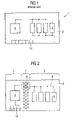
- FIG. 1 shows a conventional memory module having a buffer chip and a plurality of memory chips in accordance with the prior art
- FIG. 2 shows a memory module according to the invention in accordance with a first embodiment of the invention
- FIG. 3 shows a memory module having a cooling element in accordance with another embodiment of the present invention
- FIG. 4 shows a memory module having a web in accordance with another embodiment of the present invention.
- FIG. 5 shows a view of a printed circuit board for a memory module, in which the supply conductor surfaces of the first and second regions are thermally decoupled from one another.
- FIG. 1 shows a memory module 1 having a printed circuit board 2 on which a plurality of memory chips 3 and a buffer chip 4 are arranged.
- a printed circuit board 2 Arranged on the printed circuit board 2 are conductor tracks (not shown in detail) which connect the memory chips 3 to the buffer chip 4 and to an interface (which is applied to the printed circuit board 2 and is in the form of a plug connection 15 ) in a suitable manner in order to form the memory module 1 which can be driven by an external system.
- the memory module 1 is predominantly used to receive data from the external system, to store said data in the memory chips 3 , to read out data from the memory chips 3 and to provide the external system with said data.
- plug connector 15 it is also possible to provide any other type of connection contacts which can be used to permanently connect the printed circuit board 2 to the external system.
- FIG. 2 illustrates a memory module 1 in accordance with a first embodiment of the present invention.
- identical reference symbols relate to identical elements or elements having the same function.
- the memory chips 3 are arranged in a first region of the printed circuit board 2 and the buffer chip 4 is arranged in a second region 6 of the printed circuit board 2 .
- the printed circuit board 2 is illustrated as being essentially rectangular but it may also have any other desired shape.
- the intermediate region 7 is provided between the first region 5 and the second region 6 of the printed circuit board 2 .
- the intermediate region 7 has a number of passage holes 9 in order to reduce the thermal conductivity between the first region and the second region 6 .
- the passage holes reduce the cross-sectional area which is used to connect the first region to the second region, with the result that, given the same specific thermal conductivity of the printed circuit board 2 , a higher thermal resistance is achieved.
- the passage holes 9 are may not be metalized, with the result that the heat conduction between the first and second regions is not unnecessarily increased thereby.
- Conductor tracks 8 which are illustrated, by way of example, as connections between the buffer chip 4 and the memory chips 3 are routed around the passage holes 9 on the remaining webs.
- the holes are arranged in a plurality of rows between the first and second regions 5 , 6 in such a manner that they are offset with respect to one another.
- the diameter of the passage holes 9 and the distances between the passage holes 9 may be selected in such a manner that the mechanical stability of the printed circuit board is not impaired or is not considerably impaired.
- the passage holes 9 can be introduced using methods which are known to a person skilled in the art, such as boring, laser boring, depth etching or similar methods.
- the intermediate region 7 between the regions (which are thermally decoupled from one another) of the supply conductor surface 13 is configured in such a manner that the cross-sectional area of the supply conductor surface between the first and second regions 5 , 6 may be reduced by 50% or more in order to achieve considerable thermal decoupling.
- FIG. 3 illustrates another printed circuit board 2 according to one embodiment of the invention.
- holding elements 10 for a cooling element 11 are introduced into the passage holes 9 , said cooling element absorbing the heat transmitted in the intermediate region 7 in order to discharge it to the surrounding area.
- the cooling element 11 may be connected to another heat sink, for example a printed circuit board of the external system, a housing or another element, in order to dissipate heat.
- the cooling element may also be provided with a cooling-air fan or the like in order to achieve even better heat dissipation to the surrounding area.
- FIG. 4 illustrates another embodiment of the present invention.
- the first region 5 and the second region 6 are connected to one another by means of a narrow web 12 of the printed circuit board 2 .
- the narrow web 12 is formed in the intermediate region 7 of the printed circuit board 2 .
- a plurality of webs 12 may also be provided.
- cutouts extend from opposite edges of the printed circuit board 2 up to the web 12 which has a width that is sufficient to ensure the mechanical stability of the memory module 1 and which has a surface area that is sufficient to accommodate the connecting conductor tracks between the memory chips 3 and the buffer chip 4 .
- the position of the web 12 with respect to the first and second regions 5 , 6 can essentially be freely selected but a central arrangement of the web with respect to the width of the memory module is advantageous in order to minimize torsion moments which may act on the web.
- FIG. 5 illustrates another embodiment of the invention.
- the printed circuit board 2 of the memory module 1 has a supply conductor surface 13 which is provided either on a surface of the printed circuit board or in an intermediate layer of the printed circuit board 2 .
- the supply conductor surface 13 is used to provide a supply voltage with as little electrical resistance as possible at any location of the printed circuit board 2 at which the supply voltage is required by a chip that has been applied to said printed circuit board.
- the cutouts may be provided in the supply conductor surface 13 in order to insulate the contacts and the conductor track electrically from the supply conductor surface, or the contacts and conductor tracks are provided in another conductor track plane of the printed circuit board 2 .
- the latter is of two-part design in the embodiment of FIG. 5 .
- a first part of the supply conductor surface is arranged in the first region 5 and a second part of the supply conductor surface is arranged in the second region 6 of the printed circuit board 2 .
- the supply conductor surfaces 13 are connected to one another via conductive connecting webs 14 which are sufficiently large to provide the lowest possible electrical resistance but have a high thermal resistance. They may be implemented, for example, by means of webs between the first and second regions 5 , 6 of the supply conductor surface.
- the thermal decoupling of the supply conductor surfaces in the two regions 5 , 6 of the printed circuit board 2 leads to considerable thermal decoupling of the first and second regions 5 , 6 as compared to supply conductor surfaces which are configured, in a flat manner, from a metal layer that is very highly thermally conductive.
Landscapes
- Engineering & Computer Science (AREA)
- Power Engineering (AREA)
- Microelectronics & Electronic Packaging (AREA)
- Structure Of Printed Boards (AREA)
- Cooling Or The Like Of Electrical Apparatus (AREA)
Abstract
Description
Claims (21)
Applications Claiming Priority (2)
| Application Number | Priority Date | Filing Date | Title |
|---|---|---|---|
| DEDE102004041027.5 | 2004-08-25 | ||
| DE102004041027A DE102004041027B4 (en) | 2004-08-25 | 2004-08-25 | memory module |
Publications (2)
| Publication Number | Publication Date |
|---|---|
| US20060049515A1 US20060049515A1 (en) | 2006-03-09 |
| US7317248B2 true US7317248B2 (en) | 2008-01-08 |
Family
ID=35852345
Family Applications (1)
| Application Number | Title | Priority Date | Filing Date |
|---|---|---|---|
| US11/211,893 Expired - Fee Related US7317248B2 (en) | 2004-08-25 | 2005-08-25 | Memory module having memory chips protected from excessive heat |
Country Status (2)
| Country | Link |
|---|---|
| US (1) | US7317248B2 (en) |
| DE (1) | DE102004041027B4 (en) |
Cited By (10)
| Publication number | Priority date | Publication date | Assignee | Title |
|---|---|---|---|---|
| US20100290183A1 (en) * | 2008-01-31 | 2010-11-18 | Rijken Christopher N | Insulating Aperture In Printed Circuit Boards |
| US20150373827A1 (en) * | 2014-06-23 | 2015-12-24 | Huawei Technologies Co., Ltd. | Chip Heat Dissipation Structure and Terminal Device |
| JP2016033973A (en) * | 2014-07-31 | 2016-03-10 | アイシン・エィ・ダブリュ株式会社 | Power conversion device control board |
| USD780184S1 (en) * | 2013-03-13 | 2017-02-28 | Nagrastar Llc | Smart card interface |
| USD780763S1 (en) * | 2015-03-20 | 2017-03-07 | Nagrastar Llc | Smart card interface |
| USD792410S1 (en) * | 2013-03-13 | 2017-07-18 | Nagrastar Llc | Smart card interface |
| US20180079377A1 (en) * | 2015-03-27 | 2018-03-22 | Autonetworks Technologies, Ltd. | Vehicle-mounted power distribution board, electrical junction box, and charging/discharging controller |
| USD840404S1 (en) | 2013-03-13 | 2019-02-12 | Nagrastar, Llc | Smart card interface |
| USD864968S1 (en) | 2015-04-30 | 2019-10-29 | Echostar Technologies L.L.C. | Smart card interface |
| US20240015935A1 (en) * | 2021-09-30 | 2024-01-11 | Wuhan China Star Optoelectronics Semiconductor Display Technology Co., Ltd. | Supportive composite plate, fabrication method of the supportive composite plate, and display module |
Families Citing this family (7)
| Publication number | Priority date | Publication date | Assignee | Title |
|---|---|---|---|---|
| DE102006047627A1 (en) * | 2006-10-09 | 2008-04-10 | Robert Bosch Gmbh | Drive unit, and method for operating a drive unit |
| KR101344016B1 (en) * | 2007-07-31 | 2013-12-23 | 삼성전자주식회사 | Thermal-emitting Memory Module, Thermal-emitting Module Socket Electrically Connecting The Thermal-emitting Memory Module, Computer System Comprising The Thermal-emitting Memory Module And The Thermal-emitting Memory Module, And Method Of Using The Computer System Comprising The Same |
| DE102008037372A1 (en) * | 2008-09-18 | 2010-04-01 | Lear Corporation Gmbh | Housing for accommodation of e.g. connection interface, of motor vehicle, has accommodation chamber separated and thermally isolated from another accommodation chamber of housing, and recesses arranged at different side walls of housing |
| EP2442627A1 (en) * | 2010-10-15 | 2012-04-18 | Odelo GmbH | Motor vehicle light |
| DE102011107316A1 (en) | 2011-07-06 | 2013-06-06 | Abb Ag | Arrangement for cooling assemblies of an automation or control system |
| GB201700812D0 (en) * | 2017-01-17 | 2017-03-01 | British American Tobacco Investments Ltd | Apparatus for heating smokable material |
| DE102021201270A1 (en) * | 2021-02-10 | 2022-08-11 | Vitesco Technologies GmbH | Electronic assembly with at least a first electronic component and a second electronic component |
Citations (10)
| Publication number | Priority date | Publication date | Assignee | Title |
|---|---|---|---|---|
| DE4121545C2 (en) | 1991-06-28 | 1993-06-17 | Hella Kg Hueck & Co, 4780 Lippstadt, De | |
| US6205028B1 (en) | 1997-07-23 | 2001-03-20 | Sharp Kabushiki Kaisha | Circuit substrate including printed circuit board having heat-shielding portion |
| US20030107462A1 (en) * | 2001-12-10 | 2003-06-12 | Samsung Electro-Mechanics Co., Ltd. | Flyback transformer and device for holding bleeder resistor in such transformer |
| US20040012934A1 (en) * | 2002-07-16 | 2004-01-22 | Behdad Jafari | Multi-configuration processor-memory substrate device |
| US6787895B1 (en) * | 2001-12-07 | 2004-09-07 | Skyworks Solutions, Inc. | Leadless chip carrier for reduced thermal resistance |
| US20050018405A1 (en) * | 2003-07-24 | 2005-01-27 | Murata Manufacturing Co., Ltd. | Electronic apparatus |
| US20050035447A1 (en) * | 2003-01-15 | 2005-02-17 | Kyocera Corporation | Heat releasing member, package for accommodating semiconductor element and semiconductor device |
| US6940164B1 (en) * | 2000-08-18 | 2005-09-06 | Mitsubishi Denki Kabushiki Kaisha | Power module |
| US7031164B2 (en) * | 2002-08-29 | 2006-04-18 | Denso Corporation | Electronic circuit device including heat-generating element mounted on circuit board |
| US7124931B2 (en) * | 2003-11-18 | 2006-10-24 | Intel Corporation | Via heat sink material |
-
2004
- 2004-08-25 DE DE102004041027A patent/DE102004041027B4/en not_active Expired - Fee Related
-
2005
- 2005-08-25 US US11/211,893 patent/US7317248B2/en not_active Expired - Fee Related
Patent Citations (10)
| Publication number | Priority date | Publication date | Assignee | Title |
|---|---|---|---|---|
| DE4121545C2 (en) | 1991-06-28 | 1993-06-17 | Hella Kg Hueck & Co, 4780 Lippstadt, De | |
| US6205028B1 (en) | 1997-07-23 | 2001-03-20 | Sharp Kabushiki Kaisha | Circuit substrate including printed circuit board having heat-shielding portion |
| US6940164B1 (en) * | 2000-08-18 | 2005-09-06 | Mitsubishi Denki Kabushiki Kaisha | Power module |
| US6787895B1 (en) * | 2001-12-07 | 2004-09-07 | Skyworks Solutions, Inc. | Leadless chip carrier for reduced thermal resistance |
| US20030107462A1 (en) * | 2001-12-10 | 2003-06-12 | Samsung Electro-Mechanics Co., Ltd. | Flyback transformer and device for holding bleeder resistor in such transformer |
| US20040012934A1 (en) * | 2002-07-16 | 2004-01-22 | Behdad Jafari | Multi-configuration processor-memory substrate device |
| US7031164B2 (en) * | 2002-08-29 | 2006-04-18 | Denso Corporation | Electronic circuit device including heat-generating element mounted on circuit board |
| US20050035447A1 (en) * | 2003-01-15 | 2005-02-17 | Kyocera Corporation | Heat releasing member, package for accommodating semiconductor element and semiconductor device |
| US20050018405A1 (en) * | 2003-07-24 | 2005-01-27 | Murata Manufacturing Co., Ltd. | Electronic apparatus |
| US7124931B2 (en) * | 2003-11-18 | 2006-10-24 | Intel Corporation | Via heat sink material |
Non-Patent Citations (1)
| Title |
|---|
| German Patent Office Examination Report dated Jun. 13, 2005. |
Cited By (14)
| Publication number | Priority date | Publication date | Assignee | Title |
|---|---|---|---|---|
| US20100290183A1 (en) * | 2008-01-31 | 2010-11-18 | Rijken Christopher N | Insulating Aperture In Printed Circuit Boards |
| US8335077B2 (en) * | 2008-01-31 | 2012-12-18 | Hewlett-Packard Development Company, L.P. | Insulating aperture in printed circuit boards |
| USD840404S1 (en) | 2013-03-13 | 2019-02-12 | Nagrastar, Llc | Smart card interface |
| USD780184S1 (en) * | 2013-03-13 | 2017-02-28 | Nagrastar Llc | Smart card interface |
| USD792410S1 (en) * | 2013-03-13 | 2017-07-18 | Nagrastar Llc | Smart card interface |
| USD792411S1 (en) * | 2013-03-13 | 2017-07-18 | Nagrastar Llc | Smart card interface |
| USD949864S1 (en) * | 2013-03-13 | 2022-04-26 | Nagrastar Llc | Smart card interface |
| US20150373827A1 (en) * | 2014-06-23 | 2015-12-24 | Huawei Technologies Co., Ltd. | Chip Heat Dissipation Structure and Terminal Device |
| JP2016033973A (en) * | 2014-07-31 | 2016-03-10 | アイシン・エィ・ダブリュ株式会社 | Power conversion device control board |
| USD780763S1 (en) * | 2015-03-20 | 2017-03-07 | Nagrastar Llc | Smart card interface |
| US20180079377A1 (en) * | 2015-03-27 | 2018-03-22 | Autonetworks Technologies, Ltd. | Vehicle-mounted power distribution board, electrical junction box, and charging/discharging controller |
| US10442372B2 (en) * | 2015-03-27 | 2019-10-15 | Autonetworks Technologies, Ltd. | Vehicle-mounted power distribution board, electrical junction box, and charging/discharging controller |
| USD864968S1 (en) | 2015-04-30 | 2019-10-29 | Echostar Technologies L.L.C. | Smart card interface |
| US20240015935A1 (en) * | 2021-09-30 | 2024-01-11 | Wuhan China Star Optoelectronics Semiconductor Display Technology Co., Ltd. | Supportive composite plate, fabrication method of the supportive composite plate, and display module |
Also Published As
| Publication number | Publication date |
|---|---|
| DE102004041027A1 (en) | 2006-03-09 |
| DE102004041027B4 (en) | 2007-01-18 |
| US20060049515A1 (en) | 2006-03-09 |
Similar Documents
| Publication | Publication Date | Title |
|---|---|---|
| US7317248B2 (en) | Memory module having memory chips protected from excessive heat | |
| US6196002B1 (en) | Ball grid array package having thermoelectric cooler | |
| US5362986A (en) | Vertical chip mount memory package with packaging substrate and memory chip pairs | |
| US7542297B2 (en) | Optimized mounting area circuit module system and method | |
| KR100299002B1 (en) | Stacked semiconductor device | |
| US7910952B2 (en) | Power semiconductor arrangement | |
| US7602613B2 (en) | Thin module system and method | |
| US7446410B2 (en) | Circuit module with thermal casing systems | |
| US6943293B1 (en) | High power electronic package with enhanced cooling characteristics | |
| US20070258217A1 (en) | Split Core Circuit Module | |
| US20090052124A1 (en) | Circuit Module with Thermal Casing Systems | |
| US6646886B1 (en) | Power connection structure | |
| JP2818746B2 (en) | Cooling method for integrated circuits | |
| KR20080006016A (en) | Memory module system and method | |
| KR20010070141A (en) | Electronic module | |
| JP2001244391A5 (en) | ||
| US6184579B1 (en) | Double-sided electronic device | |
| US6195257B1 (en) | Apparatus and method of adapting a rectifier module to enhance cooling | |
| CN114597727B (en) | Terminal Fixing Method | |
| US20080032446A1 (en) | combination heat dissipation device with termination and a method of making the same | |
| JP4712948B2 (en) | Semiconductor device | |
| KR20010110341A (en) | Multi-chip module for use in high-power applications | |
| JP2006019660A (en) | Circuit board for surface mounting of power element | |
| KR102622520B1 (en) | Storage units and storage modules | |
| JP2007324544A (en) | Stacked semiconductor package |
Legal Events
| Date | Code | Title | Description |
|---|---|---|---|
| AS | Assignment |
Owner name: INFINEON TECHNOLOGIES AG, GERMANY Free format text: ASSIGNMENT OF ASSIGNORS INTEREST;ASSIGNOR:POECHMUELLER, PETER;REEL/FRAME:017149/0853 Effective date: 20051023 |
|
| FEPP | Fee payment procedure |
Free format text: PAYOR NUMBER ASSIGNED (ORIGINAL EVENT CODE: ASPN); ENTITY STATUS OF PATENT OWNER: LARGE ENTITY |
|
| STCF | Information on status: patent grant |
Free format text: PATENTED CASE |
|
| AS | Assignment |
Owner name: QIMONDA AG, GERMANY Free format text: ASSIGNMENT OF ASSIGNORS INTEREST;ASSIGNOR:INFINEON TECHNOLOGIES AG;REEL/FRAME:023806/0001 Effective date: 20060425 Owner name: QIMONDA AG,GERMANY Free format text: ASSIGNMENT OF ASSIGNORS INTEREST;ASSIGNOR:INFINEON TECHNOLOGIES AG;REEL/FRAME:023806/0001 Effective date: 20060425 |
|
| FPAY | Fee payment |
Year of fee payment: 4 |
|
| AS | Assignment |
Owner name: INFINEON TECHNOLOGIES AG, GERMANY Free format text: ASSIGNMENT OF ASSIGNORS INTEREST;ASSIGNOR:QIMONDA AG;REEL/FRAME:035623/0001 Effective date: 20141009 |
|
| FPAY | Fee payment |
Year of fee payment: 8 |
|
| AS | Assignment |
Owner name: POLARIS INNOVATIONS LIMITED, IRELAND Free format text: ASSIGNMENT OF ASSIGNORS INTEREST;ASSIGNOR:INFINEON TECHNOLOGIES AG;REEL/FRAME:036908/0923 Effective date: 20150708 |
|
| FEPP | Fee payment procedure |
Free format text: MAINTENANCE FEE REMINDER MAILED (ORIGINAL EVENT CODE: REM.); ENTITY STATUS OF PATENT OWNER: LARGE ENTITY |
|
| LAPS | Lapse for failure to pay maintenance fees |
Free format text: PATENT EXPIRED FOR FAILURE TO PAY MAINTENANCE FEES (ORIGINAL EVENT CODE: EXP.); ENTITY STATUS OF PATENT OWNER: LARGE ENTITY |
|
| STCH | Information on status: patent discontinuation |
Free format text: PATENT EXPIRED DUE TO NONPAYMENT OF MAINTENANCE FEES UNDER 37 CFR 1.362 |
|
| FP | Lapsed due to failure to pay maintenance fee |
Effective date: 20200108 |