US7313672B2 - Intellectual property module for system-on-chip - Google Patents
Intellectual property module for system-on-chip Download PDFInfo
- Publication number
- US7313672B2 US7313672B2 US11/048,595 US4859505A US7313672B2 US 7313672 B2 US7313672 B2 US 7313672B2 US 4859505 A US4859505 A US 4859505A US 7313672 B2 US7313672 B2 US 7313672B2
- Authority
- US
- United States
- Prior art keywords
- module
- signal
- handshake
- soc
- modules
- Prior art date
- Legal status (The legal status is an assumption and is not a legal conclusion. Google has not performed a legal analysis and makes no representation as to the accuracy of the status listed.)
- Expired - Fee Related, expires
Links
Images


Classifications
-
- G—PHYSICS
- G06—COMPUTING OR CALCULATING; COUNTING
- G06F—ELECTRIC DIGITAL DATA PROCESSING
- G06F15/00—Digital computers in general; Data processing equipment in general
- G06F15/16—Combinations of two or more digital computers each having at least an arithmetic unit, a program unit and a register, e.g. for a simultaneous processing of several programs
-
- B—PERFORMING OPERATIONS; TRANSPORTING
- B67—OPENING, CLOSING OR CLEANING BOTTLES, JARS OR SIMILAR CONTAINERS; LIQUID HANDLING
- B67C—CLEANING, FILLING WITH LIQUIDS OR SEMILIQUIDS, OR EMPTYING, OF BOTTLES, JARS, CANS, CASKS, BARRELS, OR SIMILAR CONTAINERS, NOT OTHERWISE PROVIDED FOR; FUNNELS
- B67C3/00—Bottling liquids or semiliquids; Filling jars or cans with liquids or semiliquids using bottling or like apparatus; Filling casks or barrels with liquids or semiliquids
- B67C3/02—Bottling liquids or semiliquids; Filling jars or cans with liquids or semiliquids using bottling or like apparatus
- B67C3/22—Details
- B67C3/26—Filling-heads; Means for engaging filling-heads with bottle necks
Definitions
- the present invention is concerned with an intellectual property (IP) module for a system-on-chip (SOC) which makes designing system architecture and integration easy.
- IP intellectual property
- SOC system-on-chip
- the SOC may be referred to as a semiconductor integrated circuit embedding main functions of the system in a single chip.
- the SOC generally includes hardware and software functional units, such as a memory, a processor, an external interface, an analogue and hybrid mode block, built-in software, an operating system (OS), and so forth.
- OS operating system
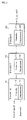
- FIG. 1 is a block diagram illustrating a functional architecture of a general SOC.
- a general SOC is composed of plural IP modules, 10 , 12 , and 14 , and a global central controller 20 which sends control signals to the IP modules, 10 , 12 , and 14 , in order to operate the IP modules in whole and stores timings and sequential orders of the control signals.
- the IP modules, 10 , 12 , and 14 receive the control signals that are in decoded forms from a global central controller 20 , and then perform different operations depending on input data.
- the global central controller 20 generates all the control signals, stores data about different states of the IP modules, 10 , 12 , and 14 , for a specific signal, and outputs control signals in sequence in response to requests from the IP modules, 10 , 12 , and 14 , after decoding an interrupt signal and external signals received.
- each of the IP modules, 10 , 12 , or 14 may be applicable to other SOCs that needs the function of the corresponding IP module, not limited to one SOC.
- a global central controller of the another SOC needs to preliminarily know the number of pipelining steps by the IP module in order to generate a signal for controlling the IP module in a correct order.
- the global central controller 20 controls all the IP modules 10 , 12 , and 14 , and needs to preliminarily know the information about the IP modules, 10 , 12 , and 14 , to generate control signals in correspondence with the information.
- a system operation time is lengthened and many difficulties are caused in mounting the IP module on another SOC.
- the present invention is directed to an IP module for an SOC, capable of easily transplanting an IP module and reducing a system operation time by distributed-controlling IP modules.
- An aspect of the invention to achieve the object is an IP module for a system-on-chip, which is comprised of: a controller for generating a control signal for IP module with reference to a handshake signal and sending a control signal which leads the IP module to process input data in response to handshake signal; and a data processor generating output data and a modified handshake signal after processing a handshake signal and input data under the control of the controller.
- FIG. 1 is a block diagram illustrating an functional architecture of a general SOC
- FIG. 2 is a block diagram illustrating an functional architecture of an SOC according to the present invention.
- FIGS. 3A through 3D are timing diagrams showing the kinds of handshaking signals necessary for IP modules mounted on the SOC.
- an asynchronous designing pattern is able to overcome the shortness of the synchronous pattern because it carries out data transmission by means of a handshake protocol, which is irrelevant to a delay time, without a global clock.
- the asynchronous SOC prosecutes data transmission by means of the handshake protocol, solving the problems of clock skewing, jittering, and power consumption and it improves the embedability and reusability of IP modules. Moreover, the asynchronous SOC provides stable data transmission among different IP modules by the handshake protocol and is advantageous to minimize various troubles arising in designing a large scale SOC.
- the present invention is relevant to IP modules necessary for designing such an asynchronous SOC.
- IP modules necessary for designing such an asynchronous SOC.
- FIG. 2 is a block diagram illustrating a functional architecture of an SOC according to the present invention.
- the SOC is composed of plural IP modules 100 , 200 , and 300 .
- the IP modules, 100 , 200 , and 300 each includes controllers, 110 , 210 , and 310 , and data processors 120 , 220 , and 320 , respectively.
- handshake signals are established by determining standard signals necessary for handshake protocols proposed for a specific IP module group and then control signals are generated on basis of the handshake signals.
- the standard signals for the handshake protocols are various in accordance with IP modules, while including all the signals processed in the IP modules, such as Image_Start, Block_Strobe, Image_End, and Scan_Start in the case of IP modules for image processing.
- FIGS. 3A through 3D are timing diagrams showing the types of handshaking signals necessary for IP modules mounted on the SOC.
- the Image_Start signal is used as the handshake signal to process input data of pixel data in the case of the IP module for image processing.
- the Block_Strobe signal is used as the handshake signal to process input data of pixel data in the case of the IP module for image processing.
- the Image_End signal is used as the handshake signal to process input data of pixel data in the case of the IP module for image processing.
- the Scan_Start signal is used as the handshake signal to process input data of pixel data in the case of the IP module for image processing.
- the handshake signal established for each IP module is transferred through the same pipelining step with which the input data is processed, and the path changes whenever there is a request for processing the input data.
- the handshake signals automatically vary according to the variations and therefore the sequential order of all control signals is maintained correct over all IP modules.
- Each control signal generated with reference to the handshake signals is stored in the controllers 110 , 210 , and 310 respectively, and the handshake signals preliminarily established are forced to be inputted in accordance with data flow in a designated pipeline of a corresponding IP module so that the data processors, 120 , 220 , and 320 , treat input data in compliance with the handshake signals.
- the data processors, 120 , 220 , and 320 generate output data and modified handshake signals from input data when the preliminary established handshake signals are applied thereto by the controllers 110 , 210 , and 310 .
- the output data and the modified handshake signal are applied to the IP module of the next stage.
- output data of the previous IP module is used as input data of the next IP module
- a modified handshake signal output from the previous IP module is used as a handshake signal for the next IP module.
- a handshake signal is fixed to a specific one of the IP modules, i.e., if the same handshake signal is always applied to a specific IP module, the handshake signal is usable with being normally stored in the controller of its corresponding IP module.
- the present invention determines all handshake signals used in IP modules, and generates control signals from the handshake signals and stores the control signals in the controllers. If there is a request for data processing, the controller makes the handshake signal be inputted to the IP module in compliance with the control signal preliminarily stored in the controller and thereby manages the data processor of the IP module to generate the output data and the modified handshake signal after processing the input data. The output data and the modified handshake signal are used as input data and a handshake signal for the next IP module.
- IP modules that are properly configured and easily reused by distributed-controlling the IP modules. Moreover, such IP modules are helpful for reducing effort and time for designing and verifying an SOC.
Landscapes
- Engineering & Computer Science (AREA)
- Computer Hardware Design (AREA)
- Theoretical Computer Science (AREA)
- Software Systems (AREA)
- Physics & Mathematics (AREA)
- General Engineering & Computer Science (AREA)
- General Physics & Mathematics (AREA)
- Information Transfer Systems (AREA)
- Semiconductor Integrated Circuits (AREA)
- Design And Manufacture Of Integrated Circuits (AREA)
Abstract
Description
Claims (2)
Applications Claiming Priority (2)
| Application Number | Priority Date | Filing Date | Title |
|---|---|---|---|
| KR10-2005-000757 | 2005-01-05 | ||
| KR1020050000757A KR100734521B1 (en) | 2005-01-05 | 2005-01-05 | IP Module for System-on-Chip |
Publications (2)
| Publication Number | Publication Date |
|---|---|
| US20060168314A1 US20060168314A1 (en) | 2006-07-27 |
| US7313672B2 true US7313672B2 (en) | 2007-12-25 |
Family
ID=36698378
Family Applications (1)
| Application Number | Title | Priority Date | Filing Date |
|---|---|---|---|
| US11/048,595 Expired - Fee Related US7313672B2 (en) | 2005-01-05 | 2005-02-01 | Intellectual property module for system-on-chip |
Country Status (2)
| Country | Link |
|---|---|
| US (1) | US7313672B2 (en) |
| KR (1) | KR100734521B1 (en) |
Families Citing this family (3)
| Publication number | Priority date | Publication date | Assignee | Title |
|---|---|---|---|---|
| DE102010003521A1 (en) * | 2010-03-31 | 2011-10-06 | Robert Bosch Gmbh | Modular structure for data processing |
| KR101781617B1 (en) | 2010-04-28 | 2017-09-25 | 삼성전자주식회사 | System on chip including unified input/output memory management unit |
| KR20180124340A (en) | 2017-05-11 | 2018-11-21 | 엘에스산전 주식회사 | Programmable logic controller |
Citations (6)
| Publication number | Priority date | Publication date | Assignee | Title |
|---|---|---|---|---|
| US5872988A (en) * | 1992-06-17 | 1999-02-16 | U.S. Philips Corporation | Parallel data processing device having a concatenated data path between elementary processors |
| US6052754A (en) * | 1998-05-14 | 2000-04-18 | Vlsi Technology, Inc. | Centrally controlled interface scheme for promoting design reusable circuit blocks |
| US6145073A (en) * | 1998-10-16 | 2000-11-07 | Quintessence Architectures, Inc. | Data flow integrated circuit architecture |
| KR20030030318A (en) | 2001-10-09 | 2003-04-18 | 이문기 | Universal bridge control structure |
| US20040236879A1 (en) * | 2003-05-23 | 2004-11-25 | Daren Croxford | Handling interrupts in a system having multiple data processing units |
| US7157934B2 (en) * | 2003-08-19 | 2007-01-02 | Cornell Research Foundation, Inc. | Programmable asynchronous pipeline arrays |
-
2005
- 2005-01-05 KR KR1020050000757A patent/KR100734521B1/en not_active Expired - Fee Related
- 2005-02-01 US US11/048,595 patent/US7313672B2/en not_active Expired - Fee Related
Patent Citations (6)
| Publication number | Priority date | Publication date | Assignee | Title |
|---|---|---|---|---|
| US5872988A (en) * | 1992-06-17 | 1999-02-16 | U.S. Philips Corporation | Parallel data processing device having a concatenated data path between elementary processors |
| US6052754A (en) * | 1998-05-14 | 2000-04-18 | Vlsi Technology, Inc. | Centrally controlled interface scheme for promoting design reusable circuit blocks |
| US6145073A (en) * | 1998-10-16 | 2000-11-07 | Quintessence Architectures, Inc. | Data flow integrated circuit architecture |
| KR20030030318A (en) | 2001-10-09 | 2003-04-18 | 이문기 | Universal bridge control structure |
| US20040236879A1 (en) * | 2003-05-23 | 2004-11-25 | Daren Croxford | Handling interrupts in a system having multiple data processing units |
| US7157934B2 (en) * | 2003-08-19 | 2007-01-02 | Cornell Research Foundation, Inc. | Programmable asynchronous pipeline arrays |
Non-Patent Citations (1)
| Title |
|---|
| Rower, T. etal, Intellectual Property Module of a Highly Parametrizable Embedded Stack Processor 1999, IEEE, pp. 399-403. * |
Also Published As
| Publication number | Publication date |
|---|---|
| KR20060080380A (en) | 2006-07-10 |
| KR100734521B1 (en) | 2007-07-03 |
| US20060168314A1 (en) | 2006-07-27 |
Similar Documents
| Publication | Publication Date | Title |
|---|---|---|
| US8275977B2 (en) | Debug signaling in a multiple processor data processing system | |
| US20100095138A1 (en) | Computer start-up timing control device and method thereof | |
| US8018784B2 (en) | Semiconductor device and data processor | |
| US10572438B1 (en) | Dynamic optimal data sampling time on a multi-drop bus | |
| US20080312900A1 (en) | Simulation apparatus and simulation method | |
| JPH0997177A (en) | Computer system interrupt control method | |
| US5951669A (en) | Method and apparatus for serialized interrupt transmission | |
| US11840181B2 (en) | In-vehicle communication device and method for starting up in-vehicle device | |
| US7313672B2 (en) | Intellectual property module for system-on-chip | |
| US7181559B2 (en) | Message based transport mechanism for level sensitive interrupts | |
| US20240094789A1 (en) | Reset domain control | |
| US20070220296A1 (en) | Data processing apparatus | |
| WO2024066950A1 (en) | Signal processing method, signal processing apparatus, chip, and electronic device | |
| US7590146B2 (en) | Information processing unit | |
| US20070156934A1 (en) | High-speed PCI Interface System and A Reset Method Thereof | |
| US6463551B1 (en) | Debug circuit and microcomputer incorporating debug circuit | |
| US7945718B2 (en) | Microcontroller waveform generation | |
| US7254735B2 (en) | Data processing system with block control circuits using self-synchronization handshaking and local clock/power control based on detected completion within subblocks | |
| US7454604B2 (en) | Reusable hardware IP protocol method for a system-on-chip device | |
| KR940001432B1 (en) | Peripheral system access method by meaus of td-bus | |
| JP2006163864A (en) | System LSI debugging method and apparatus | |
| KR20060112349A (en) | SOC bus system and bus data processing method | |
| JPH1049109A (en) | Liquid crystal display | |
| KR200298423Y1 (en) | Coordination logic for accessing peripherals from multiple processors | |
| JP2000003285A (en) | Method for processing interruption and circuit therefor |
Legal Events
| Date | Code | Title | Description |
|---|---|---|---|
| AS | Assignment |
Owner name: GWANGJU INSTITUTE OF SCIENCE AND TECHNOLOGY, KOREA Free format text: ASSIGNMENT OF ASSIGNORS INTEREST;ASSIGNORS:MUJAHID, FAHAD ALI;HAR, DONG-SOO;REEL/FRAME:016189/0669;SIGNING DATES FROM 20050218 TO 20050221 |
|
| STCF | Information on status: patent grant |
Free format text: PATENTED CASE |
|
| FEPP | Fee payment procedure |
Free format text: PAT HOLDER CLAIMS SMALL ENTITY STATUS, ENTITY STATUS SET TO SMALL (ORIGINAL EVENT CODE: LTOS); ENTITY STATUS OF PATENT OWNER: SMALL ENTITY |
|
| FEPP | Fee payment procedure |
Free format text: PAYOR NUMBER ASSIGNED (ORIGINAL EVENT CODE: ASPN); ENTITY STATUS OF PATENT OWNER: SMALL ENTITY |
|
| FPAY | Fee payment |
Year of fee payment: 4 |
|
| FEPP | Fee payment procedure |
Free format text: PAYER NUMBER DE-ASSIGNED (ORIGINAL EVENT CODE: RMPN); ENTITY STATUS OF PATENT OWNER: SMALL ENTITY Free format text: PAYOR NUMBER ASSIGNED (ORIGINAL EVENT CODE: ASPN); ENTITY STATUS OF PATENT OWNER: SMALL ENTITY |
|
| REMI | Maintenance fee reminder mailed | ||
| FPAY | Fee payment |
Year of fee payment: 8 |
|
| SULP | Surcharge for late payment |
Year of fee payment: 7 |
|
| FEPP | Fee payment procedure |
Free format text: MAINTENANCE FEE REMINDER MAILED (ORIGINAL EVENT CODE: REM.); ENTITY STATUS OF PATENT OWNER: SMALL ENTITY |
|
| LAPS | Lapse for failure to pay maintenance fees |
Free format text: PATENT EXPIRED FOR FAILURE TO PAY MAINTENANCE FEES (ORIGINAL EVENT CODE: EXP.); ENTITY STATUS OF PATENT OWNER: SMALL ENTITY |
|
| STCH | Information on status: patent discontinuation |
Free format text: PATENT EXPIRED DUE TO NONPAYMENT OF MAINTENANCE FEES UNDER 37 CFR 1.362 |
|
| FP | Lapsed due to failure to pay maintenance fee |
Effective date: 20191225 |