US7313181B2 - Calibration of scale factor in adaptive equalizers - Google Patents
Calibration of scale factor in adaptive equalizers Download PDFInfo
- Publication number
- US7313181B2 US7313181B2 US10/660,415 US66041503A US7313181B2 US 7313181 B2 US7313181 B2 US 7313181B2 US 66041503 A US66041503 A US 66041503A US 7313181 B2 US7313181 B2 US 7313181B2
- Authority
- US
- United States
- Prior art keywords
- increment
- threshold
- overflow count
- relationship
- filter
- Prior art date
- Legal status (The legal status is an assumption and is not a legal conclusion. Google has not performed a legal analysis and makes no representation as to the accuracy of the status listed.)
- Expired - Fee Related, expires
Links
Images


Classifications
-
- H—ELECTRICITY
- H04—ELECTRIC COMMUNICATION TECHNIQUE
- H04L—TRANSMISSION OF DIGITAL INFORMATION, e.g. TELEGRAPHIC COMMUNICATION
- H04L25/00—Baseband systems
- H04L25/02—Details ; arrangements for supplying electrical power along data transmission lines
- H04L25/03—Shaping networks in transmitter or receiver, e.g. adaptive shaping networks
- H04L25/03006—Arrangements for removing intersymbol interference
- H04L25/03012—Arrangements for removing intersymbol interference operating in the time domain
- H04L25/03019—Arrangements for removing intersymbol interference operating in the time domain adaptive, i.e. capable of adjustment during data reception
- H04L25/03038—Arrangements for removing intersymbol interference operating in the time domain adaptive, i.e. capable of adjustment during data reception with a non-recursive structure
-
- H—ELECTRICITY
- H03—ELECTRONIC CIRCUITRY
- H03H—IMPEDANCE NETWORKS, e.g. RESONANT CIRCUITS; RESONATORS
- H03H21/00—Adaptive networks
- H03H21/0012—Digital adaptive filters
- H03H21/0043—Adaptive algorithms
- H03H2021/0056—Non-recursive least squares algorithm [LMS]
- H03H2021/0065—Sign-sign LMS
-
- H—ELECTRICITY
- H03—ELECTRONIC CIRCUITRY
- H03H—IMPEDANCE NETWORKS, e.g. RESONANT CIRCUITS; RESONATORS
- H03H21/00—Adaptive networks
- H03H21/0001—Analogue adaptive filters
-
- H—ELECTRICITY
- H04—ELECTRIC COMMUNICATION TECHNIQUE
- H04L—TRANSMISSION OF DIGITAL INFORMATION, e.g. TELEGRAPHIC COMMUNICATION
- H04L25/00—Baseband systems
- H04L25/02—Details ; arrangements for supplying electrical power along data transmission lines
- H04L25/03—Shaping networks in transmitter or receiver, e.g. adaptive shaping networks
- H04L25/03006—Arrangements for removing intersymbol interference
- H04L2025/03433—Arrangements for removing intersymbol interference characterised by equaliser structure
- H04L2025/03439—Fixed structures
- H04L2025/03445—Time domain
- H04L2025/03471—Tapped delay lines
- H04L2025/03477—Tapped delay lines not time-recursive
Definitions
- the present invention relates to communication circuits, and more particularly, a circuit for adaptive equalization of a communication channel.
- FIG. 1 provides a high-level abstraction of a portion of a computer server or system, where microprocessor 102 resides on board 104 and communicates with memory 106 on board 108 . The communication is by way of striplines on backplane 110 . Backplane 110 is connected to boards 104 and 108 by connectors 112 . Not shown in FIG. 1 are other memory units and microprocessors, where the various microprocessors and memory units may communicate to one another so as to access or write data and instructions.
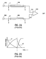
- FIG. 2 a shows drivers 202 and 204 driving transmission lines 206 and 208 , respectively.
- drivers 202 and 204 drive their respective transmission lines to complementary voltages.
- Typical curves for the node voltages at nodes n 1 and n 2 for a bit transition are provided in FIG. 2 b , where the bit transition is indicated by a dashed vertical line crossing the time axis.
- the information content is provided by the difference in the two node voltages.
- the signal-to-noise ratio is relatively large. If the transmission lines are linear, time-invariant systems having a bandwidth significantly greater than that of the transmitted signal, then a relatively simple receiver architecture may be employed to recover the transmitted data. Such a receiver is abstracted by comparator 210 , which provides a logic signal in response to the difference in the two received voltages at ports 212 and 214 .
- every transmission line has a finite bandwidth, and for signal bandwidths that are comparable to or exceed the transmission line (channel) bandwidth, intersymbol interference may present a problem.
- actual transmission lines may have dispersion, whereby different spectral portions of a signal travel at different speeds. This may result in pulse spreading, again leading to intersymbol interference.
- the transmission lines used with backplanes or motherboards are such that intersymbol interference is present.
- Channel equalization is a method in which one or more filters are employed to equalize the channel to help mitigate intersymbol interference.
- filters may be sampled-data (discrete-time) filters, where a time index t is a discrete variable, or they may be continuous-time filters, where the time index is a continuous variable.
- Many channel equalizers are realized by a Finite Impulse Response (FIR) filter employed at the receiver.
- FIR Finite Impulse Response
- FIG. 3 is an abstraction of a FIR filter structure, where x(t) is the input (received) signal to the FIR filter and z(t) is the filtered output. In the case of differential signaling, x(t) and z(t) may be viewed as representing differential signals.
- Multipliers 302 and summer 304 may be realized in the analog or digital domain. For the embodiments described in these letters patent, multipliers 302 and summer 304 are realized in the analog domain.
- the filter vector is updated during a training time interval, and then remains fixed for some period of time.
- a known sequence is transmitted over a communication channel to the receiver, and the filter vector is synthesized during the training time interval.
- Many algorithms have been developed to synthesize the filter vector.
- LMS Least Mean Square
- the well-known LMS (Least Mean Square) algorithm is an iterative technique based upon the method of steepest descent (gradient) to minimize a squared error.
- the filter weights assume discrete values limited to some fixed range, and the scale factor K takes into account this finite range of the filter weights as well as practical implementations of the filtering.
- the known training sequence d(t) may take on either of the values V CC or ⁇ V CC , where V CC is a supply voltage, but in practice the filtered output z(t) is always in magnitude less than the supply voltage. In this case, K ⁇ 1.
- h ( t +1) h ( t )+ ⁇ sgn ⁇ [Kd ( t ) ⁇ z ( t )] ⁇ sgn ⁇ x ( t ) ⁇ , where sgn ⁇ ⁇ is the sign function.
- the sign-sign-LMS algorithm although widely used due to its simplicity of implementation, has been found to have some undesirable properties when used in adaptive high-speed equalizers with relatively low to moderate length words (e.g., four to six bits) for the filter weights. Because the probability of filter weight update during adaptation is high, there is a significant amount of residual noise in the filter weights, even after convergence of the algorithm.
- This residual noise may be reduced by choosing a longer window (smaller ⁇ ), but this increases the convergence time, or in other words, the training time interval.
- Another disadvantage found in many instances is that the converged filter weights are relatively sensitive to the scale factor K, whose optimum value has been found to be difficult to determine.
- FIG. 1 is a high-level abstraction of a server system, illustrating signaling between boards via a backplane.
- FIG. 2 a illustrates differential signaling on two transmission lines.
- FIG. 2 b shows typical voltage curves representing differential signaling on the transmission lines of FIG. 2 a.
- FIG. 3 illustrates a finite impulse response (FIR) filter, or tap delay-line.
- FIR finite impulse response
- FIG. 4 illustrates a circuit at a high-level functional level for implementing adaptive equalization as taught in these letters patent.
- FIG. 5 illustrates a circuit at a high-level functional level for implementing multiplication in the analog domain for the circuit of FIG. 4 .
- FIG. 6 is a more detailed illustration of the circuit of FIG. 5 for the special case of 2-bit multiplier weights.
- FIG. 7 is a circuit for a differential latch that may be used in the circuit of FIG. 4 .
- FIG. 8 is a flow diagram illustrating a method for calibrating the scale factor used in the circuit of FIG. 4 .
- FIG. 9 illustrates a circuit at a high-level functional level for implementing the calibration method of FIG. 8 for the adaptive equalizer of FIG. 4 .
- FIG. 10 illustrates a circuit at a high-level functional level for implementing the calibration method of FIG. 8 for a wide class of adaptive equalizers.
- FIG. 4 provides an abstraction of an embodiment of the present invention.
- Each filter weight is represented by a set of discrete voltages taking on either 0 or V CC (LOW or HIGH), so that each filter weight may be viewed as a discrete variable in the digital domain represented by a finite number of bits. However, the filtering is performed in the analog domain so that the filtered output z(t) is an analog voltage signal. If differential signaling is employed, then both analog voltages x(t) and z(t) are differential signals.
- Data symbol generator 404 provides a sequence of voltages in the digital domain representing sgn ⁇ d(t) ⁇ . Because sgn ⁇ ⁇ obviously assumes only one of two values, the sequence of voltages representing sgn ⁇ d(t) ⁇ may be viewed as a sequence of binary values 0 or 1, which may be stored in a memory unit or generated by a finite state machine. Data symbol generator 404 also provides a sequence of voltages in the digital domain representing d(t). In digital communications, the transmitted symbols range over a finite set, so that (remembering that d(t) is the transmitted training sequence) each d(t) may be represented by a finite number of bits. These bits may be stored in memory, or generated by a finite machine.
- Symbol-to-voltage converter 406 converts the digital domain voltages representing d(t) into analog voltages representing d(t). For example, consider the case in which differential bipolar signaling is employed. In this case, only one bit of information, for example a voltage 0 or V CC , is needed to represent d(t) and is provided to the input of symbol-to-voltage converter 406 , and two voltages are used to represent the differential output voltage of symbol-to-voltage converter 406 . For example, in this case, symbol-to-voltage converter 406 may provide the differential voltage [0, V CC ] in response to one of its input voltages, say 0, and the differential voltage [V CC , 0] in response to the input voltage V CC . Such a circuit is of course obvious, and for the more general case, circuits for symbol-to-voltage converter 406 are straightforward to implement.
- Multiplier 408 multiplies the analog voltage d(t) by the negative of the scale factor, ⁇ K. This multiplication is performed in the analog domain, but just as for the filter h (t), the scale factor is represented by a set of discrete voltages taking on the values 0 or V CC (LOW or HIGH), so that K is represented by a finite number of bits.
- Summer 410 adds the analog voltage ⁇ Kd(t) to the filtered output z(t), which is provided to the input of comparator 412 .
- the multiplier 408 and summer 410 have the same structure as a filter tap, so that an example circuit for multiplier 408 and summer 410 is described later in connection with FIR 402 .
- Comparator 412 provides a logic output signal indicative of the difference of its two input signals (each input signal is part of a differential voltage in the differential signaling case), so that it outputs sgn ⁇ z(t) ⁇ Kd(t) ⁇ as a discrete voltage 0 or V CC (LOW or HIGH) in the digital domain. (It is immaterial whether comparator 412 evaluates sgn ⁇ 0 ⁇ as a LOW or HIGH voltage.) Comparator 412 also includes a latch for latching its output voltage. (For simplicity, clock signals are not shown in FIG.
- Multiplier 414 and summer 416 effectively subtract sgn ⁇ z(t) ⁇ Kd(t) ⁇ from sgn ⁇ d(t) ⁇ , and multiplier 418 multiplies this difference by the filter memory parameter ⁇ , which is then provided as an operand to multiplier 424 .
- the data vector x (t) is provided to comparator 426 , which outputs the vector sgn ⁇ x (t) ⁇ as an operand to multiplier 424 .
- Comparator 426 also includes a latch.
- the data vector x (t) may be provided by FIR 402 because this vector is also used by FIR 402 to perform filtering.
- the values of x (t) may be obtained by samplers, not shown for simplicity.
- Multiplier 424 multiplies its two operands together, so that each component of sgn ⁇ x (t) ⁇ is multiplied by the scalar ⁇ [sgn ⁇ d(t) ⁇ sgn ⁇ z(t) ⁇ Kd(t) ⁇ ], and this result is provided to summer 420 .
- Summer 420 , delay element 422 , and the feedback from delay element 422 to summer 420 perform the desired iteration on the filter weights as expressed by equation (1).
- the filter weights for equalization are given by h (T), in which case FIR 402 may be disconnected from the circuit so as to provide the equalized output z(t) for t>T.
- Multipliers 414 and 418 , summers 416 and 420 , and unit delay shift 422 operate in the digital domain, whereas the multiplications and summation performed within FIR 402 , as well as summer 410 and multiplier 408 , are performed in the analog domain.
- the multiplication weights h (t) and K in FIG. 4 are discrete-valued signals (i.e., digital signals) represented by a finite number of bits (HIGH and LOW voltages).
- d(t) is a discrete-valued signal due because of the nature of digital communication, it is nevertheless viewed as an analog signal because it is a differential voltage input to a voltage-to-current converter when performing the multiplication indicated by multiplier 408 , as described later.
- Circuits for performing operations in the digital domain i.e., logic circuits
- a circuit implementation for performing the analog filtering (multiplication and summation) in FIG. 4 is now described below.
- FIG. 5 A circuit to implement multiplication in the analog domain utilizing differential signals is shown in FIG. 5 , where the differential signal voltage x(t), represented by the two voltages ⁇ x + (t), x ⁇ (t) ⁇ , is effectively multiplied by [ h ] i , the i th component of the filter vector h . Multiplication by [ h ] i also involves its bit-wise logical complement, denoted as [ h ] i c , which is easily generated.
- the multiplier indicated by FIG. 5 comprises voltage-to-current converter 502 and current steering DAC (digital-to-analog converter) 504 .
- Current steering DAC 504 steers currents ⁇ [ h ] i I ⁇ and ⁇ [ h ] i I + , respectively, to loads 506 and 508 , and shunts the rest of the current (if any) to ground.
- the voltage developed at nodes 510 and 512 are, respectively, Z L ⁇ [ h ] i I ⁇ and Z L ⁇ [ h ] i I + , where Z L is the impedance of loads 506 and 508 .
- the difference in voltages developed at nodes 512 and 510 is given by ⁇ Z L ⁇ [ h ] i (V + ⁇ V ⁇ ).
- the difference in voltages developed at node 512 and 512 is seen to be proportional to the desired multiplication [ h ] i (V + ⁇ V ⁇ ) where the proportionality is the dimensionless scalar ⁇ Z L ⁇ . This dimensionless scalar is not of theoretical concern because it is taken into account by the scale factor K when performing the filter weight update.
- FIG. 6 An example of voltage-to-current converter 502 and current steering DAC 504 at the circuit level is shown in FIG. 6 .
- b 1 and b 0 are voltages representing binary variables, where a HIGH voltage represents the value 1 and a LOW voltage represents the value 0.
- b 1 and b 0 also represent binary variables, where b 1 c and b 0 c are, respectively, the logical complements of b 1 and b 0 .
- the differential voltage ⁇ x + (t), x ⁇ (t) ⁇ is applied to input ports 602 and 604 .
- Current source 602 provides bias current to a differential pair comprising pMOSFETs 608 , 610 , 612 , and 614 .
- the gates of pMOSFETs 608 and 610 are connected to input port 602
- the gates of pMOSFETs 612 and 614 are connected to input port 604 .
- the combination of pMOSFET 608 to pMOSFET 610 looks like a classical cascode pair, save for the fact that the gate of pMOSFET 608 is not at a fixed voltage.
- the voltage-to-current converter of FIG. 6 may be termed an active cascode voltage-to-current converter.
- the betas of pMOSFET 608 and 610 may be chosen such that the active cascode configuration of pMOSFETs 608 and 610 forces pMOSFET 608 to operate in the triode region when pMOSFET 610 is in its active region.
- V S2 denote the source voltage of pMOSFET 610
- V S1 denote the source voltage of pMOSFET 608 .
- V S2 >V g +
- V GT is defined as V S1 ⁇ V g ⁇
- pMOSFETs 608 and 612 With pMOSFETs 608 and 612 operating in the triode region, they act approximately as resistors to degenerate pMOSFETs 610 and 614 , respectively.
- Degeneration provides a relationship between the voltage difference x + (t) ⁇ x ⁇ (t) and the current difference I + ⁇ I ⁇ that is linear over a wider range than if degeneration was not present.
- I + is the drain-source current for pMOSFETs 608 and 610
- I ⁇ is the drain-source current of pMOSFETs 612 and 614 , respectively.
- summer 410 The addition operation indicated by summer 410 is implemented by connecting the output ports of each current steering DAC for FIR 402 and multiplier 408 to loads 506 and 508 . Which particular loads these output ports are connected to determine the sign of the multiplier. For example, without loss of generality, we may take a positive multiplicative weight to be implemented by connecting the output port in the I + current path to load 508 and the output port in the I ⁇ current path to load 506 . Then, to implement multiplication by a negative weight, the output port in the I + current path is connected to load 506 and the output port in the I ⁇ current path to load 508 .
- FIG. 7 The combination of loads 506 and 508 ( FIGS. 5 and 6 ) and comparator 412 ( FIG. 4 ) may be realized by the circuit of FIG. 7 , which may be referred to as an active cascode differential latch.
- nMOSFETs 714 and 716 play the role of active cascode transistors, although they are not cascode transistors in the classical sense because their gate voltages are not biased to a constant voltage.
- Input port 702 is connected to node 512 and input port 704 is connected to node 510 .
- a clock signal in FIG. 7 is denoted by ⁇ .
- pre-charge transistor 722 When clock signal ⁇ is HIGH, pre-charge transistor 722 provides a low impedance path between the gates of transistors 710 and 712 , pre-charging the differential latch so that the output voltages at output ports 706 and 708 are forced to be substantially equal to one another.
- clock signal ⁇ When clock signal ⁇ is LOW, pre-charge transistor 722 switches OFF to put the differential latch in an evaluation mode, where a differential voltage at output ports 706 and 708 develops in response to the currents (or voltages) at input ports 702 and 704 .
- Cross coupled pMOSFETs 718 and 720 are connected as a latch, so that the differential voltages developed at output ports 706 and 708 are amplified to a complementary logic levels.
- the resulting complementary voltages may both be used in subsequent digital processing, or only one of the complementary voltages may be used. For example, dual rail logic may be employed in some or all of the subsequent digital processing.
- nMOSFETs 710 and 712 operate in their triode regions and nMOSFETs 714 and 716 operate in their active regions.
- the differential latch of FIG. 7 has a relatively low input impedance, and furthermore, these nMOSFETs require a relatively small amount of headroom voltage. This may be important as supply voltages are scaled lower and lower, because voltage headroom for analog circuit blocks may be a critical issue.
- a small headroom voltage requirement also improves the input common-mode voltage range of the stages previous to the differential latch, i.e., the voltage-to-current converters and current steering DACs.
- the scale factor K takes into account various scaling factors due to the communication channel and circuit implementation.
- the scale factor K affects the available noise margin, so it is important to set its value appropriately.
- the optimal value for K depends on the communication channel characteristics, which usually are not known a priori.
- a relatively simple method for calibrating K making use of a received training sequence is shown in the flow diagram of FIG. 8 .
- K is initialized to zero.
- the filter is updated over a training sequence. During this update, a count is made of the number of overflows in the components of the filter vector.
- the overflow count is compared to a threshold ⁇ . If the overflow count is greater than ⁇ , control is brought to block 808 , in which case the current value for K is decremented by ⁇ and the calibration ends. If the overflow count is less than ⁇ , control is brought to block 810 where K is incremented by ⁇ , and control is brought to block 804 to begin another update sequence for the filter weights with the new value for K.
- Block 806 may be modified to shift control to block 808 if the overflow count is greater than or equal to the threshold ⁇ .
- the overflow count threshold ⁇ and scale factor calibration increment ⁇ are chosen before calibration is performed. These scalars may be determined offline via simulations with expected communication channels. In some embodiments, the overflow count threshold may be set to a value less than 1% of the length of the training sequence.
- the calibration increment trades off coarseness with the number of times block 804 is performed. In practice, calibration of the scale factor need not be performed very often, and may in some instances be performed only once for a communication channel.
- FIG. 9 A hardware implementation for the calibration method of FIG. 8 is shown at a high-level in FIG. 9 .
- Many of the functional units shown in FIG. 9 have equivalents in FIG. 4 and are labeled accordingly with the same numerals. These functional units need not be described again.
- functional units 404 and 406 in FIG. 4 have been combined into functional unit 902 .
- FIG. 5 also includes overflow counter 904 , finite state machine (FSM) 906 , multiplexer 908 , summer 910 , delay element 912 , and summer 914 .
- FSM finite state machine
- FIG. 9 calibration of K adds only a modest amount of hardware to implementing the filter update.
- Summer 914 is similar to summer 420 in FIG. 4 , but a different numerical label is used to emphasize that summer 914 provides an overflow signal to overflow counter 904 to indicate when a numerical overflow occurs during summation.
- Overflow counter 904 keeps track of the number of numerical overflows during a training sequence period (block 804 ).
- FSM 906 initializes overflow counter 904 before the beginning of a training sequence, and controls data generator 902 to begin generating a sequence of data symbols when a new iteration on a training sequence begins.
- Functional units 908 , 910 , and 912 perform either block 808 or block 810 .
- Delay element 912 indicates a delay of L, which denotes the length of a training sequence. If at the end of a training sequence the overflow counter indicates that the overflow count is greater than the threshold ⁇ , FSM 906 sends a control signal to multiplexer 908 so that ⁇ is added to the current value of K for use in the next training sequence. Otherwise, ⁇ is added to the current value of K. As discussed with respect to block 806 , this procedure may be modified so that ⁇ is added when the overflow count is greater than or equal to the threshold ⁇ .
- filter increment generator 1002 receives as input the difference z(t) ⁇ Kd(t) from summer 410 and the received data vector x (t) from FIR 402 , and outputs to summer 914 the increment vector ⁇ h (t) that is to be summed with the current filter vector h (t) to arrive at the updated filter vector h (t+1).
- Data generator 1002 is labeled with a different numeral to indicate that it may or may not provide data information, such as sgn ⁇ d(t) ⁇ , to filter increment generator 1002 .
- nMOSFETs replace pMOSFETs
- pMOSFETs replace nMOSFETs
- Other circuit structures for performing multiplication and summation in the analog domain may be employed. Indeed, the multiplication and summation may also be performed entirely in the digital domain, although such circuit implementations, which would require analog-to-digital converters, may at this time not be practical for high-speed communication channels.
- the partitioning of a circuit into simpler, functional units is somewhat arbitrary, and the particular functional units disclosed here are not meant to limit the scope of the invention.
- Various functional units may be combined into more complicated functional units, and functional units may be partitioned into simpler functional units.
- An example is the combining of functional units 404 and 406 of FIG. 4 into data generator functional unit 902 of FIG. 9 .
- the various summers and multipliers disclosed here may be re-arranged as implied by arithmetic commutative and associative laws.
- the term “summer” also may mean a functional unit for performing a differencing operation.
- a digital summer may comprise more than one summer to operate on more than one pair of operands in parallel.
- a delay element may comprise more than one delay elements to delay more than one value in parallel. Similar remarks apply to multipliers and latches.
- training sequences for the calibration may be a repetition of a training sequence, or segments of one long training sequence.
- the increment used in block 808 of FIG. 8 need not be the same increment as that used in block 810 , an the increment may be made to vary each time control is brought to block 802 .
Abstract
Description
where
where sgn{ } is the sign function. The sign-sign-LMS algorithm, although widely used due to its simplicity of implementation, has been found to have some undesirable properties when used in adaptive high-speed equalizers with relatively low to moderate length words (e.g., four to six bits) for the filter weights. Because the probability of filter weight update during adaptation is high, there is a significant amount of residual noise in the filter weights, even after convergence of the algorithm. This residual noise may be reduced by choosing a longer window (smaller μ), but this increases the convergence time, or in other words, the training time interval. Another disadvantage found in many instances is that the converged filter weights are relatively sensitive to the scale factor K, whose optimum value has been found to be difficult to determine.
which may be termed the conditional update sign-sign LMS algorithm.
Each filter weight is represented by a set of discrete voltages taking on either 0 or VCC (LOW or HIGH), so that each filter weight may be viewed as a discrete variable in the digital domain represented by a finite number of bits. However, the filtering is performed in the analog domain so that the filtered output z(t) is an analog voltage signal. If differential signaling is employed, then both analog voltages x(t) and z(t) are differential signals. An example of
Claims (18)
Priority Applications (3)
| Application Number | Priority Date | Filing Date | Title |
|---|---|---|---|
| US10/660,415 US7313181B2 (en) | 2003-09-10 | 2003-09-10 | Calibration of scale factor in adaptive equalizers |
| PCT/US2004/029055 WO2005027445A1 (en) | 2003-09-10 | 2004-09-03 | Calibration of scale factor in adaptative equalizers |
| TW093127273A TWI296170B (en) | 2003-09-10 | 2004-09-09 | Calibration of scale factor in adaptive equalizers |
Applications Claiming Priority (1)
| Application Number | Priority Date | Filing Date | Title |
|---|---|---|---|
| US10/660,415 US7313181B2 (en) | 2003-09-10 | 2003-09-10 | Calibration of scale factor in adaptive equalizers |
Publications (2)
| Publication Number | Publication Date |
|---|---|
| US20050053126A1 US20050053126A1 (en) | 2005-03-10 |
| US7313181B2 true US7313181B2 (en) | 2007-12-25 |
Family
ID=34227061
Family Applications (1)
| Application Number | Title | Priority Date | Filing Date |
|---|---|---|---|
| US10/660,415 Expired - Fee Related US7313181B2 (en) | 2003-09-10 | 2003-09-10 | Calibration of scale factor in adaptive equalizers |
Country Status (3)
| Country | Link |
|---|---|
| US (1) | US7313181B2 (en) |
| TW (1) | TWI296170B (en) |
| WO (1) | WO2005027445A1 (en) |
Cited By (5)
| Publication number | Priority date | Publication date | Assignee | Title |
|---|---|---|---|---|
| US20070002942A1 (en) * | 2005-03-03 | 2007-01-04 | Richard Simpson | Equalization circuit |
| US20070053419A1 (en) * | 2005-09-02 | 2007-03-08 | Park Sung K | Adaptive analog equalizer and digital signal receiver having the same |
| US20120264380A1 (en) * | 2011-03-14 | 2012-10-18 | Nujira Limited | Polar Amplification Transmitter Distortion Reduction |
| US8680939B2 (en) | 2011-10-20 | 2014-03-25 | Lockheed Martin Corporation | Differential equalizer and system, method, and computer program product thereof |
| US20150163076A1 (en) * | 2013-12-11 | 2015-06-11 | Thales | Iterative method for synthesizing digital filters for shaping a signal |
Families Citing this family (5)
| Publication number | Priority date | Publication date | Assignee | Title |
|---|---|---|---|---|
| DE102011052881B4 (en) * | 2011-08-22 | 2018-05-17 | Robert Bosch Automotive Steering Gmbh | Method for determining a rack-and-pinion force for a steering device in a vehicle, steering device and control and / or regulating device for a steering device |
| US10181860B1 (en) | 2017-10-26 | 2019-01-15 | Analog Devices Global Unlimited Company | Reducing residue signals in analog-to-digital converters |
| US10187075B1 (en) * | 2018-05-08 | 2019-01-22 | Analog Devices Global Unlimited Company | Blocker tolerance in continuous-time residue generating analog-to-digital converters |
| US10361711B1 (en) | 2018-12-13 | 2019-07-23 | Analog Devices Global Unlimited Company | Stub filters to improve blocker tolerance in continuous-time residue generation analog-to-digital converters |
| CN109921763B (en) * | 2019-02-26 | 2021-10-22 | 华南理工大学 | FIR filter for reducing multipliers and output calculation method thereof |
Citations (11)
| Publication number | Priority date | Publication date | Assignee | Title |
|---|---|---|---|---|
| US4491930A (en) * | 1970-12-28 | 1985-01-01 | Hyatt Gilbert P | Memory system using filterable signals |
| US6111878A (en) * | 1997-11-04 | 2000-08-29 | Alcatel | Low jitter timing recovery technique and device for asynchronous transfer mode (ATM) constant bit rate (CBR) payloads |
| US6240134B1 (en) * | 1997-09-30 | 2001-05-29 | Alcatel | Method for stabilizing the operation of fractionally spaced sequalizer in digital signal receivers |
| US6286021B1 (en) * | 1997-10-22 | 2001-09-04 | Texas Instruments Incorporated | Apparatus and method for a reduced complexity tap leakage unit in a fast adaptive filter circuit |
| TW498637B (en) | 2000-05-11 | 2002-08-11 | Hitachi Ltd | Adaptive equalizer circuit |
| US6618740B1 (en) | 1998-12-31 | 2003-09-09 | Texas Instruments Incorporated | Method and architecture for controlling asymmetry of an LMS adaptation algorithm that controls FIR filter coefficients |
| US6621330B1 (en) * | 2002-06-04 | 2003-09-16 | Intel Corporation | Discrete-time analog filter |
| US6771717B1 (en) * | 1999-10-22 | 2004-08-03 | Nokia Mobile Phones Ltd. | Arrangement and method for restricting word length |
| US20050163331A1 (en) * | 1998-09-30 | 2005-07-28 | Gao Shawn X. | Band-limited adaptive feedback canceller for hearing aids |
| US6985492B1 (en) * | 1999-04-13 | 2006-01-10 | Broadcom Corporation | Voice gateway with voice synchronization |
| US7079576B2 (en) * | 2001-05-24 | 2006-07-18 | Frank Patrick Bologna | Joint zero-forcing and matched-filter adaptive digital equalizer |
-
2003
- 2003-09-10 US US10/660,415 patent/US7313181B2/en not_active Expired - Fee Related
-
2004
- 2004-09-03 WO PCT/US2004/029055 patent/WO2005027445A1/en active Application Filing
- 2004-09-09 TW TW093127273A patent/TWI296170B/en not_active IP Right Cessation
Patent Citations (12)
| Publication number | Priority date | Publication date | Assignee | Title |
|---|---|---|---|---|
| US4491930A (en) * | 1970-12-28 | 1985-01-01 | Hyatt Gilbert P | Memory system using filterable signals |
| US6240134B1 (en) * | 1997-09-30 | 2001-05-29 | Alcatel | Method for stabilizing the operation of fractionally spaced sequalizer in digital signal receivers |
| US6286021B1 (en) * | 1997-10-22 | 2001-09-04 | Texas Instruments Incorporated | Apparatus and method for a reduced complexity tap leakage unit in a fast adaptive filter circuit |
| US6111878A (en) * | 1997-11-04 | 2000-08-29 | Alcatel | Low jitter timing recovery technique and device for asynchronous transfer mode (ATM) constant bit rate (CBR) payloads |
| US20050163331A1 (en) * | 1998-09-30 | 2005-07-28 | Gao Shawn X. | Band-limited adaptive feedback canceller for hearing aids |
| US6618740B1 (en) | 1998-12-31 | 2003-09-09 | Texas Instruments Incorporated | Method and architecture for controlling asymmetry of an LMS adaptation algorithm that controls FIR filter coefficients |
| US6985492B1 (en) * | 1999-04-13 | 2006-01-10 | Broadcom Corporation | Voice gateway with voice synchronization |
| US6771717B1 (en) * | 1999-10-22 | 2004-08-03 | Nokia Mobile Phones Ltd. | Arrangement and method for restricting word length |
| TW498637B (en) | 2000-05-11 | 2002-08-11 | Hitachi Ltd | Adaptive equalizer circuit |
| US6904086B2 (en) | 2000-05-11 | 2005-06-07 | Hitachi, Ltd. | Adaptive equalizer circuit |
| US7079576B2 (en) * | 2001-05-24 | 2006-07-18 | Frank Patrick Bologna | Joint zero-forcing and matched-filter adaptive digital equalizer |
| US6621330B1 (en) * | 2002-06-04 | 2003-09-16 | Intel Corporation | Discrete-time analog filter |
Non-Patent Citations (3)
| Title |
|---|
| "International Search Report for corresponding PCT Application No. PCT/US2004/029055", (Jan. 18, 2005), 3 pgs. |
| "Office Action and Search Report in corresponding Taiwanese Patent Application No. 93127273", (w/ English Translation), (May 18, 2007), 8 pgs. |
| Alexander, S. T., "Transient Weight Vector Properties of the Finite Precision LMS Algorithm", Conference Record, Nineteenth Asilomar Conference on Circuits, Systems, and Computers., (Nov. 1985), 640-644. |
Cited By (8)
| Publication number | Priority date | Publication date | Assignee | Title |
|---|---|---|---|---|
| US20070002942A1 (en) * | 2005-03-03 | 2007-01-04 | Richard Simpson | Equalization circuit |
| US7742520B2 (en) * | 2005-03-03 | 2010-06-22 | Texas Instruments Incorporated | Equalization circuit |
| US20070053419A1 (en) * | 2005-09-02 | 2007-03-08 | Park Sung K | Adaptive analog equalizer and digital signal receiver having the same |
| US20120264380A1 (en) * | 2011-03-14 | 2012-10-18 | Nujira Limited | Polar Amplification Transmitter Distortion Reduction |
| US9344041B2 (en) * | 2011-03-14 | 2016-05-17 | Snaptrack, Inc. | Polar amplification transmitter distortion reduction |
| US8680939B2 (en) | 2011-10-20 | 2014-03-25 | Lockheed Martin Corporation | Differential equalizer and system, method, and computer program product thereof |
| US20150163076A1 (en) * | 2013-12-11 | 2015-06-11 | Thales | Iterative method for synthesizing digital filters for shaping a signal |
| US9425996B2 (en) * | 2013-12-11 | 2016-08-23 | Thales | Iterative method for synthesizing digital filters for shaping a signal |
Also Published As
| Publication number | Publication date |
|---|---|
| TW200520391A (en) | 2005-06-16 |
| US20050053126A1 (en) | 2005-03-10 |
| TWI296170B (en) | 2008-04-21 |
| WO2005027445A1 (en) | 2005-03-24 |
Similar Documents
| Publication | Publication Date | Title |
|---|---|---|
| CN111788805B (en) | Method and system for providing multi-level distributed decision feedback equalization | |
| EP0294116B1 (en) | Digital adaptive receiver employing maximum-likelihood sequence estimation with neural networks | |
| US7570704B2 (en) | Transmitter architecture for high-speed communications | |
| US7333580B2 (en) | Pipelined parallel processing of feedback loops in a digital circuit | |
| US7313181B2 (en) | Calibration of scale factor in adaptive equalizers | |
| US6791372B2 (en) | Active cascode differential latch | |
| US9564863B1 (en) | Circuits and methods for variable gain amplifiers | |
| US20080159374A1 (en) | Filtering, equalization, and powers estimation for enabling higher speed signal transmission | |
| US11683206B2 (en) | Symbol-rate phase detector for multi-PAM receiver | |
| US7289557B2 (en) | Adaptive equalization using a conditional update sign-sign least mean square algorithm | |
| US6621330B1 (en) | Discrete-time analog filter | |
| US8929428B2 (en) | Feed-forward equalization in a receiver | |
| US6999540B2 (en) | Programmable driver/equalizer with alterable analog finite impulse response (FIR) filter having low intersymbol interference and constant peak amplitude independent of coefficient settings | |
| US20070014345A1 (en) | Low complexity Tomlinson-Harashima precoders | |
| US6791399B2 (en) | Discrete-time analog filter | |
| US8090013B2 (en) | Method and system of providing a high speed Tomlinson-Harashima Precoder | |
| Chu et al. | A novel decision feedback equalization structure for nonlinear high-speed links | |
| US7170438B2 (en) | Decision feedback equalizer with bi-directional mode and lookup table | |
| US7286006B2 (en) | Sign-sign least means square filter | |
| CN112272152A (en) | High-speed self-adaptive decision feedback equalizer structure | |
| US7053688B2 (en) | Constrained coefficient adaptation for continuous-time equalizers | |
| US20050286644A1 (en) | Adaptive filter architecture with efficient use of voltage-to-current converters | |
| US20050286623A1 (en) | Adaptive filter structure with two adaptation modes | |
| US11936504B1 (en) | System for a decision feedback equalizer | |
| Perfetti | Cellular neural network for fast adaptive equalization |
Legal Events
| Date | Code | Title | Description |
|---|---|---|---|
| AS | Assignment |
Owner name: INTEL CORPORATION, CALIFORNIA Free format text: ASSIGNMENT OF ASSIGNORS INTEREST;ASSIGNORS:BALAMURUGAN, GANESH;CASPER, BRYAN K.;JAUSSI, JAMES E.;AND OTHERS;REEL/FRAME:014469/0533 Effective date: 20040225 |
|
| STCF | Information on status: patent grant |
Free format text: PATENTED CASE |
|
| CC | Certificate of correction | ||
| FPAY | Fee payment |
Year of fee payment: 4 |
|
| FPAY | Fee payment |
Year of fee payment: 8 |
|
| FEPP | Fee payment procedure |
Free format text: MAINTENANCE FEE REMINDER MAILED (ORIGINAL EVENT CODE: REM.); ENTITY STATUS OF PATENT OWNER: LARGE ENTITY |
|
| LAPS | Lapse for failure to pay maintenance fees |
Free format text: PATENT EXPIRED FOR FAILURE TO PAY MAINTENANCE FEES (ORIGINAL EVENT CODE: EXP.); ENTITY STATUS OF PATENT OWNER: LARGE ENTITY |
|
| STCH | Information on status: patent discontinuation |
Free format text: PATENT EXPIRED DUE TO NONPAYMENT OF MAINTENANCE FEES UNDER 37 CFR 1.362 |
|
| FP | Lapsed due to failure to pay maintenance fee |
Effective date: 20191225 |