US7286331B2 - Electrostatic protection device for semiconductor device - Google Patents

Electrostatic protection device for semiconductor device Download PDF

Info

Publication number
US7286331B2
US7286331B2 US11/317,764 US31776405A US7286331B2 US 7286331 B2 US7286331 B2 US 7286331B2 US 31776405 A US31776405 A US 31776405A US 7286331 B2 US7286331 B2 US 7286331B2
Authority
US
United States
Prior art keywords
static electricity
electrostatic protection
protection device
semiconductor device
line
Prior art date
Legal status (The legal status is an assumption and is not a legal conclusion. Google has not performed a legal analysis and makes no representation as to the accuracy of the status listed.)
Active, expires
Application number
US11/317,764
Other versions
US20060139826A1 (en
Inventor
Nak Heon Choi
Current Assignee (The listed assignees may be inaccurate. Google has not performed a legal analysis and makes no representation or warranty as to the accuracy of the list.)
SK Hynix Inc
Original Assignee
Hynix Semiconductor Inc
Priority date (The priority date is an assumption and is not a legal conclusion. Google has not performed a legal analysis and makes no representation as to the accuracy of the date listed.)
Filing date
Publication date
Application filed by Hynix Semiconductor Inc filed Critical Hynix Semiconductor Inc
Assigned to HYNIX SEMICONDUCTOR INC. reassignment HYNIX SEMICONDUCTOR INC. ASSIGNMENT OF ASSIGNORS INTEREST (SEE DOCUMENT FOR DETAILS). Assignors: CHOI, NAK HEON
Publication of US20060139826A1 publication Critical patent/US20060139826A1/en
Application granted granted Critical
Publication of US7286331B2 publication Critical patent/US7286331B2/en
Active legal-status Critical Current
Adjusted expiration legal-status Critical

Links

Images

Classifications

    • HELECTRICITY
    • H01ELECTRIC ELEMENTS
    • H01LSEMICONDUCTOR DEVICES NOT COVERED BY CLASS H10
    • H01L27/00Devices consisting of a plurality of semiconductor or other solid-state components formed in or on a common substrate
    • H01L27/02Devices consisting of a plurality of semiconductor or other solid-state components formed in or on a common substrate including semiconductor components specially adapted for rectifying, oscillating, amplifying or switching and having at least one potential-jump barrier or surface barrier; including integrated passive circuit elements with at least one potential-jump barrier or surface barrier
    • H01L27/04Devices consisting of a plurality of semiconductor or other solid-state components formed in or on a common substrate including semiconductor components specially adapted for rectifying, oscillating, amplifying or switching and having at least one potential-jump barrier or surface barrier; including integrated passive circuit elements with at least one potential-jump barrier or surface barrier the substrate being a semiconductor body
    • HELECTRICITY
    • H01ELECTRIC ELEMENTS
    • H01LSEMICONDUCTOR DEVICES NOT COVERED BY CLASS H10
    • H01L27/00Devices consisting of a plurality of semiconductor or other solid-state components formed in or on a common substrate
    • H01L27/02Devices consisting of a plurality of semiconductor or other solid-state components formed in or on a common substrate including semiconductor components specially adapted for rectifying, oscillating, amplifying or switching and having at least one potential-jump barrier or surface barrier; including integrated passive circuit elements with at least one potential-jump barrier or surface barrier
    • H01L27/0203Particular design considerations for integrated circuits
    • H01L27/0248Particular design considerations for integrated circuits for electrical or thermal protection, e.g. electrostatic discharge [ESD] protection
    • H01L27/0251Particular design considerations for integrated circuits for electrical or thermal protection, e.g. electrostatic discharge [ESD] protection for MOS devices
    • H01L27/0266Particular design considerations for integrated circuits for electrical or thermal protection, e.g. electrostatic discharge [ESD] protection for MOS devices using field effect transistors as protective elements

Definitions

  • the present invention relates to an electrostatic protection device for a semiconductor device, and more particularly to an electrostatic protection device for a semiconductor device, which protects a semiconductor integrated circuit from damage due to electrostatic discharge (ESD).
  • ESD electrostatic discharge
  • an electrostatic protection device is indispensably provided to a data input/output area of a semiconductor device in order to protect the semiconductor device from static electricity. If an electrically charged human body or machine makes contact with a semiconductor device, static electricity charged in the human body or the machine is discharged inside of the semiconductor device through an input/output port of an external pin in the semiconductor device, so that excessive electrostatic current having high energy may inflict fatal damage on an internal circuit of the semiconductor device.
  • Most semiconductor devices include an electrostatic protection device between an input/output port and an internal circuit of the semiconductor device in order to prevent an internal main circuit from being damaged by the static electricity.
  • the thickness of a gate insulating layer of a transistor included in an input/output buffer is further reduced, so that the internal circuit of the semiconductor device may be more easily damaged due to static electricity.
  • the thickness of the gate insulating layer of the transistor is reduced, destructive voltage for the gate insulating layer is lowered.
  • the gate insulating layer of the transistor may be destructed even if relatively lower static electricity is applied thereto.
  • a method for employing a transistor for the electrostatic protection device has been suggested.
  • FIG. 1 is a circuit diagram illustrating the conventional electrostatic protection device of a semiconductor device.
  • the conventional electrostatic protection device includes a delivery module 11 , a control module 12 , a driver 13 , and a discharge module 14 .
  • the delivery module 11 induces static electricity to a line 17 of external voltage (Vcc) instead of an internal circuit in the semiconductor device through an input/output port 15 .
  • Such static electricity induced to the line 17 of the external voltage is delivered to the control module 12 , the driver 13 , and the discharge module 14 connected to the line 17 .
  • the control module 12 includes a resistor R 1 and a capacitor C 1 serially connected between the line 17 of the external voltage (Vcc) and a line 18 of the grounding voltage (Vss).
  • the driver 13 has a CMOS type buffer including a PMOS transistor P 1 and an NMOS transistor N 1 serially connected between the line 17 of the external voltage (Vcc) and the line 18 of the grounding voltage (Vss).
  • the discharge module 14 includes an NMOS transistor N 2 connected between the line 17 of the external voltage VCC and the line 18 of the grounding voltage Vss.
  • the static electricity induced to the line 17 of the external voltage (Vcc) through the delivery module 11 generates a voltage drop by means of the control module 12 , and the PMOS transistor P 1 of the driver 13 is turned on due to the voltage drop.
  • the NMOS transistor N 2 of the discharge module 14 is turned on, so that the line 17 of the external voltage Vcc is connected to the line 18 of the grounding voltage Vss. Accordingly, static electricity induced to the line 17 of the external voltage Vcc is discharged through the line 18 of the grounding voltage Vss.
  • the electrostatic protection device protects the internal circuit 16 of the semiconductor device from static electricity introduced through the input/output port 15 .
  • the conventional electrostatic protection device for a semiconductor device operates earlier than a time point of a junction breakdown.
  • the conventional electrostatic protection device has a fast operation speed because a voltage drop of the control module 12 swiftly occurs.
  • the operation duration of the electrostatic protection device is short. In other words, since the voltage drop of the control module 12 occurs only during a rising interval of static electricity, the driver 13 operates only during the rising interval so as to discharge static electricity.
  • the internal circuit of the semiconductor device is not protected from static electricity during intervals except for the rising interval of the static electricity (e.g., a peak interval of a static electricity and a falling interval of a static electricity), the internal circuit may be damaged during the intervals.
  • the rising interval of the static electricity e.g., a peak interval of a static electricity and a falling interval of a static electricity
  • a electrostatic protection device for a semiconductor device additionally includes a delay module 29 in order to reduce the attenuation time of voltage applied to the discharge module 24 by the driver 23 .
  • an electrostatic protection device for a semiconductor device shown in FIG. 2 includes a delivery module 21 , a control module 22 , a driver 23 , a discharge module 24 , and a delay module 29 .
  • Static electricity introduced through an input/output port 25 is induced to the line 27 of an external voltage Vcc through the delivery module 21 , and then the control module 22 performs voltage drop for the static electricity so as to operate the driver 23 .
  • the discharge module 24 delivers static electricity induced to the line 27 of the external voltage Vcc to a line 28 of a grounding voltage Vss, thereby discharging the static electricity.
  • the delay module 29 delays an attenuation time of voltage applied in order to operate the discharge module 24 through the operation of a resistor element R 3 and a capacitor C 3 .
  • the electrostatic protection device shown in FIG. 2 may further increase an operation duration time as compared with the electrostatic protection device shown in FIG. 1 .
  • a constant value of an RC approximating to a time, in which a static electricity signal is continuously maintained, is required in order to delay voltage attenuation due to the resistor R 3 and the capacitor C 3 of the delay module 29 .
  • v ⁇ ( t ) ⁇ v ⁇ ⁇ e - t RC .
  • denote time, resistance of a resistor, capacitance of a capacitor, and the peak value of the voltage ⁇ (t).
  • voltage required for operating the driver 23 due to voltage drop through the control module 22 is determined by a constant value of RC obtained based on the resistor R 2 and the capacitor C 2
  • voltage required for operating the discharge module 24 by the driver 23 is determined by a constant value of RC obtained based on the resistor R 3 and the capacitor C 3 of the delay module.
  • the control module 22 must have an RC value smaller than or equal to 10 ns in order to allow the electrostatic protection device to swiftly respond to static electricity and operate
  • the delay module 29 must have an RC value larger than or equal to 100 ns, which is the time interval of the electrostatic discharge pulse width.
  • the resistor R 3 and the capacitor C 3 of the delay module 29 must have values larger than or equal to 10 times values of the resistor R 2 and the capacitor C 2 of the control module 22 .
  • the size of the semiconductor device may increase.
  • an object of the present invention is to provide a electrostatic protection device for a semiconductor device, which can stably protect a semiconductor device from electrostatic discharge by discharging the static electricity in the duration of static electricity without increasing the size of the semiconductor device.
  • an electrostatic protection device for a semiconductor device for protecting an internal circuit of the semiconductor device by discharging static electricity introduced into an input/output port through an electrostatic discharge unit
  • the electrostatic protection device including a delivery unit for inducing the static electricity introduced to the input/output port to an voltage line, a detection unit for detecting the static electricity induced to the voltage line and outputting a detected voltage in response to the static electricity induced to the voltage line, and a driver driven by the detected voltage in order to drive the electrostatic discharge unit in response to the static electricity induced to the voltage line.
  • the detection unit includes a resistor and a diode serially connected to the voltage line and the input/output port.
  • FIG. 4 is a circuit diagram for explaining a electrostatic protection device for a semiconductor device according to another embodiment of the present invention.
  • the electrostatic protection device for a semiconductor device includes a delivery module 31 , a detection module 32 , a driver 33 , and a discharge module 34 .
  • the delivery module 31 includes diodes D 1 and D 2 serially connected between a line 37 of an external voltage Vcc and a line 38 of a grounding voltage Vss. Cathodes of the diodes D 1 and D 2 are connected to the side of the line 37 of the external voltage Vcc, and anodes of the diodes D 1 and D 2 are connected to the side of the line 38 of the grounding voltage Vss.
  • the delivery module 31 induces static electricity to the line 37 of the external voltage Vcc such that static electricity introduced through an input/output port 35 is not delivered to an internal circuit 36 .
  • the detection module 32 includes a resistor R 4 and a diode D 3 serially connected between the line 37 of the external voltage Vcc and an input port 35 of the internal circuit 36 .
  • the detection module 32 detects static electricity induced to the line 37 of the external voltage Vcc and applies detected voltage to the driver 33 in response to the static electricity.
  • the detected voltage is obtained by performing voltage drop through a resistor R 4 with respect to the static electricity induced to the line 37 of the external voltage Vcc.
  • the detected voltage is voltage of a common connection port of the resistor R 4 and the diode D 3 , and the driver 33 operates based on the detected voltage.
  • the driver 33 includes a PMOS transistor P 2 and an NMOS transistor N 3 serially connected between an output port of the detection module 32 and the line 38 of the grounding voltage Vss.
  • the driver 33 includes a CMOS type buffer unit formed by the PMOS transistor P 2 and the NMOS transistor N 3 .
  • the detected voltage inputted from the detection module 32 is applied to a source port of the PMOS transistor (P 2 ), and the driver 33 is driven by the detected voltage.
  • the detected voltage inputted from the detection module 32 becomes a supply voltage of the CMOS type buffer unit.
  • the driver 33 operates the discharge module 34 .
  • the discharge module 34 includes an NMOS transistor N 4 connected between the line 37 of the external voltage Vcc and the line 38 of the grounding voltage Vss.
  • a drain port of the NMOS transistor N 4 is connected to the line 37 of the external voltage Vcc, and the source port of the NMOS transistor N 4 is connected to the line 38 of the grounding voltage Vss. If the discharge module 34 is enabled by the driver 33 , the NMOS transistor N 4 is turned on. Accordingly, static electricity induced to the line 37 of the external voltage Vcc is delivered to the line 38 of the grounding voltage Vss through the NMOS transistor N 4 .
  • the electrostatic protection device protects the internal circuit 36 of the semiconductor device from static electricity introduced to the input/output port 35 .
  • FIG. 4 is a circuit diagram for explaining an electrostatic protection device for a semiconductor device according to another embodiment of the present invention. Hereinafter, only components different from the components shown in FIG. 3 will be described.
  • the electrostatic protection device for a semiconductor device includes a detection module 42 having a resistor R 5 and a diode type transistor T 1 differently from the prior embodiment including the detection module 32 having the resistor R 4 and the diode D 3 .
  • the detection module 42 of the electrostatic protection device for the semiconductor device according to an embodiment of the present invention includes a resistor element R 5 and a diode type transistor T 1 connected serially between a line 47 of an external voltage Vcc and an input/output port 45 of the internal circuit 46 .
  • a source port of the diode type transistor T 1 is commonly connected to the resistor R 5 , a gate port of the transistor T 1 is connected to the line 47 of the external voltage Vcc, and a drain port of the transistor T 1 is connected to an input port of the internal circuit 46 .
  • the detection module 42 detects static electricity induced to the line 47 of the external voltage Vcc and applies the detected static electricity to the driver 43 as a detected voltage by performing voltage drop with respect to the detected static electricity. In other words, the detection module 42 delivers voltage of the common connection port of the diode type transistor T 1 and the resistor R 5 to the driver 43 as the detected voltage in response to static electricity.
  • Such an electrostatic protection device for a semiconductor device induces static electricity introduced to the input/output port 45 to the line 47 of the external voltage Vcc through the delivery module 41 and always detects the static electricity induced to the line 47 of the external voltage Vcc through the detection module 42 .
  • the detection module 42 applies a detected voltage to the driver 43 in response to static electricity, thereby operating the driver 43 .
  • the driver 43 operates in response to the static electricity, so that static electricity induced to the line 47 of the external voltage Vcc is delivered to the line 48 of the grounding voltage Vss through the discharge module 44 and discharged.
  • the electrostatic protection device according to the present embodiment may be realized to have the same effects as that according to a prior embodiment.
  • static electricity introduced to an input/output port is detected through a detection module, so that the static electricity can be discharged during all intervals for the introduction of the static electricity. Accordingly, it is possible to stably protect an internal circuit of a semiconductor device from static electricity introduced to an input/output port and to prevent any increase in the size of the semiconductor device.

Abstract

Disclosed is an electrostatic protection device for a semiconductor device, which protects the semiconductor device from damage due to electrostatic discharge (ESD). The electrostatic protection device includes a delivery unit for inducing the static electricity introduced to the input/output port to an external voltage line, a detection unit for detecting the static electricity induced to the external voltage line and outputting a detected voltage in response to the static electricity induced to the external voltage line, and a driver driven by the detected voltage in order to drive the electrostatic discharge unit in response to the static electricity induced to the external voltage line.

Description

BACKGROUND OF THE INVENTION
1. Field of the Invention
The present invention relates to an electrostatic protection device for a semiconductor device, and more particularly to an electrostatic protection device for a semiconductor device, which protects a semiconductor integrated circuit from damage due to electrostatic discharge (ESD).
2. Description of the Prior Art
As generally known in the art, electrostatic discharge (ESD) is one of main factors affecting the reliability of a semiconductor chip. This electrostatic discharge causes damage to a semiconductor chip when the semiconductor chip is handled, or installed in a system. Accordingly, an electrostatic protection device is indispensably provided to a data input/output area of a semiconductor device in order to protect the semiconductor device from static electricity. If an electrically charged human body or machine makes contact with a semiconductor device, static electricity charged in the human body or the machine is discharged inside of the semiconductor device through an input/output port of an external pin in the semiconductor device, so that excessive electrostatic current having high energy may inflict fatal damage on an internal circuit of the semiconductor device. Most semiconductor devices include an electrostatic protection device between an input/output port and an internal circuit of the semiconductor device in order to prevent an internal main circuit from being damaged by the static electricity.
In the meantime, as a technique of manufacturing a semiconductor device becomes developed, the thickness of a gate insulating layer of a transistor included in an input/output buffer is further reduced, so that the internal circuit of the semiconductor device may be more easily damaged due to static electricity. In other words, if the thickness of the gate insulating layer of the transistor is reduced, destructive voltage for the gate insulating layer is lowered. Thus, if a conventional electrostatic protection device is used, the gate insulating layer of the transistor may be destructed even if relatively lower static electricity is applied thereto. In order to solve the problem, a method for employing a transistor for the electrostatic protection device has been suggested.
FIG. 1 is a circuit diagram illustrating the conventional electrostatic protection device of a semiconductor device.
The conventional electrostatic protection device includes a delivery module 11, a control module 12, a driver 13, and a discharge module 14. The delivery module 11 induces static electricity to a line 17 of external voltage (Vcc) instead of an internal circuit in the semiconductor device through an input/output port 15. Such static electricity induced to the line 17 of the external voltage is delivered to the control module 12, the driver 13, and the discharge module 14 connected to the line 17. The control module 12 includes a resistor R1 and a capacitor C1 serially connected between the line 17 of the external voltage (Vcc) and a line 18 of the grounding voltage (Vss). The driver 13 has a CMOS type buffer including a PMOS transistor P1 and an NMOS transistor N1 serially connected between the line 17 of the external voltage (Vcc) and the line 18 of the grounding voltage (Vss). The discharge module 14 includes an NMOS transistor N2 connected between the line 17 of the external voltage VCC and the line 18 of the grounding voltage Vss.
In the electrostatic protection device for the semiconductor device, the static electricity induced to the line 17 of the external voltage (Vcc) through the delivery module 11 generates a voltage drop by means of the control module 12, and the PMOS transistor P1 of the driver 13 is turned on due to the voltage drop. As a result, the NMOS transistor N2 of the discharge module 14 is turned on, so that the line 17 of the external voltage Vcc is connected to the line 18 of the grounding voltage Vss. Accordingly, static electricity induced to the line 17 of the external voltage Vcc is discharged through the line 18 of the grounding voltage Vss. In other words, static electricity introduced into the input/output port 15 is induced to the line 17 of the external voltage Vcc and then discharged through the line 18 of the grounding voltage Vss. Accordingly, the electrostatic protection device protects the internal circuit 16 of the semiconductor device from static electricity introduced through the input/output port 15.
As described above, the conventional electrostatic protection device for a semiconductor device operates earlier than a time point of a junction breakdown. However, the conventional electrostatic protection device has a fast operation speed because a voltage drop of the control module 12 swiftly occurs. However, since the voltage drop is generated only during a rising interval of the static electricity, the operation duration of the electrostatic protection device is short. In other words, since the voltage drop of the control module 12 occurs only during a rising interval of static electricity, the driver 13 operates only during the rising interval so as to discharge static electricity. As a result, since the internal circuit of the semiconductor device is not protected from static electricity during intervals except for the rising interval of the static electricity (e.g., a peak interval of a static electricity and a falling interval of a static electricity), the internal circuit may be damaged during the intervals.
In order to solve this problem, as shown in FIG. 2, U.S. Pat. No. 5,946,177 suggests that a electrostatic protection device for a semiconductor device additionally includes a delay module 29 in order to reduce the attenuation time of voltage applied to the discharge module 24 by the driver 23.
In other words, an electrostatic protection device for a semiconductor device shown in FIG. 2 includes a delivery module 21, a control module 22, a driver 23, a discharge module 24, and a delay module 29. Static electricity introduced through an input/output port 25 is induced to the line 27 of an external voltage Vcc through the delivery module 21, and then the control module 22 performs voltage drop for the static electricity so as to operate the driver 23. Accordingly, the discharge module 24 delivers static electricity induced to the line 27 of the external voltage Vcc to a line 28 of a grounding voltage Vss, thereby discharging the static electricity. At this time, the delay module 29 delays an attenuation time of voltage applied in order to operate the discharge module 24 through the operation of a resistor element R3 and a capacitor C3. Accordingly, the electrostatic protection device shown in FIG. 2 may further increase an operation duration time as compared with the electrostatic protection device shown in FIG. 1. However, a constant value of an RC approximating to a time, in which a static electricity signal is continuously maintained, is required in order to delay voltage attenuation due to the resistor R3 and the capacitor C3 of the delay module 29. In other words, since the driver 23 does not operate after a rising duration, voltage used for operating the discharge module 24 is attenuated according to a time as charges filled in the capacitor C3 are slowly discharged through the resistor R3. Voltage according to a time is expressed as an equation,
v ( t ) = v - t RC .
Herein, the t, the R, the C, and |ν| denote time, resistance of a resistor, capacitance of a capacitor, and the peak value of the voltage ν(t).
Accordingly, voltage required for operating the driver 23 due to voltage drop through the control module 22 is determined by a constant value of RC obtained based on the resistor R2 and the capacitor C2, and voltage required for operating the discharge module 24 by the driver 23 is determined by a constant value of RC obtained based on the resistor R3 and the capacitor C3 of the delay module. The control module 22 must have an RC value smaller than or equal to 10 ns in order to allow the electrostatic protection device to swiftly respond to static electricity and operate, and the delay module 29 must have an RC value larger than or equal to 100 ns, which is the time interval of the electrostatic discharge pulse width.
In other words, the resistor R3 and the capacitor C3 of the delay module 29 must have values larger than or equal to 10 times values of the resistor R2 and the capacitor C2 of the control module 22. As a result, the size of the semiconductor device may increase.
SUMMARY OF THE INVENTION
Accordingly, the present invention has been made to solve the above-mentioned problems occurring in the prior art, and an object of the present invention is to provide a electrostatic protection device for a semiconductor device, which can stably protect a semiconductor device from electrostatic discharge by discharging the static electricity in the duration of static electricity without increasing the size of the semiconductor device.
In order to accomplish the object, there is provided an electrostatic protection device for a semiconductor device for protecting an internal circuit of the semiconductor device by discharging static electricity introduced into an input/output port through an electrostatic discharge unit, the electrostatic protection device including a delivery unit for inducing the static electricity introduced to the input/output port to an voltage line, a detection unit for detecting the static electricity induced to the voltage line and outputting a detected voltage in response to the static electricity induced to the voltage line, and a driver driven by the detected voltage in order to drive the electrostatic discharge unit in response to the static electricity induced to the voltage line.
The driver includes a CMOS type buffer connected between an output port of the detection unit and a grounding port, and an input port of the CMOS type buffer is connected to the voltage line.
The detection unit includes a resistor and a diode serially connected to the voltage line and the input/output port.
BRIEF DESCRIPTION OF THE DRAWINGS
The above and other objects, features and advantages of the present invention will be more apparent from the following detailed description taken in conjunction with the accompanying drawings, in which:
FIG. 1 is a circuit diagram for explaining an electrostatic protection device of a semiconductor device in the conventional technique;
FIG. 2 is a circuit diagram for explaining another electrostatic protection device of a semiconductor device in the conventional technique;
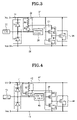
FIG. 3 is a circuit diagram for explaining a electrostatic protection device for a semiconductor device according to a preferred embodiment of the present invention; and
FIG. 4 is a circuit diagram for explaining a electrostatic protection device for a semiconductor device according to another embodiment of the present invention.
DETAILED DESCRIPTION OF THE PREFERRED EMBODIMENTS
Hereinafter, a preferred embodiment of the present invention will be described with reference to the accompanying drawings. In the following description and drawings, the same reference numerals are used to designate the same or similar components, and so repetition of the description on the same or similar components will be omitted.
FIG. 3 is a circuit diagram for explaining an electrostatic protection device for a semiconductor device according to the present invention.
The electrostatic protection device for a semiconductor device according to the present invention includes a delivery module 31, a detection module 32, a driver 33, and a discharge module 34. The delivery module 31 includes diodes D1 and D2 serially connected between a line 37 of an external voltage Vcc and a line 38 of a grounding voltage Vss. Cathodes of the diodes D1 and D2 are connected to the side of the line 37 of the external voltage Vcc, and anodes of the diodes D1 and D2 are connected to the side of the line 38 of the grounding voltage Vss. The delivery module 31 induces static electricity to the line 37 of the external voltage Vcc such that static electricity introduced through an input/output port 35 is not delivered to an internal circuit 36.
The detection module 32 includes a resistor R4 and a diode D3 serially connected between the line 37 of the external voltage Vcc and an input port 35 of the internal circuit 36. The detection module 32 detects static electricity induced to the line 37 of the external voltage Vcc and applies detected voltage to the driver 33 in response to the static electricity. The detected voltage is obtained by performing voltage drop through a resistor R4 with respect to the static electricity induced to the line 37 of the external voltage Vcc. In other words, the detected voltage is voltage of a common connection port of the resistor R4 and the diode D3, and the driver 33 operates based on the detected voltage.
The driver 33 includes a PMOS transistor P2 and an NMOS transistor N3 serially connected between an output port of the detection module 32 and the line 38 of the grounding voltage Vss. In other words, the driver 33 includes a CMOS type buffer unit formed by the PMOS transistor P2 and the NMOS transistor N3. The detected voltage inputted from the detection module 32 is applied to a source port of the PMOS transistor (P2), and the driver 33 is driven by the detected voltage. The detected voltage inputted from the detection module 32 becomes a supply voltage of the CMOS type buffer unit. When the CMOS type buffer operates based on the detected voltage, the static electricity induced to the line 37 of the external voltage Vcc is applied to the input ports of the CMOS type buffer, that is, gate ports of the PMOS transistor P2 and the NMOS transistor N3. Accordingly, the driver 33 operates the discharge module 34.
The discharge module 34 includes an NMOS transistor N4 connected between the line 37 of the external voltage Vcc and the line 38 of the grounding voltage Vss. A drain port of the NMOS transistor N4 is connected to the line 37 of the external voltage Vcc, and the source port of the NMOS transistor N4 is connected to the line 38 of the grounding voltage Vss. If the discharge module 34 is enabled by the driver 33, the NMOS transistor N4 is turned on. Accordingly, static electricity induced to the line 37 of the external voltage Vcc is delivered to the line 38 of the grounding voltage Vss through the NMOS transistor N4. In other words, the static electricity introduced to the input/output port 35 is induced to the line 37 of the external voltage Vcc and then discharged through the line 38 of the grounding voltage Vss. Accordingly, the electrostatic protection device protects the internal circuit 36 of the semiconductor device from static electricity introduced to the input/output port 35.
Such an electrostatic protection device for a semiconductor device according to the present invention induces static electricity introduced to the input/output port 35 to the line 37 of the external voltage Vcc through the delivery module 31. In addition, the electrostatic protection device always detects static electricity induced to the line 37 of the external voltage Vcc through the detection module 32. In addition, the detection module 32 applies a detected voltage to the driver 33 in response to the static electricity, thereby operating the driver 33. Thus, the driver 33 operates in response to static electricity, so that static electricity induced to the line 37 of the external voltage Vcc is delivered to the line 38 of the grounding voltage Vss through the discharge module 34 and discharged. In other words, when static electricity is introduced to the input/output port 35, the electrostatic protection device for the semiconductor device according to the present invention always operates in response to static electricity. In addition, the electrostatic protection device operates during all intervals of the static electricity. Accordingly, the electrostatic protection device for the semiconductor device according to the present invention operates during all intervals including a rising interval of static electricity introduced to the input/output port 35, thereby protecting the internal circuit 36 of the semiconductor device from static electricity.
FIG. 4 is a circuit diagram for explaining an electrostatic protection device for a semiconductor device according to another embodiment of the present invention. Hereinafter, only components different from the components shown in FIG. 3 will be described.
The electrostatic protection device for a semiconductor device according to the present embodiment includes a detection module 42 having a resistor R5 and a diode type transistor T1 differently from the prior embodiment including the detection module 32 having the resistor R4 and the diode D3. In other words, the detection module 42 of the electrostatic protection device for the semiconductor device according to an embodiment of the present invention includes a resistor element R5 and a diode type transistor T1 connected serially between a line 47 of an external voltage Vcc and an input/output port 45 of the internal circuit 46. A source port of the diode type transistor T1 is commonly connected to the resistor R5, a gate port of the transistor T1 is connected to the line 47 of the external voltage Vcc, and a drain port of the transistor T1 is connected to an input port of the internal circuit 46. The detection module 42 detects static electricity induced to the line 47 of the external voltage Vcc and applies the detected static electricity to the driver 43 as a detected voltage by performing voltage drop with respect to the detected static electricity. In other words, the detection module 42 delivers voltage of the common connection port of the diode type transistor T1 and the resistor R5 to the driver 43 as the detected voltage in response to static electricity.
Such an electrostatic protection device for a semiconductor device according to the present embodiment induces static electricity introduced to the input/output port 45 to the line 47 of the external voltage Vcc through the delivery module 41 and always detects the static electricity induced to the line 47 of the external voltage Vcc through the detection module 42. In addition, the detection module 42 applies a detected voltage to the driver 43 in response to static electricity, thereby operating the driver 43. Thus, the driver 43 operates in response to the static electricity, so that static electricity induced to the line 47 of the external voltage Vcc is delivered to the line 48 of the grounding voltage Vss through the discharge module 44 and discharged. In other words, when static electricity is introduced to the input/output port 45, the electrostatic protection device for a semiconductor device according to the present invention always responds to static electricity and operates during all intervals of the static electricity. Accordingly, the electrostatic protection device for a semiconductor device according to the present invention operates during all intervals including a rising interval of the static electricity introduced to the input/output port 45, thereby protecting the internal circuit 46 from static electricity.
The electrostatic protection device according to the present embodiment may be realized to have the same effects as that according to a prior embodiment.
As described above, according to the present invention, static electricity introduced to an input/output port is detected through a detection module, so that the static electricity can be discharged during all intervals for the introduction of the static electricity. Accordingly, it is possible to stably protect an internal circuit of a semiconductor device from static electricity introduced to an input/output port and to prevent any increase in the size of the semiconductor device.
Although a preferred embodiment of the present invention has been described for illustrative purposes, those skilled in the art will appreciate that various modifications, additions and substitutions are possible, without departing from the scope and spirit of the invention as disclosed in the accompanying claims.

Claims (8)

1. An electrostatic protection device for protecting an internal circuit of a semiconductor device from static electricity introduced into an input/output port of the semiconductor device, the electrostatic protection device comprising:
a delivery unit that induces static electricity introduced to the input/output port to a first reference potential voltage line for the semiconductor device;
a detection unit detecting the static electricity induced from the input/output port to the voltage line and outputting a detected voltage obtained by a voltage drip with respect to the static electricity; and
a PMOS transistor coupled in series to an NMOS transistor, wherein the PMOS has its source coupled to said output terminal, its gate coupled to the first reference potential voltage line and its drain is connected to the drain of the NMOS transistor to form commonly-connected drains, the gate of the NMOS transistor is coupled to the first reference potential line and the source of the NMOS transistor is coupled to a second reference potential line for the semiconductor device; and
the commonly connected drains are coupled to and control a third MOS transistor coupled across the first and second reference potential lines and which shunts static electricity to the second reference potential line.
2. The electrostatic protection device as claimed in claim 1, wherein the the first reference potential voltage line is Vcc for the semiconductor device.
3. The electrostatic protection device as claimed in claim 2, wherein the detection unit is configured to cause only positive-going static electricity to be introduced to the first reference potential voltage line.
4. The electrostatic protection device as claimed in claim 1, wherein the detection unit includes a resistor and a diode serially connected to the voltage line and the input/output port.
5. The electrostatic protection device as claimed in claim 4, wherein a cathode of the diode is connected to the resistor, and an anode of the diode is connected to the input/output port.
6. The electrostatic protection device as claimed in claim 4, wherein an output port of the detection unit is connected to a common connection port of the resistor and the diode.
7. The electrostatic protection device as claimed in claim 1, wherein the detection unit includes a diode type transistor and a resistor serially connected to the voltage line and the input/output port.
8. The electrostatic protection device as claimed in claim 7, wherein an output port of the detection unit is connected to a common connection port of the diode type transistor and the resistor.
US11/317,764 2004-12-28 2005-12-23 Electrostatic protection device for semiconductor device Active 2025-12-28 US7286331B2 (en)

Applications Claiming Priority (2)

Application Number Priority Date Filing Date Title
KR1020040114210A KR100587089B1 (en) 2004-12-28 2004-12-28 Electrostatic protection device for semiconductor device
KR10-2004-0114210 2004-12-28

Publications (2)

Publication Number Publication Date
US20060139826A1 US20060139826A1 (en) 2006-06-29
US7286331B2 true US7286331B2 (en) 2007-10-23

Family

ID=36611194

Family Applications (1)

Application Number Title Priority Date Filing Date
US11/317,764 Active 2025-12-28 US7286331B2 (en) 2004-12-28 2005-12-23 Electrostatic protection device for semiconductor device

Country Status (2)

Country Link
US (1) US7286331B2 (en)
KR (1) KR100587089B1 (en)

Cited By (6)

* Cited by examiner, † Cited by third party
Publication number Priority date Publication date Assignee Title
US20060215344A1 (en) * 2005-03-11 2006-09-28 Choi Nak H Electrostatic protection device for semiconductor device
US20080158749A1 (en) * 2005-12-30 2008-07-03 Kwak Kook Whee Electrostatic discharge protection circuit protecting thin gate insulation layers in a semiconductor device
US9219055B2 (en) 2012-06-14 2015-12-22 International Business Machines Corporation Structure and method for dynamic biasing to improve ESD robustness of current mode logic (CML) drivers
US9614368B2 (en) * 2015-02-10 2017-04-04 Texas Instruments Incorporated Area-efficient active-FET ESD protection circuit
US10396550B2 (en) 2016-09-30 2019-08-27 Texas Instruments Incorporated ESD protection charge pump active clamp for low-leakage applications
US10749336B2 (en) 2016-11-28 2020-08-18 Texas Instruments Incorporated ESD protection circuit with passive trigger voltage controlled shut-off

Families Citing this family (2)

* Cited by examiner, † Cited by third party
Publication number Priority date Publication date Assignee Title
KR100898583B1 (en) * 2006-06-30 2009-05-20 주식회사 하이닉스반도체 Electrostatic discharge protection circuit
KR101016957B1 (en) 2007-02-15 2011-02-28 주식회사 하이닉스반도체 Device to Protect Semiconductor Device from Electrostatic Discharge

Citations (5)

* Cited by examiner, † Cited by third party
Publication number Priority date Publication date Assignee Title
US5946177A (en) 1998-08-17 1999-08-31 Motorola, Inc. Circuit for electrostatic discharge protection
US6078487A (en) * 1992-03-31 2000-06-20 Digital Equipment Corporation Electro-static discharge protection device having a modulated control input terminal
US6690561B2 (en) * 2001-09-06 2004-02-10 Faraday Technology Corp. Effective gate-driven or gate-coupled ESD protection circuit
US20050231866A1 (en) * 2004-03-23 2005-10-20 Mergens Markus P J Method and apparatus for protecting a gate oxide using source/bulk pumping
US20060087788A1 (en) * 2004-09-15 2006-04-27 Atmel Nantes Sa Dual-supply electronic circuit with means for protection against breakdowns, and corresponding protection means

Patent Citations (5)

* Cited by examiner, † Cited by third party
Publication number Priority date Publication date Assignee Title
US6078487A (en) * 1992-03-31 2000-06-20 Digital Equipment Corporation Electro-static discharge protection device having a modulated control input terminal
US5946177A (en) 1998-08-17 1999-08-31 Motorola, Inc. Circuit for electrostatic discharge protection
US6690561B2 (en) * 2001-09-06 2004-02-10 Faraday Technology Corp. Effective gate-driven or gate-coupled ESD protection circuit
US20050231866A1 (en) * 2004-03-23 2005-10-20 Mergens Markus P J Method and apparatus for protecting a gate oxide using source/bulk pumping
US20060087788A1 (en) * 2004-09-15 2006-04-27 Atmel Nantes Sa Dual-supply electronic circuit with means for protection against breakdowns, and corresponding protection means

Cited By (12)

* Cited by examiner, † Cited by third party
Publication number Priority date Publication date Assignee Title
US20060215344A1 (en) * 2005-03-11 2006-09-28 Choi Nak H Electrostatic protection device for semiconductor device
US20080158749A1 (en) * 2005-12-30 2008-07-03 Kwak Kook Whee Electrostatic discharge protection circuit protecting thin gate insulation layers in a semiconductor device
US7839613B2 (en) * 2005-12-30 2010-11-23 Hynix Semiconductor Inc. Electrostatic discharge protection circuit protecting thin gate insulation layers in a semiconductor device
US9219055B2 (en) 2012-06-14 2015-12-22 International Business Machines Corporation Structure and method for dynamic biasing to improve ESD robustness of current mode logic (CML) drivers
US9620497B2 (en) 2012-06-14 2017-04-11 International Business Machines Corporation Structure and method for dynamic biasing to improve ESD robustness of current mode logic (CML) drivers
US10181463B2 (en) 2012-06-14 2019-01-15 International Business Machines Corporation Structure and method for dynamic biasing to improve ESD robustness of current mode logic (CML) drivers
US10756078B2 (en) 2012-06-14 2020-08-25 International Business Machines Corporation Structure and method for dynamic biasing to improve ESD robustness of current mode logic (CML) drivers
US9614368B2 (en) * 2015-02-10 2017-04-04 Texas Instruments Incorporated Area-efficient active-FET ESD protection circuit
US10181721B2 (en) 2015-02-10 2019-01-15 Texas Instruments Incorporated Area-efficient active-FET ESD protection circuit
US10396550B2 (en) 2016-09-30 2019-08-27 Texas Instruments Incorporated ESD protection charge pump active clamp for low-leakage applications
US11114848B2 (en) 2016-09-30 2021-09-07 Texas Instruments Incorporated ESD protection charge pump active clamp for low-leakage applications
US10749336B2 (en) 2016-11-28 2020-08-18 Texas Instruments Incorporated ESD protection circuit with passive trigger voltage controlled shut-off

Also Published As

Publication number Publication date
KR100587089B1 (en) 2006-06-08
US20060139826A1 (en) 2006-06-29

Similar Documents

Publication Publication Date Title
US7286331B2 (en) Electrostatic protection device for semiconductor device
KR101110942B1 (en) Electrostatic discharge protection circuit and method of operation
US7839613B2 (en) Electrostatic discharge protection circuit protecting thin gate insulation layers in a semiconductor device
US8520351B2 (en) Electrostatic discharge protective circuit having rise time detector and discharge sustaining circuitry
US20080316660A1 (en) Electrostatic discharge avoiding circuit
KR101039856B1 (en) A circuit for electrostatic to discharge
TW201926837A (en) Electrostatic discharge (ESD) protection circuit and integrated circuit including the same
US20130222954A1 (en) Electrostatic discharge protection circuit
KR20140042466A (en) Clamping circuit, semiconductor having the same and clamping method thereof
US10181721B2 (en) Area-efficient active-FET ESD protection circuit
KR101016964B1 (en) Circuit To Protect Semiconductor Device From Electro Static Discharge
US20070236842A1 (en) Electrostatic discharge protection circuit
US9431823B2 (en) ESD protection circuit
US20090067106A1 (en) Static electricity discharge circuit
US20060268477A1 (en) Apparatus for ESD protection
US7154719B2 (en) Circuit for electrostatic discharge protection
US7675722B2 (en) Device to protect semiconductor device from electrostatic discharge
US7312966B2 (en) Electrostatic discharge protection circuit
US6809915B2 (en) Gate-equivalent-potential circuit and method for I/O ESD protection
US10366979B2 (en) Electrostatic discharge protection circuit and method for electrostatic discharge protection
US20050041346A1 (en) Circuit and method for ESD protection
US6757147B1 (en) Pin-to-pin ESD-protection structure having cross-pin activation
US20210273448A1 (en) Electrical stress protection circuit and electronic device including the same
KR100338105B1 (en) Electro static discharge structure for a semiconductor device
CN101394081A (en) Electro-static discharge protection design with low capacitance

Legal Events

Date Code Title Description
AS Assignment

Owner name: HYNIX SEMICONDUCTOR INC., KOREA, REPUBLIC OF

Free format text: ASSIGNMENT OF ASSIGNORS INTEREST;ASSIGNOR:CHOI, NAK HEON;REEL/FRAME:017415/0276

Effective date: 20051216

STCF Information on status: patent grant

Free format text: PATENTED CASE

FEPP Fee payment procedure

Free format text: PAYOR NUMBER ASSIGNED (ORIGINAL EVENT CODE: ASPN); ENTITY STATUS OF PATENT OWNER: LARGE ENTITY

FEPP Fee payment procedure

Free format text: PAYOR NUMBER ASSIGNED (ORIGINAL EVENT CODE: ASPN); ENTITY STATUS OF PATENT OWNER: LARGE ENTITY

Free format text: PAYER NUMBER DE-ASSIGNED (ORIGINAL EVENT CODE: RMPN); ENTITY STATUS OF PATENT OWNER: LARGE ENTITY

FPAY Fee payment

Year of fee payment: 4

FPAY Fee payment

Year of fee payment: 8

MAFP Maintenance fee payment

Free format text: PAYMENT OF MAINTENANCE FEE, 12TH YEAR, LARGE ENTITY (ORIGINAL EVENT CODE: M1553); ENTITY STATUS OF PATENT OWNER: LARGE ENTITY

Year of fee payment: 12