US7282689B2 - Optical fiber receiver having an increased bandwidth - Google Patents
Optical fiber receiver having an increased bandwidth Download PDFInfo
- Publication number
- US7282689B2 US7282689B2 US10/507,306 US50730605A US7282689B2 US 7282689 B2 US7282689 B2 US 7282689B2 US 50730605 A US50730605 A US 50730605A US 7282689 B2 US7282689 B2 US 7282689B2
- Authority
- US
- United States
- Prior art keywords
- receiver
- fibre
- photo
- optical
- spot
- Prior art date
- Legal status (The legal status is an assumption and is not a legal conclusion. Google has not performed a legal analysis and makes no representation as to the accuracy of the status listed.)
- Expired - Fee Related
Links
Images


Classifications
-
- H—ELECTRICITY
- H04—ELECTRIC COMMUNICATION TECHNIQUE
- H04B—TRANSMISSION
- H04B10/00—Transmission systems employing electromagnetic waves other than radio-waves, e.g. infrared, visible or ultraviolet light, or employing corpuscular radiation, e.g. quantum communication
- H04B10/60—Receivers
-
- H—ELECTRICITY
- H10—SEMICONDUCTOR DEVICES; ELECTRIC SOLID-STATE DEVICES NOT OTHERWISE PROVIDED FOR
- H10F—INORGANIC SEMICONDUCTOR DEVICES SENSITIVE TO INFRARED RADIATION, LIGHT, ELECTROMAGNETIC RADIATION OF SHORTER WAVELENGTH OR CORPUSCULAR RADIATION
- H10F77/00—Constructional details of devices covered by this subclass
- H10F77/10—Semiconductor bodies
- H10F77/14—Shape of semiconductor bodies; Shapes, relative sizes or dispositions of semiconductor regions within semiconductor bodies
- H10F77/148—Shapes of potential barriers
-
- H—ELECTRICITY
- H03—ELECTRONIC CIRCUITRY
- H03F—AMPLIFIERS
- H03F3/00—Amplifiers with only discharge tubes or only semiconductor devices as amplifying elements
- H03F3/04—Amplifiers with only discharge tubes or only semiconductor devices as amplifying elements with semiconductor devices only
- H03F3/08—Amplifiers with only discharge tubes or only semiconductor devices as amplifying elements with semiconductor devices only controlled by light
- H03F3/087—Amplifiers with only discharge tubes or only semiconductor devices as amplifying elements with semiconductor devices only controlled by light with IC amplifier blocks
-
- H—ELECTRICITY
- H04—ELECTRIC COMMUNICATION TECHNIQUE
- H04B—TRANSMISSION
- H04B10/00—Transmission systems employing electromagnetic waves other than radio-waves, e.g. infrared, visible or ultraviolet light, or employing corpuscular radiation, e.g. quantum communication
- H04B10/25—Arrangements specific to fibre transmission
- H04B10/2581—Multimode transmission
-
- H—ELECTRICITY
- H04—ELECTRIC COMMUNICATION TECHNIQUE
- H04B—TRANSMISSION
- H04B10/00—Transmission systems employing electromagnetic waves other than radio-waves, e.g. infrared, visible or ultraviolet light, or employing corpuscular radiation, e.g. quantum communication
- H04B10/60—Receivers
- H04B10/66—Non-coherent receivers, e.g. using direct detection
-
- H—ELECTRICITY
- H10—SEMICONDUCTOR DEVICES; ELECTRIC SOLID-STATE DEVICES NOT OTHERWISE PROVIDED FOR
- H10F—INORGANIC SEMICONDUCTOR DEVICES SENSITIVE TO INFRARED RADIATION, LIGHT, ELECTROMAGNETIC RADIATION OF SHORTER WAVELENGTH OR CORPUSCULAR RADIATION
- H10F39/00—Integrated devices, or assemblies of multiple devices, comprising at least one element covered by group H10F30/00, e.g. radiation detectors comprising photodiode arrays
- H10F39/10—Integrated devices
- H10F39/103—Integrated devices the at least one element covered by H10F30/00 having potential barriers, e.g. integrated devices comprising photodiodes or phototransistors
-
- H—ELECTRICITY
- H10—SEMICONDUCTOR DEVICES; ELECTRIC SOLID-STATE DEVICES NOT OTHERWISE PROVIDED FOR
- H10F—INORGANIC SEMICONDUCTOR DEVICES SENSITIVE TO INFRARED RADIATION, LIGHT, ELECTROMAGNETIC RADIATION OF SHORTER WAVELENGTH OR CORPUSCULAR RADIATION
- H10F77/00—Constructional details of devices covered by this subclass
- H10F77/95—Circuit arrangements
- H10F77/953—Circuit arrangements for devices having potential barriers
-
- H—ELECTRICITY
- H10—SEMICONDUCTOR DEVICES; ELECTRIC SOLID-STATE DEVICES NOT OTHERWISE PROVIDED FOR
- H10F—INORGANIC SEMICONDUCTOR DEVICES SENSITIVE TO INFRARED RADIATION, LIGHT, ELECTROMAGNETIC RADIATION OF SHORTER WAVELENGTH OR CORPUSCULAR RADIATION
- H10F30/00—Individual radiation-sensitive semiconductor devices in which radiation controls the flow of current through the devices, e.g. photodetectors
- H10F30/20—Individual radiation-sensitive semiconductor devices in which radiation controls the flow of current through the devices, e.g. photodetectors the devices having potential barriers, e.g. phototransistors
- H10F30/21—Individual radiation-sensitive semiconductor devices in which radiation controls the flow of current through the devices, e.g. photodetectors the devices having potential barriers, e.g. phototransistors the devices being sensitive to infrared, visible or ultraviolet radiation
- H10F30/22—Individual radiation-sensitive semiconductor devices in which radiation controls the flow of current through the devices, e.g. photodetectors the devices having potential barriers, e.g. phototransistors the devices being sensitive to infrared, visible or ultraviolet radiation the devices having only one potential barrier, e.g. photodiodes
- H10F30/221—Individual radiation-sensitive semiconductor devices in which radiation controls the flow of current through the devices, e.g. photodetectors the devices having potential barriers, e.g. phototransistors the devices being sensitive to infrared, visible or ultraviolet radiation the devices having only one potential barrier, e.g. photodiodes the potential barrier being a PN homojunction
-
- Y—GENERAL TAGGING OF NEW TECHNOLOGICAL DEVELOPMENTS; GENERAL TAGGING OF CROSS-SECTIONAL TECHNOLOGIES SPANNING OVER SEVERAL SECTIONS OF THE IPC; TECHNICAL SUBJECTS COVERED BY FORMER USPC CROSS-REFERENCE ART COLLECTIONS [XRACs] AND DIGESTS
- Y02—TECHNOLOGIES OR APPLICATIONS FOR MITIGATION OR ADAPTATION AGAINST CLIMATE CHANGE
- Y02E—REDUCTION OF GREENHOUSE GAS [GHG] EMISSIONS, RELATED TO ENERGY GENERATION, TRANSMISSION OR DISTRIBUTION
- Y02E10/00—Energy generation through renewable energy sources
- Y02E10/50—Photovoltaic [PV] energy
Definitions
- the invention concerns a (monolithic) integrated optical fibre receiver with an increased sensitivity and increased bandwidth.
- Known optical fibre receivers consist primarily of a photodiode and of a transimpedance amplifier which converts the current from the photodiode into a proportional voltage. See, for instance, DE 32 33 146 (AT&T Technologies) or DE 33 38 024 (SEL AG). A decision circuit may also follow, whose task is to decide whether the light level being received corresponds to a logical zero or to a logical one.
- Optical fibres with larger diameters produce a light spot that is correspondingly large. When, for instance, plastic fibres are used, the spot of light that is to be received can be, relatively, very large (up to one millimetre in diameter).
- the photosensitive surface of the receiving photo diode is correspondingly modified.
- the depletion layer capacitance of a photo diode also rises, resulting in a deterioration both of its speed and of the noise behaviour of the subsequent transimpedance amplifier.
- a technical problem addressed by the invention is that of providing a relatively large light-sensitive receptive area for fast optical signals, and yet to increase the bandwidth and the sensitivity of the optical receiver.
- This challenge is answered, in accordance with the invention, by dividing an optical receiver diode whose size has been adapted to that of the spot of light, and by following each individual partial photodiode with its own transimpedance amplifier.
- the output signals from the individual (separate) transimpedance amplifiers are integrated in a summing amplifier.
- the individual transimpedance amplifiers have a wider bandwidth and a better noise behaviour. These properties are only insignificantly affected by the summing amplifier.
- the principle of division of an optical receiver can also be implemented in bipolar and BICMOS OEICs. Due to the higher level of amplification, these can achieve data rates even higher than 622 Mbit/s with an effective diameter of have 1 mm for a photo diode.
- a further possible application lies with optical receivers for glass fibres or for plastic fibres that permit a high tolerance in the adjustment of plug-in optical connectors, or which do not require adjustment.
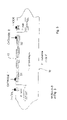
- FIG. 1 shows a view from above of a photodiode in an optical fibre receiver according to the prior art (schematic).
- FIG. 2 shows the circuit of a photodiode with a transimpedance amplifier 29 .
- FIG. 3 shows a view from above of a photodiode in an example of the optical fibre receiver in accordance with the invention (schematic).
- FIG. 4 shows a circuit in accordance with the invention with partial photodiodes and with a number of transimpedance amplifiers and the summing amplifier.
- FIG. 5 is a vertical section through the PIN photodiode according to FIG. 3 (schematic).
- FIG. 6 is a diagram of the input noise density plotted against the frequency.
- the full-area photodiode D in FIG. 1 manufactured in 0.6 pm CMOS technology, has a diameter “dl” of 400 pm and a depletion layer capacitance of about 1.6 pF.
- the four partial photodiodes D 1 , D 2 , D 3 and D 4 in FIG. 3 (each) have a depletion layer capacitance of 400 fF.
- An electrical contact 10 to the photodiodes to the rear of the substrate (see FIG. 5 with section A-B from FIG. 3 ) considerably reduces the series resistance of the PIN diodes.
- the transimpedance amplifiers 20 to 23 in accordance with FIG. 4 have a transimpedance of 70 kOhm, while the summing amplifier 30 has an amplification factor of 2.5.
- the bandwidth of the transimpedance amplifier 29 associated with the full-area photodiode D according to FIGS. 1 and 2 is 151 MHz, while that of the total system involving four divided photodiodes 11 in accordance with FIGS. 3 and 4 having the same receiver area is 402 MHz.
- the transimpedance of the total system with four divided photodiodes in accordance with FIG. 4 is 164 kOhm.
- the electrical circuitry connecting the individual photodiodes D 1 to D 4 can be seen in FIG. 4 .
- One of the amplifiers 20 to 23 is allocated to each of the partial diodes and accepts its electrical output signal. Through a circuit configuration as current-voltage converters with feedback resistance Rf, each of the individual transimpedance amplifiers is responsible for one partial diode.
- the output signals are not illustrated separately, but are present at the input resistor R 1 of the summing circuit 30 , which, through its feedback resistor R 2 , determines the amplification factor of the summing circuit. In the illustration above, this has been selected to be 2.5.
- the structure of the individual diodes in accordance with FIG. 3 can be seen in the sectional diagram of FIG. 5 .
- the two photodiodes D 1 and D 2 seen through section A-B appear as Photodiode 1 and Photodiode 2 , and their N+ regions are separated by a narrow strip 12 .
- This cathode region is unique for each photodiode, and is connected to the associated amplifier in accordance with FIG. 4 .
- the relevant anode connection of a partial diode is made to the P+ region above the P well and the buried P+ layer in the epitaxial layer, and on the both sides of the N+ layer of each photodiode D 1 and D 2 .
- the anodes can be connected to ground.
- FIG. 5 is only a section of an integrated circuit which can extend further to the left and to the right, in particular including integrated circuit amplifiers as they are indicated on FIG. 4 , or also further optical fibre receivers.
- Each optical fibre receiver here is coupled through an electrical plug-in connector to an optical fibre—not shown—in order to project a light spot from the optical fibre onto the optical fibre receiver of FIG. 3 .
- the size of the spot of light can be seen in the sectional view for the two partial diodes D 1 and D 2 .
- FIG. 1 and FIG. 2 show in FIG. 1 and FIG. 2 a form having a number of corners which approximates largely to a circular shape but which recognises aspects of production technology relevant to optimised manufacture in integrated form.
- the anode terminals of the diodes are joined to a common potential.
- the cathode terminals of the diodes are each independently connected to one input of the transimpedance amplifiers that electrically convert or amplify the signals, in preparation for subsequent electrical combination in the summing circuit 30 .
- no highly electrically conductive connection is provided between anode and cathode 1 or between anode and cathode 2 of the two photodiodes D 1 and D 2 , which means that the two connections are not joined by an electrically conductive coupling. This only changes for one of the connections of each diode after they are configured in accordance with FIG. 4 .
- FIG. 6 compares the equivalent input noise densities of the following systems:
- the input noise densities are integrated over the range 1 MHz to 150 MHz, the following values are obtained for the equivalent input noise densities: for the full-area photodiode with one transimpedance amplifier we obtain 59.3 nA, while for the four divided photo diodes 11 with four transimpedance amplifiers and a summing amplifier, the figure is 33.5 nA.
- the bandwidth can be more than doubled, while the equivalent input noise current with constant bandwidth can be almost halved.
- the bandwidth of the whole system 402 MHz, is enough to process a non-return-to-zero (NRZ) data rate of 500 Mbit/s or of 622 Mbit/s.
- NZ non-return-to-zero
- the depletion layer capacitance is 8.8 pF.
- One of the four partial photo diodes therefore has a depletion layer capacitance of 2.2 pF.
- a further possible application lies with optical receivers for glass fibres or for plastic fibres that permit a high tolerance in the adjustment of plug-in optical connectors, or which do not require adjustment.
Landscapes
- Engineering & Computer Science (AREA)
- Physics & Mathematics (AREA)
- Electromagnetism (AREA)
- Computer Networks & Wireless Communication (AREA)
- Signal Processing (AREA)
- Power Engineering (AREA)
- Amplifiers (AREA)
- Light Receiving Elements (AREA)
- Optical Communication System (AREA)
- Manufacture, Treatment Of Glass Fibers (AREA)
- Artificial Filaments (AREA)
- Addition Polymer Or Copolymer, Post-Treatments, Or Chemical Modifications (AREA)
- Optical Couplings Of Light Guides (AREA)
- Solid State Image Pick-Up Elements (AREA)
- Glass Compositions (AREA)
Abstract
The invention relates to an optical fiber receiver (11) for optoelectronic integrated circuits (OEIC's) having an improved sensitivity and improved bandwidth. The improvements are achieved by subdividing the photodiodes into partial photodiodes (D1, D2), whereby each partial photodiode is connected to a respective transimpedance amplifier (20, 21), and the output signals of the individual transimpedance amplifiers are added inside a summation amplifier (30). The optical fiber received can be produced using different technologies: CMOS, BICMOS, BIPOLAR.
Description
The invention concerns a (monolithic) integrated optical fibre receiver with an increased sensitivity and increased bandwidth.
Known optical fibre receivers consist primarily of a photodiode and of a transimpedance amplifier which converts the current from the photodiode into a proportional voltage. See, for instance, DE 32 33 146 (AT&T Technologies) or DE 33 38 024 (SEL AG). A decision circuit may also follow, whose task is to decide whether the light level being received corresponds to a logical zero or to a logical one. Optical fibres with larger diameters produce a light spot that is correspondingly large. When, for instance, plastic fibres are used, the spot of light that is to be received can be, relatively, very large (up to one millimetre in diameter). In order to be able to fully exploit the incoming light flux, the photosensitive surface of the receiving photo diode is correspondingly modified. However, with the increase in receptive area, the depletion layer capacitance of a photo diode also rises, resulting in a deterioration both of its speed and of the noise behaviour of the subsequent transimpedance amplifier.
A technical problem addressed by the invention is that of providing a relatively large light-sensitive receptive area for fast optical signals, and yet to increase the bandwidth and the sensitivity of the optical receiver.
This challenge is answered, in accordance with the invention, by dividing an optical receiver diode whose size has been adapted to that of the spot of light, and by following each individual partial photodiode with its own transimpedance amplifier. The output signals from the individual (separate) transimpedance amplifiers are integrated in a summing amplifier.
Because the partial photodiodes have a lower depletion layer capacitance than a larger diode whose area corresponds to the total, the individual transimpedance amplifiers have a wider bandwidth and a better noise behaviour. These properties are only insignificantly affected by the summing amplifier.
The principle of division of an optical receiver can also be implemented in bipolar and BICMOS OEICs. Due to the higher level of amplification, these can achieve data rates even higher than 622 Mbit/s with an effective diameter of have 1 mm for a photo diode.
These high data rates can for the first time be achieved with the aid of the photodiode division principle, in combination with an effective photodiode diameter of up to 1 mm. In this way an optoelectronic integrated circuit (OEIC) for a plastic fibre with a diameter of around 1 mm can achieve a data rate of more than 500 Mbit/s.
A further possible application lies with optical receivers for glass fibres or for plastic fibres that permit a high tolerance in the adjustment of plug-in optical connectors, or which do not require adjustment.
The invention will be explained with the aid of example implementations. All the elements illustrated should be a understood as having been manufactured by integrating them onto one chip in CMOS technology, unless described otherwise.
The full-area photodiode D in FIG. 1 , manufactured in 0.6 pm CMOS technology, has a diameter “dl” of 400 pm and a depletion layer capacitance of about 1.6 pF. The four partial photodiodes D1, D2, D3 and D4 in FIG. 3 (each) have a depletion layer capacitance of 400 fF. An electrical contact 10 to the photodiodes to the rear of the substrate (see FIG. 5 with section A-B from FIG. 3 ) considerably reduces the series resistance of the PIN diodes.
The transimpedance amplifiers 20 to 23 in accordance with FIG. 4 have a transimpedance of 70 kOhm, while the summing amplifier 30 has an amplification factor of 2.5. The bandwidth of the transimpedance amplifier 29 associated with the full-area photodiode D according to FIGS. 1 and 2 is 151 MHz, while that of the total system involving four divided photodiodes 11 in accordance with FIGS. 3 and 4 having the same receiver area is 402 MHz.
The transimpedance of the total system with four divided photodiodes in accordance with FIG. 4 is 164 kOhm.
The electrical circuitry connecting the individual photodiodes D1 to D4 can be seen in FIG. 4 . One of the amplifiers 20 to 23 is allocated to each of the partial diodes and accepts its electrical output signal. Through a circuit configuration as current-voltage converters with feedback resistance Rf, each of the individual transimpedance amplifiers is responsible for one partial diode. The output signals are not illustrated separately, but are present at the input resistor R1 of the summing circuit 30, which, through its feedback resistor R2, determines the amplification factor of the summing circuit. In the illustration above, this has been selected to be 2.5.
The structure of the individual diodes in accordance with FIG. 3 can be seen in the sectional diagram of FIG. 5 . The two photodiodes D1 and D2 seen through section A-B appear as Photodiode 1 and Photodiode 2, and their N+ regions are separated by a narrow strip 12. This cathode region is unique for each photodiode, and is connected to the associated amplifier in accordance with FIG. 4 . The relevant anode connection of a partial diode is made to the P+ region above the P well and the buried P+ layer in the epitaxial layer, and on the both sides of the N+ layer of each photodiode D1 and D2. The anodes can be connected to ground.
A further anode 10 on the rear of the substrate can significantly reduce the series resistance of the diodes. FIG. 5 is only a section of an integrated circuit which can extend further to the left and to the right, in particular including integrated circuit amplifiers as they are indicated on FIG. 4 , or also further optical fibre receivers. Each optical fibre receiver here is coupled through an electrical plug-in connector to an optical fibre—not shown—in order to project a light spot from the optical fibre onto the optical fibre receiver of FIG. 3 . The size of the spot of light can be seen in the sectional view for the two partial diodes D1 and D2.
It should of course be clear that the figure given for the diameter is an approximate value, and that it does not necessarily have a circular shape, as its name suggests. The corresponding diagram shows in FIG. 1 and FIG. 2 a form having a number of corners which approximates largely to a circular shape but which recognises aspects of production technology relevant to optimised manufacture in integrated form.
After connecting the individual diodes D1 to D4 to their corresponding transimpedance amplifiers 20 to 23, the anode terminals of the diodes are joined to a common potential. The cathode terminals of the diodes are each independently connected to one input of the transimpedance amplifiers that electrically convert or amplify the signals, in preparation for subsequent electrical combination in the summing circuit 30. On the basis of FIG. 5 , no highly electrically conductive connection is provided between anode and cathode 1 or between anode and cathode 2 of the two photodiodes D1 and D2, which means that the two connections are not joined by an electrically conductive coupling. This only changes for one of the connections of each diode after they are configured in accordance with FIG. 4 .
(a) a full-area photodiode D with one transimpedance amplifier;
(b) a partial photodiode D1 with one transimpedance amplifier and
(c) four partial photo diodes, each having its own transimpedance amplifier followed by addition in summing amplifier 30.
If the input noise densities are integrated over the range 1 MHz to 150 MHz, the following values are obtained for the equivalent input noise densities: for the full-area photodiode with one transimpedance amplifier we obtain 59.3 nA, while for the four divided photo diodes 11 with four transimpedance amplifiers and a summing amplifier, the figure is 33.5 nA.
By dividing the four photodiodes, the bandwidth can be more than doubled, while the equivalent input noise current with constant bandwidth can be almost halved.
The bandwidth of the whole system, 402 MHz, is enough to process a non-return-to-zero (NRZ) data rate of 500 Mbit/s or of 622 Mbit/s.
For a photodiode with a diameter “d2” of 1 mm, the depletion layer capacitance is 8.8 pF. One of the four partial photo diodes therefore has a depletion layer capacitance of 2.2 pF. For the four equally divided photo diodes, we reach with a transimpedance of 164 kOhm a bandwidth of 116 MHz, which is sufficient for a data rate of 155 Mbit/s. If the feedback resistor Rf in the amplifiers 20 to 23 is reduced, then at a transimpedance of 32.6 kOhm a bandwidth of 413 MHz (corresponding to a data rate of 622 Mbit/s) is achieved.
These data rates can for the first time be achieved with the aid of the photodiode principle, in combination with an effective photodiode diameter of 1 mm. In this way an optoelectronic integrated circuit (OEIC) for a plastic fibre with a diameter of 1 mm can achieve a data rate of more than 500 Mbit/s.
A further possible application lies with optical receivers for glass fibres or for plastic fibres that permit a high tolerance in the adjustment of plug-in optical connectors, or which do not require adjustment.
Claims (14)
1. An optical fibre receiver for an opto-electronic integrated circuit (OEIC), comprising at least one photo-receiver (11) and at least one transimpedance amplifier, wherein
(i) the photo-receiver (11) is divided into several partial photo-diodes (D1, D2, D3, D4) in order to consist of a number of individual photo-diodes, wherein the size of the partial photo-diodes is adapted to that of a spot of light projected onto the photo-receiver (11);
(ii) each partial photo-diode (D1, D2, D3, D4) is connected to an own transimpedance amplifier (20, 21, 22, 23), and the electrical output signals of the transimpedanee amplifiers (20, 21, 22, 23) are combined electrically by a summing amplifier (30); and
(iii) wherein at least the photo-receiver (11), the transimpedance amplifiers and the summing amplifier (30) are monolithic integrated onto a chip together with other circuit components.
2. The fibre receiver according to claim 1 , wherein the receiver is manufactured in a CMOS technology.
3. The fibre receiver according to claim 1 , wherein the receiver is manufactured in a bipolar technology.
4. The fibre receiver according to claim 1 , wherein the receiver is manufactured in a BiCMOS technology.
5. The fibre receiver according to one of the preceding claims, wherein the receiver, which is an integrated component of the monolithic circuit, comprising the photo-receiver (11) having a size up to substantially 1 mm diameter (d2).
6. The fibre receiver according to claim 1 , wherein the transimpedance amplifiers (20, 21, 22, 23) are provided as operational amplifier circuits.
7. The fibre receiver according to one of the claims 1 or 6 , wherein the transimpedance amplifiers (20, 21, 22, 23) are wired as current-voltage converters.
8. The fibre receiver according to claim 1 , wherein four partial regions (D1, D2, D3, D4) of the photo-receiver (11) are provided as separate photo-diodes having between each other an optically or electrically insensitive intermediate zone (12).
9. A method for receiving a high frequency light signal in an optical receiver (11) at an end of an optical fibre, wherein a spot of light projected by the fibre onto the optical receiver (11) falls on several individual regions (D1, D2, D3, D4) of the optical receiver (11), these regions being electrically decoupled from each other or having no essential electrical conductance to each other, wherein the size of the several individual regions is adapted to that of the spot of light, or vice versa, and wherein each electrical signal provided by each individual region is connected to an independent, high-bandwidth amplifier (20, 21, 22, 23), thereafter they are electrically combined (30).
10. The method according to claim 9 , wherein the optical receiver (11) converts substantially concurrently an optical signal from the same fibre into several corresponding electrical signals by several independent photo-diodes acting as individual regions.
11. The method according to claim 9 , wherein the optical fibre is a relatively thick plastic fibre.
12. The method according to one of the claims 9 or 11 , wherein the spot of light is of an order of magnitude of substantially 1 mm diameter or less, but of a relatively large area.
13. The method according to one of the claims 9 , 12 or 11 wherein each individual region (D1, D2, D3, D4) of the optical receiver (11) is smaller than the spot of light or than a total area of the optical receiver (11) at the end of the optical fibre.
14. The method according to claims 12 , wherein each individual region (D1, D2, D3, D4) of the optical receiver (11) is smaller than the spot of light or than a total area of the optical receiver (11) at the end of the optical fibre.
Applications Claiming Priority (3)
| Application Number | Priority Date | Filing Date | Title |
|---|---|---|---|
| DE10213045A DE10213045B4 (en) | 2002-03-22 | 2002-03-22 | Integrated optical fiber receiver |
| DE10213045.0 | 2002-03-22 | ||
| PCT/DE2003/000969 WO2003081813A2 (en) | 2002-03-22 | 2003-03-24 | Optical fiber receiver having an increased bandwidth |
Publications (2)
| Publication Number | Publication Date |
|---|---|
| US20060163452A1 US20060163452A1 (en) | 2006-07-27 |
| US7282689B2 true US7282689B2 (en) | 2007-10-16 |
Family
ID=28050782
Family Applications (1)
| Application Number | Title | Priority Date | Filing Date |
|---|---|---|---|
| US10/507,306 Expired - Fee Related US7282689B2 (en) | 2002-03-22 | 2003-03-24 | Optical fiber receiver having an increased bandwidth |
Country Status (9)
| Country | Link |
|---|---|
| US (1) | US7282689B2 (en) |
| EP (1) | EP1488549B1 (en) |
| JP (1) | JP2005531129A (en) |
| KR (1) | KR100958218B1 (en) |
| AT (1) | ATE313177T1 (en) |
| AU (1) | AU2003232583A1 (en) |
| DE (3) | DE10213045B4 (en) |
| ES (1) | ES2254955T3 (en) |
| WO (1) | WO2003081813A2 (en) |
Cited By (2)
| Publication number | Priority date | Publication date | Assignee | Title |
|---|---|---|---|---|
| US20210184634A1 (en) * | 2019-12-12 | 2021-06-17 | Applied Materials Israel Ltd. | Detection circuit and method for amplifying a photosensor output current |
| US20220393759A1 (en) * | 2019-10-31 | 2022-12-08 | Technische Universiteit Eindhoven | An optical wireless communication receiver with large photodetector suface area, large field of view and high bandwidth |
Families Citing this family (4)
| Publication number | Priority date | Publication date | Assignee | Title |
|---|---|---|---|---|
| US7230227B2 (en) * | 2004-10-08 | 2007-06-12 | The Boeing Company | Lenslet/detector array assembly for high data rate optical communications |
| EP2216815B1 (en) * | 2009-02-05 | 2014-04-02 | ams AG | Integrated circuit comprising PIN diodes |
| DE102010038479B4 (en) * | 2010-07-27 | 2018-01-04 | Universität Duisburg-Essen | Transmission device for free space transmission of optical signals and associated use |
| US8977139B2 (en) * | 2012-10-29 | 2015-03-10 | Finisar Corporation | Integrated circuits in optical receivers |
Citations (6)
| Publication number | Priority date | Publication date | Assignee | Title |
|---|---|---|---|---|
| US5371623A (en) * | 1992-07-01 | 1994-12-06 | Motorola, Inc. | High bit rate infrared communication system for overcoming multipath |
| JPH1038683A (en) | 1996-07-22 | 1998-02-13 | Nikon Corp | Light intensity detector |
| JPH10164624A (en) | 1996-11-29 | 1998-06-19 | Sony Corp | White balance measurement device |
| US5790295A (en) * | 1995-08-28 | 1998-08-04 | Apple Computer, Inc. | Gated integrator preamplifier for infrared data networks |
| US20020003649A1 (en) | 2000-06-13 | 2002-01-10 | Feng Kai D. | Parallel opto-electric structure for high sensitivity and wide bandwidth optical transceiver |
| US6392219B1 (en) * | 2000-03-06 | 2002-05-21 | Tektronix, Inc. | Discrete filter-less optical reference receiver and output amplifier |
Family Cites Families (7)
| Publication number | Priority date | Publication date | Assignee | Title |
|---|---|---|---|---|
| US4540952A (en) * | 1981-09-08 | 1985-09-10 | At&T Bell Laboratories | Nonintegrating receiver |
| DE3338024A1 (en) * | 1983-10-20 | 1985-05-02 | Standard Elektrik Lorenz Ag, 7000 Stuttgart | AMPLIFIER WITH CURRENT-VOLTAGE CONVERSION, IN PARTICULAR PRE-AMPLIFIER OF AN OPTICAL RECEIVER |
| US5235672A (en) * | 1991-02-06 | 1993-08-10 | Irvine Sensors Corporation | Hardware for electronic neural network |
| JPH0837501A (en) * | 1994-07-25 | 1996-02-06 | Ricoh Co Ltd | Optical receiver |
| JPH1146010A (en) * | 1997-05-27 | 1999-02-16 | Hamamatsu Photonics Kk | Avalanche photodiode |
| JPH11340925A (en) * | 1998-05-28 | 1999-12-10 | Sanyo Electric Co Ltd | Semiconductor integrated circuit for receiving light |
| JP4459472B2 (en) * | 2001-04-11 | 2010-04-28 | 浜松ホトニクス株式会社 | Photodetector |
-
2002
- 2002-03-22 DE DE10213045A patent/DE10213045B4/en not_active Expired - Fee Related
-
2003
- 2003-03-24 AT AT03744765T patent/ATE313177T1/en active
- 2003-03-24 ES ES03744765T patent/ES2254955T3/en not_active Expired - Lifetime
- 2003-03-24 KR KR1020047014405A patent/KR100958218B1/en not_active Expired - Fee Related
- 2003-03-24 AU AU2003232583A patent/AU2003232583A1/en not_active Abandoned
- 2003-03-24 WO PCT/DE2003/000969 patent/WO2003081813A2/en not_active Ceased
- 2003-03-24 JP JP2003579392A patent/JP2005531129A/en active Pending
- 2003-03-24 DE DE50301928T patent/DE50301928D1/en not_active Expired - Lifetime
- 2003-03-24 US US10/507,306 patent/US7282689B2/en not_active Expired - Fee Related
- 2003-03-24 EP EP03744765A patent/EP1488549B1/en not_active Expired - Lifetime
- 2003-03-24 DE DE10391783T patent/DE10391783D2/en not_active Withdrawn - After Issue
Patent Citations (7)
| Publication number | Priority date | Publication date | Assignee | Title |
|---|---|---|---|---|
| US5371623A (en) * | 1992-07-01 | 1994-12-06 | Motorola, Inc. | High bit rate infrared communication system for overcoming multipath |
| US5790295A (en) * | 1995-08-28 | 1998-08-04 | Apple Computer, Inc. | Gated integrator preamplifier for infrared data networks |
| JPH1038683A (en) | 1996-07-22 | 1998-02-13 | Nikon Corp | Light intensity detector |
| JPH10164624A (en) | 1996-11-29 | 1998-06-19 | Sony Corp | White balance measurement device |
| US6392219B1 (en) * | 2000-03-06 | 2002-05-21 | Tektronix, Inc. | Discrete filter-less optical reference receiver and output amplifier |
| US20020003649A1 (en) | 2000-06-13 | 2002-01-10 | Feng Kai D. | Parallel opto-electric structure for high sensitivity and wide bandwidth optical transceiver |
| US6834165B2 (en) * | 2000-06-13 | 2004-12-21 | International Business Machines Corporation | Parallel opto-electric structure for high sensitivity and wide bandwidth optical transceiver |
Non-Patent Citations (1)
| Title |
|---|
| H. Zimmermann, Monolithic Bipolar-, CMOS-, and BiCMOS-Receiver OEICs; CAS '96 Proceedings, vol. 1, 1996 International Semiconductor Conference, Oct. 9-12, 1996, Sinaia, Romania IEEE. |
Cited By (6)
| Publication number | Priority date | Publication date | Assignee | Title |
|---|---|---|---|---|
| US20220393759A1 (en) * | 2019-10-31 | 2022-12-08 | Technische Universiteit Eindhoven | An optical wireless communication receiver with large photodetector suface area, large field of view and high bandwidth |
| US11923900B2 (en) * | 2019-10-31 | 2024-03-05 | Technische Universiteit Eindhoven | Optical wireless communication receiver with large photodetector surface area, large field of view and high bandwidth |
| US20210184634A1 (en) * | 2019-12-12 | 2021-06-17 | Applied Materials Israel Ltd. | Detection circuit and method for amplifying a photosensor output current |
| CN112986649A (en) * | 2019-12-12 | 2021-06-18 | 应用材料以色列公司 | Detection circuit and method for amplifying output current of photoelectric sensor |
| US11177775B2 (en) * | 2019-12-12 | 2021-11-16 | Applied Materials Israel Ltd. | Detection circuit and method for amplifying a photosensor output current |
| TWI780539B (en) * | 2019-12-12 | 2022-10-11 | 以色列商應用材料以色列公司 | Detection circuit and method for amplifying a photosensor output current |
Also Published As
| Publication number | Publication date |
|---|---|
| KR100958218B1 (en) | 2010-05-18 |
| JP2005531129A (en) | 2005-10-13 |
| ES2254955T3 (en) | 2006-06-16 |
| KR20040099325A (en) | 2004-11-26 |
| EP1488549A2 (en) | 2004-12-22 |
| DE10213045A1 (en) | 2003-10-16 |
| WO2003081813A2 (en) | 2003-10-02 |
| DE50301928D1 (en) | 2006-01-19 |
| ATE313177T1 (en) | 2005-12-15 |
| US20060163452A1 (en) | 2006-07-27 |
| DE10391783D2 (en) | 2005-02-10 |
| EP1488549B1 (en) | 2005-12-14 |
| WO2003081813A3 (en) | 2003-11-13 |
| AU2003232583A1 (en) | 2003-10-08 |
| DE10213045B4 (en) | 2004-05-06 |
Similar Documents
| Publication | Publication Date | Title |
|---|---|---|
| US11695378B2 (en) | Optical differential low-noise receivers and related methods | |
| US6574022B2 (en) | Integral differential optical signal receiver | |
| US5130762A (en) | Integrated quantum well feedback structure | |
| US10571639B2 (en) | Optical module | |
| Chen et al. | A 2.5 Gbps CMOS fully integrated optical receicer with lateral PIN detector | |
| CN110830113B (en) | Standard CMOS fully-differential photoelectric integrated receiver for visible light communication | |
| Zimmermann | APD and SPAD receivers | |
| US7282689B2 (en) | Optical fiber receiver having an increased bandwidth | |
| Koonen et al. | Optical wireless GbE receiver with large field-of-view | |
| GB2565199A (en) | Optical detector | |
| US4916305A (en) | Optical detectors with selective bias voltage application | |
| US20060108657A1 (en) | Photodiode detector | |
| US11239805B2 (en) | Differential opto isolator | |
| Chang et al. | A novel electronically switched four-channel receiver using InAlAs-InGaAs MSM-HEMT technology for wavelength-division-multiplexing | |
| Takahata et al. | 10-Gb/s two-channel monolithic photoreceiver array using waveguide pin PDs and HEMTs | |
| US5942749A (en) | Photodetector having means for processing optical input signals | |
| US6952297B2 (en) | Method of differentially connecting photonic devices | |
| US5075794A (en) | Reflective opitical feedback element | |
| Akahori et al. | A 622 Mb/s monolithically integrated InGaAs-InP high-sensitivity transimpedance photoreceiver and a multichannel receiver array | |
| CN115173956B (en) | Photoelectric detection receiver | |
| Youn et al. | A 12.5-Gb/s SiGe BiCMOS optical receiver with a monolithically integrated 850-nm avalanche photodetector | |
| JPH05235397A (en) | Optical receiver | |
| Swoboda et al. | A 2.4 GHz-bandwidth OEIC with voltage-up-converter [optical receiver] | |
| GB2565201A (en) | Concentrator height reduction | |
| Swoboda et al. | A low-noise 1.8 Gbps bipolar OEIC |
Legal Events
| Date | Code | Title | Description |
|---|---|---|---|
| AS | Assignment |
Owner name: MELEXIS GMBH, GERMANY Free format text: ASSIGNMENT OF ASSIGNORS INTEREST;ASSIGNORS:ZIMMERMAN, HORST;FOERTSCH, MICHAEL;PLESS, HOLGER;REEL/FRAME:016437/0935;SIGNING DATES FROM 20041001 TO 20041013 |
|
| CC | Certificate of correction | ||
| FPAY | Fee payment |
Year of fee payment: 4 |
|
| REMI | Maintenance fee reminder mailed | ||
| LAPS | Lapse for failure to pay maintenance fees | ||
| STCH | Information on status: patent discontinuation |
Free format text: PATENT EXPIRED DUE TO NONPAYMENT OF MAINTENANCE FEES UNDER 37 CFR 1.362 |
|
| STCH | Information on status: patent discontinuation |
Free format text: PATENT EXPIRED DUE TO NONPAYMENT OF MAINTENANCE FEES UNDER 37 CFR 1.362 |
|
| FP | Lapsed due to failure to pay maintenance fee |
Effective date: 20151016 |