US7274584B2 - Semiconductor memory device having wordline enable signal line and method of arranging the same - Google Patents
Semiconductor memory device having wordline enable signal line and method of arranging the same Download PDFInfo
- Publication number
- US7274584B2 US7274584B2 US11/330,819 US33081906A US7274584B2 US 7274584 B2 US7274584 B2 US 7274584B2 US 33081906 A US33081906 A US 33081906A US 7274584 B2 US7274584 B2 US 7274584B2
- Authority
- US
- United States
- Prior art keywords
- wordline
- enable signal
- wordline enable
- driver
- sub
- Prior art date
- Legal status (The legal status is an assumption and is not a legal conclusion. Google has not performed a legal analysis and makes no representation as to the accuracy of the status listed.)
- Expired - Fee Related
Links
Images


Classifications
-
- A—HUMAN NECESSITIES
- A01—AGRICULTURE; FORESTRY; ANIMAL HUSBANDRY; HUNTING; TRAPPING; FISHING
- A01K—ANIMAL HUSBANDRY; AVICULTURE; APICULTURE; PISCICULTURE; FISHING; REARING OR BREEDING ANIMALS, NOT OTHERWISE PROVIDED FOR; NEW BREEDS OF ANIMALS
- A01K97/00—Accessories for angling
- A01K97/10—Supports for rods
-
- G—PHYSICS
- G11—INFORMATION STORAGE
- G11C—STATIC STORES
- G11C8/00—Arrangements for selecting an address in a digital store
- G11C8/08—Word line control circuits, e.g. drivers, boosters, pull-up circuits, pull-down circuits, precharging circuits, for word lines
-
- Y—GENERAL TAGGING OF NEW TECHNOLOGICAL DEVELOPMENTS; GENERAL TAGGING OF CROSS-SECTIONAL TECHNOLOGIES SPANNING OVER SEVERAL SECTIONS OF THE IPC; TECHNICAL SUBJECTS COVERED BY FORMER USPC CROSS-REFERENCE ART COLLECTIONS [XRACs] AND DIGESTS
- Y10—TECHNICAL SUBJECTS COVERED BY FORMER USPC
- Y10S—TECHNICAL SUBJECTS COVERED BY FORMER USPC CROSS-REFERENCE ART COLLECTIONS [XRACs] AND DIGESTS
- Y10S81/00—Tools
- Y10S81/01—Tool-support adjuncts
Definitions
- the present invention relates to a semiconductor memory device, and more particularly, to a wordline enable signal line arrangement scheme and a method of arranging wordline enable signal lines.
- a hierarchical divided wordline scheme is increasingly used.
- a wordline is divided into a plurality of sub-wordlines, each having a predetermined length, and the sub-wordlines are driven using a row decoder and a sub-wordline driver.
- the sub-wordline driver is controlled using a main wordline signal output from a main wordline driver and a wordline enable signal output from a wordline enable driver.
- FIG. 1 is a diagram illustrating the selection and arrangement of wordlines in a conventional semiconductor memory device.
- a plurality of memory cell arrays 101 through 109 are arranged in vertical and horizontal directions.
- Wordline enable drivers (PXi Driver) 110 and 111 are arranged in a conjunction zone of a memory core region.
- the wordline enable drivers 110 and 111 use a high voltage, i.e., a VPP voltage, as a power supply voltage and drive their output signals with a VPP voltage.
- a sub-wordline driver (SWD) 112 is arranged between a pair of vertically adjacent memory cell arrays, e.g., between the memory cell arrays 105 and 108 .
- the sub-wordline driver 112 drives a sub-wordline (not shown) in response to a signal input thereto via a main wordline NWE and the output signals of the wordline enable driver 110 .
- the wordline enable drivers 110 and 111 are alternately arranged in the conventional semiconductor memory device, and wordline enable signal lines PXi ⁇ 1 , 3 > and PXi ⁇ 0 , 2 > of the wordline enable drivers 110 and 111 , respectively, vertically extend and branch off in two opposite horizontal directions forming a T shape. Accordingly, the wordline enable signal lines PXi ⁇ 1 , 3 > and PXi ⁇ 0 , 2 > are long and have a large load. Thus, the wordline enable drivers 110 and 111 consume a considerable amount of power, and the speed of driving the sub-wordline is likely to decrease.
- the present invention provides a semiconductor memory device having a wordline enable signal line arrangement scheme which can reduce VPP power consumption and can increase the speed of driving a sub-wordline.
- the present invention also provides a method of arranging wordline enable signal lines in the semiconductor memory device which can reduce VPP power consumption and can increase the speed of driving a sub-wordline.
- a semiconductor memory device includes: an array region, which comprises a plurality of memory cell arrays arranged in vertical and horizontal directions; a wordline enable driver, which generates a plurality of wordline enable signals in response to a plurality of address signals and outputs the wordline enable signals to wordline enable signal lines; and sub-wordline drivers, which drive a sub-wordline in response to a signal input thereto via a main wordline and a wordline enable signal input thereto via the respective wordline enable signal lines.
- the wordline enable signal lines vertically and then horizontally extend and are connected to the respective sub-wordline drivers.
- FIG. 1 is a diagram illustrating the selection and arrangement of wordlines in a conventional semiconductor memory device
- FIG. 2 is a diagram illustrating a wordline enable signal line arrangement scheme of a semiconductor memory device according to an embodiment of the present invention
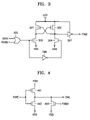
- FIG. 3 is a circuit diagram of an example of a wordline enable driver of FIG. 2 ;
- FIG. 4 is a circuit diagram of an example of a sub-wordline driver of FIG. 2 .
- FIG. 2 is a diagram illustrating a wordline enable signal line arrangement scheme of a semiconductor memory device according to an embodiment of the present invention.
- the semiconductor memory device adopts a method of arranging wordline enable signal lines according to an embodiment of the present invention.
- a plurality of memory cell arrays 201 through 209 are vertically and horizontally arranged in an array region 200 .
- Wordline enable drivers (PXi/PXiB DRIVER) 211 and 212 are arranged in a row decoder region 300 , which may be located outside of the array region 200 .
- the wordline enable driver 211 generates a plurality of wordline enable signals in response to a plurality of address signals RA 0 B 1 B, RA 01 B, RA 0 B 1 , RA 01 and RA 8 B and outputs the wordline enable signals to the respective wordline enable signal lines PXi ⁇ 0 - 3 >.
- the wordline enable driver 212 generates a plurality of wordline enable signals in response to the address signals RA 0 B 1 B, RA 01 B, RA 0 B 1 and RA 01 and an address signal RA 8 and outputs the wordline enable signals to the respective wordline enable signal lines PXi ⁇ 0 - 3 >.
- the wordline enable drivers 211 and 212 are selected in response to the address signals RA 8 B and RA 8 , respectively.
- the semiconductor memory device is manufactured using three metal layers, and the wordline enable signal lines PXi ⁇ 0 - 3 > are formed from one of the three metal layers, and in this embodiment illustrated in FIG. 2 , from the uppermost metal layer.
- Sub-wordline drivers (SWD) 210 are arranged between a pair of vertically adjacent memory cell arrays, for example, between the memory cell arrays 205 and 208 .
- Each of the sub-wordline drivers 210 drives a sub-wordline (not shown) in response to a signal input thereto via a main wordline NWE and a wordline enable signal input thereto via a corresponding wordline enable signal line PXi ⁇ 0 - 3 >.
- the wordline enable drivers 211 and 212 are arranged in the row decoder region 300 , the wordline enable signal lines PXi ⁇ 0 - 3 > are formed from the uppermost metal layer of the three metal layers constituting the semiconductor memory device, and it is determined whether to select the wordline enable driver 211 or 212 in response to the address signal RA 8 .
- the wordline enable signal lines PXi ⁇ 0 - 3 > are connected only to the respective sub-wordline drivers 210 . Accordingly, each of the wordline enable signal lines PXi ⁇ 0 - 3 > extends vertically and then horizontally to form an inverse L shape, while each of the wordline enable signal lines PXi ⁇ 1 , 3 > and PXi ⁇ 0 , 2 > of FIG. 1 extends vertically and then branches off in two opposite horizontal directions to form a T shape.
- the wordline enable signal lines PXi ⁇ 0 - 3 > are shorter than the wordline enable signal lines PXi of FIG. 1 and are formed of a metal having a smaller resistance than the wordline enable signal lines PXi of FIG. 1 .
- the wordline enable signal lines PXi ⁇ 0 - 3 > have a smaller load than the wordline enable signal lines PXi of FIG. 1 . Consequently, the wordline enable drivers 211 and 212 consume less power than the wordline enable drivers 110 and 111 of FIG. 1 , which enables the semiconductor memory device to drive a sub-wordline more quickly than the conventional semiconductor memory device of FIG. 1 .
- a spare wordline driver (SWL DRIVER) 213 is arranged between the wordline enable drivers 211 and 212 .
- FIG. 3 is a circuit diagram of an example of the wordline enable driver 211 or 212 of FIG. 2 .
- the wordline enable driver includes PMOS transistors 301 and 302 , NMOS transistors 303 and 304 , an AND gate 305 , an inverter 306 and a driver 307 .
- the wordline enable driver is activated in response to address signals RA 01 and RA 8 B, uses a high voltage, e.g., a VPP voltage, as a power supply voltage, and drives an output signal, i.e., a wordline enable signal PXi 0 , with the VPP voltage.
- a high voltage e.g., a VPP voltage
- PXi 0 a wordline enable signal
- the wordline enable driver of FIG. 3 illustrates an example of the wordline enable driver 211 or 212 of FIG. 2 .
- the wordline enable driver 211 or 212 of FIG. 2 may have a structure other than the structure illustrated in FIG. 3 without departing from the spirit and scope of the present invention.
- FIG. 4 is a circuit diagram of an example of the spare wordline driver 213 of FIG. 2 .
- the spare wordline driver includes a PMOS transistor 401 and NMOS transistors 402 and 403 .
- the spare wordline driver drives a sub-wordline (not shown) in response to signals input thereto via a main wordline NWE, a wordline enable signal line PXi 0 , and a complementary wordline enable signal line PXiB 0 .
- the spare wordline driver of FIG. 4 illustrates an example of the spare wordline driver 213 of FIG. 2 .
- the spare wordline driver 213 may have a structure other than the structure illustrated in FIG. 4 without departing from the spirit and scope of the present invention.
- wordline enable signal lines of the semiconductor memory device according to the present invention are shorter than wordline enable signal lines of a conventional semiconductor memory device and are formed of metal having a smaller resistance than the conventional semiconductor memory device.
- the wordline enable signal lines of the semiconductor memory device according to the present invention have a smaller load than the conventional semiconductor memory device. Accordingly, it is possible to reduce the VPP power consumption of wordline enable drivers and to increase the speed of driving a sub-wordline.
Landscapes
- Life Sciences & Earth Sciences (AREA)
- Environmental Sciences (AREA)
- Engineering & Computer Science (AREA)
- Microelectronics & Electronic Packaging (AREA)
- Animal Husbandry (AREA)
- Biodiversity & Conservation Biology (AREA)
- Semiconductor Memories (AREA)
- Dram (AREA)
Abstract
Description
Claims (15)
Applications Claiming Priority (2)
| Application Number | Priority Date | Filing Date | Title |
|---|---|---|---|
| KR1020050002875A KR100630733B1 (en) | 2005-01-12 | 2005-01-12 | A semiconductor memory device having a word line enable signal line arrangement structure capable of reducing power consumption and a method of arranging a word line enable signal line thereof |
| KR2005-02875 | 2005-01-12 |
Publications (2)
| Publication Number | Publication Date |
|---|---|
| US20060152992A1 US20060152992A1 (en) | 2006-07-13 |
| US7274584B2 true US7274584B2 (en) | 2007-09-25 |
Family
ID=36650782
Family Applications (1)
| Application Number | Title | Priority Date | Filing Date |
|---|---|---|---|
| US11/330,819 Expired - Fee Related US7274584B2 (en) | 2005-01-12 | 2006-01-11 | Semiconductor memory device having wordline enable signal line and method of arranging the same |
Country Status (4)
| Country | Link |
|---|---|
| US (1) | US7274584B2 (en) |
| JP (1) | JP4989077B2 (en) |
| KR (1) | KR100630733B1 (en) |
| DE (1) | DE102006002522A1 (en) |
Cited By (5)
| Publication number | Priority date | Publication date | Assignee | Title |
|---|---|---|---|---|
| US20090034315A1 (en) * | 2007-07-31 | 2009-02-05 | Samsung Electronics Co., Ltd. | Memory core and semiconductor memory device having the same |
| US20090238024A1 (en) * | 2008-03-19 | 2009-09-24 | Kim Dong Hwee | Semiconductor memory device removing parasitic coupling capacitance between word lines |
| US20110176375A1 (en) * | 2010-01-18 | 2011-07-21 | Samsung Electronics Co., Ltd. | Semiconductor memory device for reducing ripple noise of back-bias voltage and method of driving semiconductor memory device |
| US20110228624A1 (en) * | 2010-02-04 | 2011-09-22 | Cheol Kim | Sub-word-line driving circuit, semiconductor memory device having the same, and method of controlling the same |
| KR20220036753A (en) | 2020-09-16 | 2022-03-23 | 삼성전자주식회사 | Memory device including row decoder |
Families Citing this family (4)
| Publication number | Priority date | Publication date | Assignee | Title |
|---|---|---|---|---|
| KR100640786B1 (en) * | 2005-03-24 | 2006-10-31 | 주식회사 하이닉스반도체 | Word Line Enable Circuit and Method of Semiconductor Memory Device |
| KR100772104B1 (en) * | 2006-04-11 | 2007-11-01 | 주식회사 하이닉스반도체 | Semiconductor memory device to secure bank area |
| KR101291723B1 (en) | 2007-08-03 | 2013-08-07 | 삼성전자주식회사 | Semiconductor memory device and layout structure of sub-word line control signal generator |
| KR100945804B1 (en) * | 2008-06-24 | 2010-03-08 | 주식회사 하이닉스반도체 | Semiconductor memory device |
Citations (8)
| Publication number | Priority date | Publication date | Assignee | Title |
|---|---|---|---|---|
| JPH06195964A (en) | 1992-10-01 | 1994-07-15 | Nec Corp | Semiconductor memory |
| JPH0945077A (en) | 1995-07-25 | 1997-02-14 | Hitachi Ltd | Semiconductor memory device |
| US5727180A (en) * | 1993-05-11 | 1998-03-10 | International Business Machines Corporation | Memory including master and local word lines coupled to memory cells storing access information |
| US5768174A (en) | 1995-12-06 | 1998-06-16 | Samsung Electronics Co., Ltd. | Integrated circuit memory devices having metal straps to improve word line driver reliability |
| KR20000045415A (en) | 1998-12-30 | 2000-07-15 | 김영환 | Structure of arranging output signal from low decoding array |
| US6377483B1 (en) * | 2000-07-28 | 2002-04-23 | Mitsubishi Denki Kabushiki Kaisha | Semiconductor memory device having improved memory cell and bit line pitch |
| US6381167B2 (en) * | 2000-06-05 | 2002-04-30 | Mitsubishi Denki Kabushiki Kaisha | Semiconductor memory device including plurality of global data lines in parallel arrangement with low parasitic capacitance, and fabrication method thereof |
| US20050247981A1 (en) * | 2004-05-10 | 2005-11-10 | Taiwan Semiconductor Manufacturing Company, Ltd. | Memory device having shielded access lines |
Family Cites Families (8)
| Publication number | Priority date | Publication date | Assignee | Title |
|---|---|---|---|---|
| JP3781793B2 (en) * | 1995-01-10 | 2006-05-31 | 株式会社ルネサステクノロジ | Dynamic semiconductor memory device |
| JPH0936328A (en) * | 1995-07-14 | 1997-02-07 | Hitachi Ltd | Dynamic RAM |
| KR100205007B1 (en) * | 1995-12-04 | 1999-06-15 | 윤종용 | Semiconductor Memory Device with Multi-Wordline Driver |
| JP3408724B2 (en) * | 1997-08-15 | 2003-05-19 | 株式会社日立製作所 | Semiconductor storage device |
| JPH11354744A (en) * | 1998-06-09 | 1999-12-24 | Matsushita Electric Ind Co Ltd | Semiconductor memory device |
| JP2000049307A (en) * | 1998-07-29 | 2000-02-18 | Mitsubishi Electric Corp | Semiconductor storage device |
| JP2004071023A (en) * | 2002-08-05 | 2004-03-04 | Elpida Memory Inc | Semiconductor storage device |
| JP2004158519A (en) * | 2002-11-05 | 2004-06-03 | Hitachi Ltd | Semiconductor integrated circuit device |
-
2005
- 2005-01-12 KR KR1020050002875A patent/KR100630733B1/en not_active Expired - Fee Related
-
2006
- 2006-01-11 US US11/330,819 patent/US7274584B2/en not_active Expired - Fee Related
- 2006-01-11 JP JP2006004186A patent/JP4989077B2/en not_active Expired - Fee Related
- 2006-01-12 DE DE102006002522A patent/DE102006002522A1/en not_active Ceased
Patent Citations (8)
| Publication number | Priority date | Publication date | Assignee | Title |
|---|---|---|---|---|
| JPH06195964A (en) | 1992-10-01 | 1994-07-15 | Nec Corp | Semiconductor memory |
| US5727180A (en) * | 1993-05-11 | 1998-03-10 | International Business Machines Corporation | Memory including master and local word lines coupled to memory cells storing access information |
| JPH0945077A (en) | 1995-07-25 | 1997-02-14 | Hitachi Ltd | Semiconductor memory device |
| US5768174A (en) | 1995-12-06 | 1998-06-16 | Samsung Electronics Co., Ltd. | Integrated circuit memory devices having metal straps to improve word line driver reliability |
| KR20000045415A (en) | 1998-12-30 | 2000-07-15 | 김영환 | Structure of arranging output signal from low decoding array |
| US6381167B2 (en) * | 2000-06-05 | 2002-04-30 | Mitsubishi Denki Kabushiki Kaisha | Semiconductor memory device including plurality of global data lines in parallel arrangement with low parasitic capacitance, and fabrication method thereof |
| US6377483B1 (en) * | 2000-07-28 | 2002-04-23 | Mitsubishi Denki Kabushiki Kaisha | Semiconductor memory device having improved memory cell and bit line pitch |
| US20050247981A1 (en) * | 2004-05-10 | 2005-11-10 | Taiwan Semiconductor Manufacturing Company, Ltd. | Memory device having shielded access lines |
Non-Patent Citations (3)
| Title |
|---|
| English language abstract of Japanese Publication No. 06-195964. |
| English language abstract of Japanese Publication No. 09-045077. |
| English language abstract of Korean Publication No. 2000-0045415. |
Cited By (12)
| Publication number | Priority date | Publication date | Assignee | Title |
|---|---|---|---|---|
| US20090034315A1 (en) * | 2007-07-31 | 2009-02-05 | Samsung Electronics Co., Ltd. | Memory core and semiconductor memory device having the same |
| US7869241B2 (en) * | 2007-07-31 | 2011-01-11 | Samsung Electronics Co., Ltd. | Memory core and semiconductor memory device having the same |
| US20110090728A1 (en) * | 2007-07-31 | 2011-04-21 | Samsung Electronics Co., Ltd. | Memory core and semiconductor memory device having the same |
| US8050071B2 (en) * | 2007-07-31 | 2011-11-01 | Samsung Electronics Co., Ltd. | Memory core and semiconductor memory device having the same |
| US20090238024A1 (en) * | 2008-03-19 | 2009-09-24 | Kim Dong Hwee | Semiconductor memory device removing parasitic coupling capacitance between word lines |
| US8416638B2 (en) | 2008-03-19 | 2013-04-09 | Hynix Semiconductor Inc. | Semiconductor memory device removing parasitic coupling capacitance between word lines |
| US20110176375A1 (en) * | 2010-01-18 | 2011-07-21 | Samsung Electronics Co., Ltd. | Semiconductor memory device for reducing ripple noise of back-bias voltage and method of driving semiconductor memory device |
| US8379476B2 (en) * | 2010-01-18 | 2013-02-19 | Samsung Electronics Co., Ltd. | Semiconductor memory device for reducing ripple noise of back-bias voltage and method of driving semiconductor memory device |
| US20110228624A1 (en) * | 2010-02-04 | 2011-09-22 | Cheol Kim | Sub-word-line driving circuit, semiconductor memory device having the same, and method of controlling the same |
| US8379477B2 (en) | 2010-02-04 | 2013-02-19 | Samsung Electronics Co., Ltd. | Sub-word-line driving circuit, semiconductor memory device having the same, and method of controlling the same |
| KR20220036753A (en) | 2020-09-16 | 2022-03-23 | 삼성전자주식회사 | Memory device including row decoder |
| US11437088B2 (en) | 2020-09-16 | 2022-09-06 | Samsung Electronics Co., Ltd. | Memory device including row decoders |
Also Published As
| Publication number | Publication date |
|---|---|
| JP2006196161A (en) | 2006-07-27 |
| KR100630733B1 (en) | 2006-10-02 |
| US20060152992A1 (en) | 2006-07-13 |
| DE102006002522A1 (en) | 2006-07-27 |
| JP4989077B2 (en) | 2012-08-01 |
| KR20060082499A (en) | 2006-07-19 |
Similar Documents
| Publication | Publication Date | Title |
|---|---|---|
| CN1200431C (en) | Semiconductor memory device | |
| US8203904B2 (en) | Semiconductor memory device and layout structure of sub-word line control signal generator | |
| US7106649B2 (en) | Semiconductor memory device | |
| KR20100040580A (en) | Stacked memory devices | |
| US7313050B2 (en) | Word-line driver for memory devices | |
| JP2010009737A (en) | Semiconductor memory device including sub-word line driver | |
| JPH11135753A (en) | Semiconductor storage device | |
| US7274584B2 (en) | Semiconductor memory device having wordline enable signal line and method of arranging the same | |
| US6118723A (en) | Semiconductor memory device | |
| JP3938803B2 (en) | Dynamic RAM | |
| JP4112824B2 (en) | Semiconductor memory device | |
| JP6797010B2 (en) | Semiconductor device | |
| JP2003007852A (en) | Semiconductor storage device | |
| JP2004071023A (en) | Semiconductor storage device | |
| JP4245148B2 (en) | Semiconductor memory device and method of arranging the device | |
| US6628536B2 (en) | Semiconductor memory device | |
| KR100935590B1 (en) | Semiconductor integrated circuit with sub wordline driver | |
| US6906979B2 (en) | Semiconductor memory device having bit line kicker | |
| US9053759B2 (en) | Semiconductor device having plural selection lines | |
| KR101501740B1 (en) | Semiconductor memory device having transistors of stacked structure | |
| US20040062113A1 (en) | Semiconductor memory device | |
| KR100549013B1 (en) | Semiconductor memory device and signal line arrangement method | |
| US9001591B2 (en) | Semiconductor device | |
| KR20020096411A (en) | Semiconductor memory device having split word line driver structure capable of operating per memory array | |
| JP2009043414A (en) | Semiconductor memory device |
Legal Events
| Date | Code | Title | Description |
|---|---|---|---|
| AS | Assignment |
Owner name: SAMSUNG ELECTRONICS CO., LTD., KOREA, REPUBLIC OF Free format text: ASSIGNMENT OF ASSIGNORS INTEREST;ASSIGNORS:JUNG, DAE-HEE;PARK, CHUL-WOO;LEE, YUN-SANG;REEL/FRAME:017824/0694 Effective date: 20051219 |
|
| FEPP | Fee payment procedure |
Free format text: PAYOR NUMBER ASSIGNED (ORIGINAL EVENT CODE: ASPN); ENTITY STATUS OF PATENT OWNER: LARGE ENTITY |
|
| FPAY | Fee payment |
Year of fee payment: 4 |
|
| REMI | Maintenance fee reminder mailed | ||
| LAPS | Lapse for failure to pay maintenance fees | ||
| STCH | Information on status: patent discontinuation |
Free format text: PATENT EXPIRED DUE TO NONPAYMENT OF MAINTENANCE FEES UNDER 37 CFR 1.362 |
|
| STCH | Information on status: patent discontinuation |
Free format text: PATENT EXPIRED DUE TO NONPAYMENT OF MAINTENANCE FEES UNDER 37 CFR 1.362 |
|
| FP | Lapsed due to failure to pay maintenance fee |
Effective date: 20150925 |