US7268024B2 - Semiconductor-on-insulator chip incorporating strained-channel partially-depleted, fully-depleted, and multiple-gate transistors - Google Patents
Semiconductor-on-insulator chip incorporating strained-channel partially-depleted, fully-depleted, and multiple-gate transistors Download PDFInfo
- Publication number
- US7268024B2 US7268024B2 US10/999,564 US99956404A US7268024B2 US 7268024 B2 US7268024 B2 US 7268024B2 US 99956404 A US99956404 A US 99956404A US 7268024 B2 US7268024 B2 US 7268024B2
- Authority
- US
- United States
- Prior art keywords
- silicon
- forming
- soi
- region
- source
- Prior art date
- Legal status (The legal status is an assumption and is not a legal conclusion. Google has not performed a legal analysis and makes no representation as to the accuracy of the status listed.)
- Expired - Lifetime
Links
Images


Classifications
-
- H—ELECTRICITY
- H10—SEMICONDUCTOR DEVICES; ELECTRIC SOLID-STATE DEVICES NOT OTHERWISE PROVIDED FOR
- H10D—INORGANIC ELECTRIC SEMICONDUCTOR DEVICES
- H10D30/00—Field-effect transistors [FET]
- H10D30/60—Insulated-gate field-effect transistors [IGFET]
- H10D30/62—Fin field-effect transistors [FinFET]
-
- H—ELECTRICITY
- H10—SEMICONDUCTOR DEVICES; ELECTRIC SOLID-STATE DEVICES NOT OTHERWISE PROVIDED FOR
- H10D—INORGANIC ELECTRIC SEMICONDUCTOR DEVICES
- H10D30/00—Field-effect transistors [FET]
- H10D30/01—Manufacture or treatment
- H10D30/021—Manufacture or treatment of FETs having insulated gates [IGFET]
- H10D30/024—Manufacture or treatment of FETs having insulated gates [IGFET] of fin field-effect transistors [FinFET]
-
- H—ELECTRICITY
- H10—SEMICONDUCTOR DEVICES; ELECTRIC SOLID-STATE DEVICES NOT OTHERWISE PROVIDED FOR
- H10D—INORGANIC ELECTRIC SEMICONDUCTOR DEVICES
- H10D30/00—Field-effect transistors [FET]
- H10D30/60—Insulated-gate field-effect transistors [IGFET]
- H10D30/62—Fin field-effect transistors [FinFET]
- H10D30/6212—Fin field-effect transistors [FinFET] having fin-shaped semiconductor bodies having non-rectangular cross-sections
- H10D30/6213—Fin field-effect transistors [FinFET] having fin-shaped semiconductor bodies having non-rectangular cross-sections having rounded corners
-
- H—ELECTRICITY
- H10—SEMICONDUCTOR DEVICES; ELECTRIC SOLID-STATE DEVICES NOT OTHERWISE PROVIDED FOR
- H10D—INORGANIC ELECTRIC SEMICONDUCTOR DEVICES
- H10D30/00—Field-effect transistors [FET]
- H10D30/60—Insulated-gate field-effect transistors [IGFET]
- H10D30/791—Arrangements for exerting mechanical stress on the crystal lattice of the channel regions
- H10D30/792—Arrangements for exerting mechanical stress on the crystal lattice of the channel regions comprising applied insulating layers, e.g. stress liners
-
- H—ELECTRICITY
- H10—SEMICONDUCTOR DEVICES; ELECTRIC SOLID-STATE DEVICES NOT OTHERWISE PROVIDED FOR
- H10D—INORGANIC ELECTRIC SEMICONDUCTOR DEVICES
- H10D86/00—Integrated devices formed in or on insulating or conducting substrates, e.g. formed in silicon-on-insulator [SOI] substrates or on stainless steel or glass substrates
- H10D86/01—Manufacture or treatment
-
- H—ELECTRICITY
- H10—SEMICONDUCTOR DEVICES; ELECTRIC SOLID-STATE DEVICES NOT OTHERWISE PROVIDED FOR
- H10D—INORGANIC ELECTRIC SEMICONDUCTOR DEVICES
- H10D86/00—Integrated devices formed in or on insulating or conducting substrates, e.g. formed in silicon-on-insulator [SOI] substrates or on stainless steel or glass substrates
- H10D86/201—Integrated devices formed in or on insulating or conducting substrates, e.g. formed in silicon-on-insulator [SOI] substrates or on stainless steel or glass substrates the substrates comprising an insulating layer on a semiconductor body, e.g. SOI
Definitions
- the present invention relates generally to the fabrication of semiconductor devices. More particularly, the preferred embodiment of the present invention relates to semiconductor-on-insulator chips incorporating partially-depleted, fully-depleted, and multiple-gate devices, and the introduction of strain in the channel of these devices.
- SOI silicon-on-insulator
- CMOS complementary metal-oxide-semiconductor
- MOSFETs metal-oxide semiconductor field-effect transistors
- SOI technology offers many advantages over their bulk counterparts, including reduced junction capacitance, absence of reverse body effect, soft-error immunity, full dielectric isolation, and absence of latch-up. SOI technology therefore enables higher speed performance, higher packing density, and reduced power consumption.
- PD-SOI partially-depleted SOI
- FD-SOI fully-depleted MOSFET
- the conventional PD-SOI and FD-SOI devices are planar devices, i.e., they are formed in the plane of the wafer.
- Floating body effects occur in PD-SOI devices because of charge build-up in the floating body region. This results in kinks in the device current-voltage (I-V) curves, thereby degrading the electrical performance of the circuit.
- I-V current-voltage
- the body potential of a PD-SOI device may vary during static, dynamic, or transient device operation, and is a function of many factors like temperature, voltage, circuit topology, and switching history. Therefore, circuit design using PD-SOI devices is not straightforward, and there is a significant barrier for the adoption of PD-SOI technology or the migration from bulk-Si design to PD-SOI design.
- One traditional way to suppress floating body effects in PD-SOI devices is to provide an extra electrical connection to the body by adding a contact to the body for collection of current due to impact ionization.
- Various methods of making a contact to the body of a SOI transistor are known, but various disadvantages are known to be associated with these methods.
- One method for the suppression of the SOI floating-body effects is to use a linked-body device structure. However, the method is limited by a high body contact resistance.
- FD-SOI fully-depleted SOI
- FD-SOI FD-SOI
- devices with a low body-doping and/or a thin body thickness are used. Additionally, for good control of short-channel effects in ultra-scaled devices, the device body thickness is usually reduced to less than one third of gate length. Such a thin body thickness would require raised source/drain technology for series resistance reduction.
- raised source/drain formation currently performed by selective epitaxy, is immature, expensive, pattern-density dependent, and may result in reduced manufacturing yield.
- SOI substrates with uniform ultra-thin Si films, as required for the manufacture of FD-SOI devices with ultra-thin body are currently unavailable. Non-uniformity of the Si film thickness will result in significant fluctuations in the device characteristics and negatively impact the ease of manufacture.
- U.S. Pat. No. 6,222,234, issued to K. Imai describes a method for the fabrication of FD-SOI and PD-SOI devices on the same substrate.
- U.S. Pat. No. 6,414,355 issued to An et al. described the structure of silicon-on-insulator chips with an active layer of non-uniform thickness.
- U.S. Pat. No. 6,448,114 issued to An et al. described several methods of forming silicon-on-insulator chips with an active layer of non-uniform thickness.
- a SOI substrate with two different silicon film thicknesses is provided, where the FD-SOI devices reside in a region with a thinner silicon film, and the PD-SOI devices reside in a region with a thicker silicon film.
- FIG. 2 illustrates a prior art integration of FD-SOI and PD-SOI transistors in the same chip, where FD-SOI transistors 12 are formed in a thin silicon layer 14 and PD-SOI transistors 16 are formed in thick silicon layer 18 .
- the silicon layers 16 and 18 are both formed directly on a buried oxide 20 , which is directly on a silicon substrate 22 .
- Active areas 24 within the silicon layers 16 and 18 are separated from one another by isolation regions 26 .
- strain-induced mobility enhancement is another way to improve transistor performance in addition to device scaling.
- strain in the channel is introduced after the transistor is formed.
- a high stress film 32 is formed over a completed transistor structure 30 , as shown in FIG. 1 .
- the stressor 32 i.e., the high stress film, exerts significant influence on the channel 34 , modifying the silicon lattice spacing in the channel region 34 , and thus introducing strain in the channel region 34 .
- the stressor is placed above the complete planar transistor structure, which includes a source 34 and a drain 38 formed in silicon region 40 .
- a gate 42 overlies channel region 34 and is separated therefrom by gate dielectric 44 .
- Sidewall spacer 46 can be included adjacent gate 42 . This scheme is described in detail in a paper by A.
- the present invention provides a method and system that overcomes the shortcomings of the prior art, and provides a highly manufacturable PD-SOI-like technology that produces FD-SOI type devices to eliminate floating body effects.
- Other embodiments of the invention provide a novel transistor geometry to magnify the effect of high-stress film on the channel strain.
- the present disclosure teaches a method of forming such a transistor.
- a silicon-on-insulator (SOI) chip includes a silicon layer of a predetermined thickness overlying an insulator layer.
- a multiple-gate fully-depleted SOI MOSFET including a strained channel region is formed on a first portion of the silicon layer.
- the planar SOI MOSFET can be a planar fully-depleted SOI (FD-SOI) MOSFET or the planar SOI MOSFET can be a planar partially-depleted SOI (PD-SOI) MOSFET.
- an SOI chip including a multiple-gate fully-depleted SOI MOSFET has an insulator layer and a silicon fin overlying a portion of the insulator layer.
- a strained channel region formed in a portion of the silicon fin and a gate dielectric layer overlying the strained channel region is also included.
- a gate electrode is formed on the gate dielectric layer and a source region and a drain region is formed on portions of the semiconductor fin adjacent to the strained channel region, such that the source region is separated from the drain region by the strained channel region.
- Another embodiment provides a method of forming a silicon-on-insulator device with a strained channel.
- a silicon-on-insulator substrate that includes a silicon layer overlying an insulator layer is provided. At least one active region is defined in the silicon layer.
- a gate dielectric layer is formed in the active region and a gate electrode is formed on the gate dielectric layer. Source and drain regions can then be formed adjacent to the gate electrode and a high-stress film covers the gate electrode, source region, and drain region.
- FIG. 1 shows a prior art planar transistor with a strained channel
- FIG. 2 shows a prior art integration of PD-SOI and FD-SOI transistors in the same chip by using a silicon-on-insulator wafer with multiple-thickness silicon layer thicknesses;
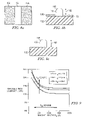
- FIGS. 3 a - 3 d illustrate partially depleted SOI transistors and a fully depleted SOI transistors of the present invention
- FIGS. 4 a and 4 b each provide a map showing the region of PD-SOI, FD-SOI, and multiple-gate transistors as a function of width Wand length L g for NMOS ( FIG. 4 a ) and PMOS ( FIG. 4 b ) transistors;
- FIG. 5 shows the three-dimensional perspective of a strained-channel multiple-gate transistor of one embodiment of the present invention
- FIGS. 6 a and 6 b provide charts that show that the strain-induced drive current enhancement is increased as the channel width is reduced;
- FIG. 7 shows the three-dimensional perspective of a strained-channel multiple-gate transistor where the silicon fin has rounded corners
- FIG. 8 a shows a top view of an active region or silicon fin
- FIGS. 8 b and 8 c provide cross-sectional views of the active region or silicon fin showing the rounded corner with shallow trench ( FIG. 8 b ) isolation or with mesa isolation ( FIG. 8 c );
- FIG. 9 provides a chart that shows that the stress in channel increases with reduced silicon film thickness and reduced gate length
- FIG. 10 provides a chart that shows that the stress in channel increases with reduced spacer width and reduced gate length
- FIG. 11 shows a cross-section of the semiconductor-on-insulator starting material
- FIGS. 12 a - 12 j provide cross-sections illustrating a process flow of one embodiment of the present invention.
- the present invention is related to co-pending applications Ser. No. 10/305,841 entitled “Strained-Channel Multiple-Gate Transistor”, filed Nov. 26, 2002 and Ser. No. 10/319,119 entitled “Semiconductor-on-Insulator Chip Incorporating Partially-Depleted, Fully-Depleted, and Multiple-Gate Devices”, filed Dec. 12, 2002. Aspects of the present invention provide improvements.
- the preferred embodiment of the present invention teaches a method and architecture to incorporate partially-depleted SOI (PD-SOI) and fully-depleted SOI (FD-SOI) transistors in the same chip, and, to provide enhanced strain effects to improve carrier mobilities and device performance in ultra-scaled devices.
- PD-SOI partially-depleted SOI
- FD-SOI fully-depleted SOI
- the preferred embodiment of the present invention employs a PD-SOI technology while implementing FD-SOI transistors by rearranging the transistor geometry, or by configuring the channel doping concentrations to achieve full transistor body depletion at selected channel lengths or channel widths. In this manner, it is possible to provide FD-SOI and PD-SOI transistors with similar silicon body thicknesses.
- planar FD-SOI type transistor where the depletion width is larger than the silicon thickness
- non-planar multiple-gate transistor or FinFET-like FD-SOI transistor which makes use of a novel device geometry to eliminate floating body effects.
- planar FD-SOI transistors have widths of more than 50 nm while non-planar fully-depleted multiple-gate transistors have widths of less than 50 nm.
- FIGS. 3 a - 3 d illustrate partially depleted SOI transistors and fully depleted SOI transistors of the present invention.
- the fully-depleted transistor of FIGS. 3 b uses a low body doping so that the maximum depletion width is larger than the silicon thickness to achieve full-depletion.
- the fully-depleted transistor of FIG. 3 d uses a novel geometry to allow the encroachment of gate electric field from the sides of the silicon body to achieve full body depletion.
- Super-halo doping and light body doping are designed to achieve FD-SOI and PD-SOI devices at different gate lengths, as shown in FIGS. 3 a and 3 b .
- a partially-depleted transistor device 100 is formed over a buried insulator 110 , while not shown, the buried insulator 110 is formed over a substrate, e.g., an undoped or lightly doped silicon substrate.
- the buried insulator 110 is typically an oxide such as silicon dioxide. Other insulators, such as silicon nitride or aluminum oxide, may alternatively be used. In some embodiments, the buried insulator can comprise a stack of layers, e.g., an oxide, nitride, oxide stack.
- Transistor device 100 is formed in a semiconductor layer 112 and includes a source region 114 and a drain region 116 .
- a gate 118 overlies a channel 120 and is separated therefrom by gate dielectric 122 .
- long-channel transistor 130 includes a source 132 , a drain 134 , a gate 136 , and a gate dielectric 138 .
- the transistor 130 can be formed in the same semiconductor layer 112 as transistor 100 or in a different semiconductor layer e.g., a different island or mesa on the same chips.
- the doping concentration in the super-halo region 140 is in the range of about 1 ⁇ 10 18 to about 2 ⁇ 10 19 dopants per cubic centimeter.
- the doping concentration in the lightly doped body region 142 is in the range of about 1 ⁇ 10 16 to about 1 ⁇ 10 18 dopants per cubic centimeter.
- the high super-halo doping concentration 140 in a short-channel transistor 100 results in a maximum depletion width that is smaller than the silicon film 112 thickness, and the transistor body is therefore partially-depleted.
- the gate 118 length increases, an increasing portion of the body region is constituted by the lightly doped body region 142 , and the effective body concentration decreases or the maximum depletion width increases.
- the long-channel transistor 130 has a light body-doping and a maximum depletion width that is larger than the silicon film 112 thickness, and the transistor body is fully-depleted.
- an active semiconductor layer region 155 includes a body region 154 and a depletion region 156 .
- the active region 155 is isolated from the other active regions by isolation region 158 .
- This isolation region 158 is preferably a shallow trench isolation (STI) region. It is understood that other isolation structures may be used.
- a gate electrode 160 is formed to surround the transistor active region, e.g., the channel region. Accordingly, an intentional recess 162 is formed within the isolation region 158 so that the semiconductor layer 155 includes sidewalls.
- the gate electrode 160 is adjacent to the top surface as well as the sidewalls of active layer 155 .
- a gate dielectric layer 164 is formed between the gate electrode 160 and the active layer 155 .
- the source and drain regions of the transistor device 150 are not shown in the illustration of FIG. 3 c .
- the channel current flows into and out of the page.
- one of the source/drain regions will be located in a plane above the page and the other located in a plane below the page.
- FIG. 3 d shows a similar structure for a FinFET-like transistor device 170 .
- Like elements from FIG. 3 c have been labeled with the same reference numerals.
- the active semiconductor layer is thin causing the body to be fully depleted.
- the planar partially-depleted transistor 150 of FIG. 3 c has a width that is much bigger than the maximum depletion layer width W d,max .
- the gate field encroaches from the isolation edges and eliminates the undepleted body region, thereby making the device of FIG. 3 d fully depleted.
- the resulting FD-SOI device has a non-planar geometry and is a multiple-gate transistor where the gate electrode 160 surrounds the transistor body 156 on multiple sides: the two sidewalls and the top surface.
- the multiple-gate transistor allows the encroachment of the gate electric field to the transistor body in the lateral direction, thus enhancing its ability to control short-channel effects.
- FIGS. 4 a and 4 b show the distribution of the PD-SOI and FD-SOI transistors according to the active region width W and the transistor gate length L g .
- FIG. 4 a provides data for NMOS devices and
- FIG. 4 b shows data for PMOS devices.
- Planar PD-SOI and FD-SOI transistors typically have active region width of more than 50 nm, while non-planar multiple-gate fully-depleted transistors generally have active region width of less than 50 nm.
- the results in FIG. 4 are obtained from an experiment where transistors are fabricated using a 65 nm PD-SOI-based process with a nominal gate length of 45 nm, a silicon body thickness of 40 nm, dual-doped poly-silicon gate electrodes, 14 angstroms nitrided gate oxide, and cobalt-silicided source/drain and gate.
- the PD-SOI region is smaller for P-channel transistors ( FIG. 4 b ) than for N-channel transistors ( FIG. 4 a ) because the impact ionization induced parasitic bipolar action is weaker in P-channel transistors.
- the transition from PD- to FD-SOI occurs as the gate length is increased.
- the non-planar FinFET-like or multiple-gate transistors are obtained at small width W, typically less than 50 nm.
- Wide-channel devices with smaller gate length L g are partially-depleted, showing a characteristic kink in the drain current I DS versus drain voltage V DS curves. As Wis reduced, transition from PD-SOI to FD-SOI occurs and the characteristic I DS -V DS kink disappears.
- PD-SOI and FD-SOI can be combined by using transistors with different combinations of W and L g .
- critical portions of the circuits may employ FD-SOI devices to achieve minimal floating body effects while the remaining portions of the circuits may employ PD-SOI devices.
- the critical portions of the circuits may include analog circuits and dynamic circuits.
- FIG. 5 illustrates a three-dimensional view of a multiple-gate FD-SOI transistor.
- the multiple-gate FD-SOI transistor has a gate electrode 160 on top of a gate dielectric layer 164 covering the two sidewalls as well as the top of a fin-like active region 155 .
- the gate dielectric 164 straddles across the fin 155 , wrapping around the fin 155 on the top surface 178 and the two sidewalls 176 of the fin or fin-like active region 155 .
- the gate electrode 160 is formed on the gate dielectric 164 , also wrapping around the fin-like active region 155 . Effectively, the gate electrode 160 forms three gates in the multiple-gate device: a gate on the top surface 178 of the fin 155 , and one gate on each of the two sidewalls 176 of the fin 155 .
- Shallow trench isolation filling materials 158 such as silicon oxide, as shown in FIG. 5 , may be used to fill the trenches surrounding the silicon fin 155 .
- other isolation techniques such as mesa isolation, as an example, may be used.
- mesa isolation When mesa isolation is used, no filling materials are used to fill the space surrounding the fin 155 . It is noted that the source 172 and drain 174 , which were not visible in the views shown in FIGS. 3 c and 3 d , can now be seen.
- FIG. 5 also shows the gate spacer 180 that surrounds the gate 160 .
- the gate space has a spacer width 182 .
- the gate also has a gate length 184 , which determines the channel length of the transistor.
- the channel width is determined by the size of the exposed fin sidewalls 176 and top surface 178 .
- novel transistor geometry according to this embodiment of the invention not only provides for the encroachment of electric field lines from the sides of the transistor to obtain full-body depletion and/or enhanced short-channel immunity, but also provides for enhanced strain effects.
- the enhancement of strain-induced transistor performance improvement provides one feature that can be incorporated with the present invention.
- the novel device geometry of this embodiments of the invention provides for enhanced strain effects as follows.
- the contact area between the silicon body and a stressor is increased by allowing the stressor to contact the silicon body on the sidewalls of the silicon body.
- strain in a strained channel transistor is enhanced.
- This technique is illustrated more clearly in a three-dimensional perspective of the multiple-gate transistor in FIG. 5 .
- the stressor 166 not only contacts the top surface of the silicon fin 155 , but also the sidewall surfaces of the silicon fin 155 .
- the additional contact area between the stressor 166 and the silicon fin 155 on the two sidewalls of the silicon fin results in enhanced stress effects in the silicon fin 155 .
- a strained-channel multiple-gate transistor may be formed with significantly enhanced performance.
- the arrows in FIG. 5 indicate the stress experienced by the channel region of the multiple-gate transistor.
- the stressor 166 may be a high-stress material such as silicon nitride (e.g., Si3N4) deposited by plasma-enhanced chemical vapor deposition (PECVD).
- PECVD plasma-enhanced chemical vapor deposition
- the stress in the PECVD silicon nitride can be in the range of ⁇ 500 mega-pascals (MPa) to 1500 MPa, where negative stress indicates compressive stress and positive stress indicates tensile stress.
- MPa mega-pascals
- the sidewall contact area as a proportion of the total contact area between the silicon fin 155 and the stressor 166 increases. Therefore, the enhancement in stress effects is expected to increase with a reduction in W.
- the silicon fin 155 of the multiple-gate transistor may have rounded corners 186 , as shown in the three-dimensional perspective of FIG. 7 .
- the stressor 166 is not shown for the sake of simplicity.
- the novel corner rounding at the isolation edge of the active region 155 of the multiple-gate transistor is another feature of the present invention to avoid double-hump I GS -V GS characteristics. Rounded corners, as compared with sharp corners, avoid excessive stress concentration in a small region that may result in defect generation and propagation. Such defects may result in degraded device performance and reduced yield.
- FIG. 8 a shows the top view of the active region 155 or silicon fin 155 after the patterning of an active region surrounded by isolation regions 158 .
- the cross-sectional view of this device is illustrated in FIG. 8 b , in which the isolation region 158 is depicted as a shallow trench isolation with an intentional recess 162 of amount R, where R may be greater than about 300 angstroms.
- a mesa isolation structure is used for isolation purposes.
- Mesa isolation is an isolation technique where silicon islands 155 are formed on an insulator 152 and electrically isolated from each other.
- the cross-sections in FIG. 8 b and FIG. 8 c emphasize the rounded corners 186 in the edge portions of the active region adjacent to the isolation regions.
- the radius of curvature of the round corner 186 is denoted by r.
- the value of r may vary from about 10 angstroms to about 200 angstroms in preferred embodiments.
- Corner rounding of the active silicon region 155 may be achieved by processes such as etching, oxidation, and/or annealing, performed after the active region definition. It is understood that the round corner in the sectional view are in fact two round top edges of the active region in a three dimensional view.
- FIGS. 8 b and 8 c schematically illustrate an intentional isolation recess 162 according to one example of the present invention.
- the recess R in both a shallow trench isolation or a mesa isolation is designed to be sufficiently large to allow the gate to deplete the narrow body from the isolation edges.
- the intentional recess will also give extra extended channel width.
- the value of R is preferably greater than about 300 angstroms. In general, R may be comparable to the thickness of the silicon film 155 .
- the transistor performance enhancement due to the strain effects increases with reduced transistor dimensions such as gate length 184 , spacer width 182 , and silicon film 155 thickness.
- reduction of the gate length 184 results in a larger strain-induced drive-current enhancement (dashed arrow). This is attributed to larger strain in the channel.
- the stress in the channel region of the silicon-on-insulator transistor is plotted as a function of the silicon film thickness for different gate lengths.
- the stress in the channel region increases as the silicon film 155 thickness is reduced and as the gate length 184 is reduced.
- the silicon film 155 thickness ranges from about 20 angstroms to about 400 angstroms.
- FIG. 10 shows that the stress in the channel increases as the spacer width 182 is reduced and as the gate length 184 is reduced.
- a spacer width of less than about 500 angstroms can be especially beneficial for significantly enhanced stress effects.
- the spacer width ranges from about 10 angstroms to about 500 angstroms.
- the starting material is a semiconductor-on-insulator wafer 200 as shown in FIG. 11 .
- the semiconductor-on-insulator wafer 200 includes a semiconductor layer 202 overlying an insulator layer 152 which in turn overlies a substrate 204 .
- the semiconductor layer 202 may be formed from an elemental semiconductor such as silicon or germanium, an alloy semiconductor such as silicon-germanium, or a compound semiconductor such as gallium arsenide or indium phosphide.
- the insulator layer 152 may be any insulating material such as silicon oxide, aluminum oxide, or silicon nitride or stacked combinations of these materials.
- the underlying substrate may be any semiconductor substrate such as silicon substrate or gallium arsenide substrate or non-semiconductor substrate such as quartz or sapphire. Other examples for each of these materials are envisioned.
- FIGS. 12 a - 12 j The method embodiment is more clearly illustrated in FIGS. 12 a - 12 j using a series of cross-sections depicting the transistor fabrication process.
- the cross-section of the device is taken in the plane containing the line A-A′ and parallel to the active region or silicon fin 155 as shown in FIG. 5 .
- the cross-section therefore cuts through the active region or silicon fin 155 , i.e., the source region 172 , channel region (unlabeled), drain region 174 , gate dielectric 164 , and the gate electrode 180 of the completed transistor.
- the portion of the gate 160 that overlies the sidewalls 176 of active region 155 is not shown because it is in a plane above (and below) the plane of the page.
- a silicon-on-insulator wafer 200 is used as the starting material, as shown in FIG. 12 a , where the semiconductor layer 202 is a silicon layer, the insulator layer 152 is a silicon oxide layer, and the substrate 204 is a silicon substrate. More preferably, the silicon layer 202 in the preferred embodiment has a thickness in the range of about 10 angstroms to about 2000 angstroms and the silicon oxide layer may have a thickness in the range of about 100 to about 2000 angstroms.
- An active region or silicon fin 155 is formed by patterning the silicon layer 202 , as shown in FIG. 12 b .
- the patterning of the active region or silicon fin 155 may be accomplished, for example, by depositing a mask material (not shown) on the silicon layer 202 , patterning the mask material by optical lithography to form a patterned mask, etching the silicon layer 202 , and removing the patterned mask.
- the mask material can be a photoresist, silicon nitride, or a stack comprising of a silicon nitride layer overlying a silicon oxide layer.
- a gate dielectric layer 164 is formed, as shown in FIG. 12 c .
- the gate dielectric layer 164 can have a thickness between about 3 to about 100 angstroms, as an example.
- the gate dielectric layer 164 on top 178 of the active region 155 can have a different thickness than the gate dielectric layer 164 on the two sidewalls 176 .
- the thickness of the gate dielectric layer 164 on the top 178 can be thinner than that on the sidewall 176 .
- the thickness of the gate dielectric layer 164 on top 178 of the active region 155 is less than about 20 angstroms.
- the gate dielectric 164 may comprise of any gate dielectric material such as silicon oxide, silicon oxynitride, or nitrided silicon oxide.
- the insulating material 164 may also be a high permittivity material with permittivity larger than 5, such as aluminum oxide (Al 2 O 3 ), hafnium oxide (HfO 2 ), halfnium silicon oxynitride (HfSiON), hafnium silicate (HfSiO 4 ), zirconium oxide (ZrO 2 ), zirconium silicate (ZrSiO 4 ) or lanthanum oxide (La 2 O 3 ).
- the gate dielectric is silicon oxide, which may be formed by thermal oxidation in an oxygen ambient at temperatures ranging from about 500 to about 1000 degrees Celsius.
- the gate dielectric layer 164 can also be formed by chemical vapor deposition or reactive sputtering. The gate dielectric layer 164 covers the top 178 and the sidewalls 176 of the silicon fin 155 .
- the gate electrode 160 material can then be formed on top of the gate dielectric layer 164 .
- the gate electrode 160 material can be comprised of conventional poly-crystalline silicon, poly-crystalline silicon germanium, metals, metallic silicides, metallic nitrides or other conductors.
- the gate electrode 160 material may be deposited by conventional techniques such as chemical vapor deposition.
- the gate electrode 160 may also be formed by the deposition of silicon and metal, followed by an anneal to form a metal silicide gate electrode material.
- the silicide could be titanium silicide, nickel silicide or cobalt silicide.
- FIG. 12 d shows the device cross-section after gate electrode 160 formation.
- the gate dielectric 164 is retained at least in the portion of the device covered by the gate electrode 160 .
- Source and drain extensions 186 and 188 are then implanted using ion implantation techniques as shown in FIG. 12 e .
- Super-halo implant may also be performed at this stage. By implanting the super-halo implant at a large angle ranging from about 15 to about 45 degrees with respect to the normal of the wafer, devices with short channel lengths will receive a high effective channel doping concentration, while devices with long channel lengths will receive a low effective channel doping concentration.
- the super halo implant creates super halo regions 190 .
- a spacer 180 is formed using techniques known and used in the art, e.g., deposition of the spacer material and anisotropic plasma etching as shown in FIG. 12 f .
- the spacer material may comprise of a dielectric material such as silicon nitride or silicon dioxide. In the preferred embodiment, the spacer 180 is made from silicon nitride.
- the source and drain regions 172 and 174 are implanted as shown in FIG. 12 g .
- the source and drain regions 172 and 174 can be strapped with one or more conductive materials such as metals and silicides 192 as shown in FIG. 12 h .
- the conductive materials 152 can reach the source and drain regions 172 and 174 through contacts on the sidewalls and/or the top of the active region 155 .
- a high-stress film or a stressor 166 is deposited over the completed transistor structure as shown in FIG. 12 i .
- the high stress film 166 not only contacts the top surface 178 of the active region 155 but also the sidewall surfaces 176 of the active region 155 , as shown in FIG. 5 .
- the high-stress film 166 can be PECVD silicon nitride. PECVD silicon nitride can be used to introduce tensile or compressive stress in the channel region.
- the residual film stress impacts the strain components in the channel.
- the residual film stress can be tailored from a high state of tension, for stoichiometric silicon nitride, to one of compression, for silicon-rich films.
- the tensile or compressive nature of the strain in the channel region can therefore be adjusted by varying process conditions such as temperature, pressure, and the ratio of the flow rate of a precursor gas, e.g., dichlorosilane, to the total gas flow rate.
- a passivation layer 194 is deposited with a thickness of a few thousand angstroms, e.g., about 1000 to about 5000 angstroms.
- the passivation layer 194 is preferably comprised of silicon oxide (e.g., formed by decomposition of TEOS or doped silicon oxide e.g., PSG or BPSG).
- Contact holes are etched through the passivation layer 194 and the high-stress film 166 and are filled with conductive materials 196 to electrically contact the source region 172 , drain region 174 , and gate electrode 160 of the transistor, as shown in FIG. 12 j .
- Metalization 198 can then be used to electrically couple these regions with other regions in the chip.
- one aspect of the present invention provides an improvement over PD-SOI or FD-SOI technologies.
- the present invention can selectively combine the advantages of PD-SOI and FD-SOI.
- this invention can achieve minimal floating body effects at critical circuits like analog circuits using FD-SOI devices, and can also have the freedom to adopt multiple threshold voltage V th devices in the PD-SOI region.
- Another noticeable improvement of the preferred embodiment of the present invention is its introduction of FinFET-like devices, which benefit scalability and control of short-channel effects.
- the semiconductor technology disclosed herein may be referred to as FinFET/FD/PD-SOI(“FiP-SOI”).
- FinFET/FD/PD-SOI “FiP-SOI”.
- yet another aspect of the invention is the provision of enhanced strain effects for improving transistor performance in the abovementioned transistors.
- the silicon fin 155 can be stressed by stressor layer 166 .
- the active area 155 can also be strained by way of the underlying layer.
- the silicon active area film can comprise a silicon layer formed over a silicon-geranium (SiGe) layer. The SiGe layer will cause a strain in the silicon layer.
- the silicon film for active area 155 can be formed using techniques taught in co-pending application Ser. No. 10/379,873 (TSMC2002-1384), filed Mar. 5, 2003, and incorporated herein by reference.
- the silicon layer 202 is formed on a donor substrate and attached above buried insulator 152 using wafer separation and bonding techniques. The various embodiments taught in the co-pending application can be utilized here.
Landscapes
- Thin Film Transistor (AREA)
- Insulated Gate Type Field-Effect Transistor (AREA)
Abstract
In accordance with a preferred embodiment of the present invention, a silicon-on-insulator (SOI) chip includes a silicon layer of a predetermined thickness overlying an insulator layer. A multiple-gate fully-depleted SOI MOSFET including a strained channel region is formed on a first portion of the silicon layer. A planar SOI MOSFET including a strained channel region formed on another portion of the silicon layer. For example, the planar SOI MOSFET can be a planar fully-depleted SOI (FD-SOI) MOSFET or the planar SOI MOSFET can be a planar partially-depleted SOI (PD-SOI) MOSFET.
Description
This invention is a divisional of Ser. No. 10/426,566, filed April 30, 2003, now U.S. Pat. No. 6,867,433.
The following U.S. patents and/or commonly assigned patent applications are hereby incorporated herein by reference:
| Patent or | Attorney | ||
| Ser. No. | Filing Date | Issue Date | Docket No. |
| 10/305,841 | Nov. 26, 2002 | TSMC2002-0895 | |
| 10/319,119 | Dec. 12, 2002 | TSMC2002-0979 | |
| 10/379,873 | Mar. 5, 2003 | TSMC2002-1384 | |
| 10/384,859 | Mar. 10, 2003 | TSMC2002-1385 | |
The present invention relates generally to the fabrication of semiconductor devices. More particularly, the preferred embodiment of the present invention relates to semiconductor-on-insulator chips incorporating partially-depleted, fully-depleted, and multiple-gate devices, and the introduction of strain in the channel of these devices.
Semiconductor device geometries have dramatically decreased in size since such devices were first introduced several decades ago. Since then, integrated circuits have generally followed the two year/half-size rule (often called Moore's Law), which means that the number of devices on a chip doubles every two years. Today's semiconductor fabrication plants are routinely producing devices having 130 nm and even 90 nm feature sizes.
The desire for higher performance circuits has driven the development of high-speed sub-100 nanometer (nm) silicon-on-insulator (SOI) complementary metal-oxide-semiconductor (CMOS) technology. In SOI technology, metal-oxide semiconductor field-effect transistors (MOSFETs) are formed on a thin layer of silicon overlying a layer of insulating material such as silicon oxide. Devices formed on SOI offer many advantages over their bulk counterparts, including reduced junction capacitance, absence of reverse body effect, soft-error immunity, full dielectric isolation, and absence of latch-up. SOI technology therefore enables higher speed performance, higher packing density, and reduced power consumption.
There are two types of conventional SOI devices: partially-depleted SOI (PD-SOI) devices, and fully-depleted (FD-SOI) devices. Conventional PD-SOI MOSFET is one in which the body thickness is thicker than the maximum depletion layer width Wd,max, and a conventional FD-SOI MOSFET is one in which the body thickness is thinner than Wd,max. The conventional PD-SOI and FD-SOI devices are planar devices, i.e., they are formed in the plane of the wafer.
It is noticed that remarkable progress has recently been achieved in PD-SOI technology. Although PD-SOI devices have the merit of being highly manufacturable, significant design burdens are faced by its users because of floating body effects. In PD-SOI devices, charge carriers generated by impact ionization near one source/drain region accumulate near the other source/drain region of the transistor. When sufficient carriers accumulate in the floating body, which is formed right below the channel region, the body potential is effectively altered.
Floating body effects occur in PD-SOI devices because of charge build-up in the floating body region. This results in kinks in the device current-voltage (I-V) curves, thereby degrading the electrical performance of the circuit. In general, the body potential of a PD-SOI device may vary during static, dynamic, or transient device operation, and is a function of many factors like temperature, voltage, circuit topology, and switching history. Therefore, circuit design using PD-SOI devices is not straightforward, and there is a significant barrier for the adoption of PD-SOI technology or the migration from bulk-Si design to PD-SOI design.
One traditional way to suppress floating body effects in PD-SOI devices is to provide an extra electrical connection to the body by adding a contact to the body for collection of current due to impact ionization. Various methods of making a contact to the body of a SOI transistor are known, but various disadvantages are known to be associated with these methods. One method for the suppression of the SOI floating-body effects is to use a linked-body device structure. However, the method is limited by a high body contact resistance.
Blake et al., in U.S. Pat. No. 4,946,799, described a process for making a body node to source node connection, where a contact region of the same conductivity type as the body node is formed within the source region in a self-aligned fashion, thus eliminating the floating body effects. In U.S. Pat. No. 6,387,739 issued to G. E. Smith III et al., a method for forming a body contact structure for SOI transistor is described.
Another way of avoiding floating body effects in SOI devices is to adopt a fully-depleted SOI (FD-SOI) technology. FD-SOI devices do not suffer from floating-body effects due to the fact that the body is fully-depleted. FD-SOI technology is therefore design-friendly since floating-body effects need not be accounted for in circuit design.
In a FD-SOI technology, devices with a low body-doping and/or a thin body thickness are used. Additionally, for good control of short-channel effects in ultra-scaled devices, the device body thickness is usually reduced to less than one third of gate length. Such a thin body thickness would require raised source/drain technology for series resistance reduction. However, raised source/drain formation, currently performed by selective epitaxy, is immature, expensive, pattern-density dependent, and may result in reduced manufacturing yield. In addition, SOI substrates with uniform ultra-thin Si films, as required for the manufacture of FD-SOI devices with ultra-thin body, are currently unavailable. Non-uniformity of the Si film thickness will result in significant fluctuations in the device characteristics and negatively impact the ease of manufacture.
U.S. Pat. No. 6,222,234, issued to K. Imai, describes a method for the fabrication of FD-SOI and PD-SOI devices on the same substrate. U.S. Pat. No. 6,414,355 issued to An et al. described the structure of silicon-on-insulator chips with an active layer of non-uniform thickness. U.S. Pat. No. 6,448,114 issued to An et al. described several methods of forming silicon-on-insulator chips with an active layer of non-uniform thickness. In these three patents, a SOI substrate with two different silicon film thicknesses is provided, where the FD-SOI devices reside in a region with a thinner silicon film, and the PD-SOI devices reside in a region with a thicker silicon film.
Other techniques have also been used to enhance transistor performance. For example, strain may be introduced in the transistor channel for improving carrier mobilities. Therefore, strain-induced mobility enhancement is another way to improve transistor performance in addition to device scaling.
In one approach, strain in the channel is introduced after the transistor is formed. In this approach, a high stress film 32 is formed over a completed transistor structure 30, as shown in FIG. 1 . The stressor 32, i.e., the high stress film, exerts significant influence on the channel 34, modifying the silicon lattice spacing in the channel region 34, and thus introducing strain in the channel region 34. As shown in FIG. 1 , the stressor is placed above the complete planar transistor structure, which includes a source 34 and a drain 38 formed in silicon region 40. A gate 42 overlies channel region 34 and is separated therefrom by gate dielectric 44. Sidewall spacer 46 can be included adjacent gate 42. This scheme is described in detail in a paper by A. Shimizu et at, entitled “Local mechanical stress control (LMC): a new technique for CMOS performance enhancement,” published in pp. 433-436 of the Digest of Technical Papers of the 2001 International Electron Device Meeting. The strain contributed by the high stress film is believed to be uniaxial in nature with a direction parallel to the source-to-drain direction.
In one embodiment, the present invention provides a method and system that overcomes the shortcomings of the prior art, and provides a highly manufacturable PD-SOI-like technology that produces FD-SOI type devices to eliminate floating body effects. Other embodiments of the invention provide a novel transistor geometry to magnify the effect of high-stress film on the channel strain. The present disclosure teaches a method of forming such a transistor.
In accordance with a preferred embodiment of the present invention, a silicon-on-insulator (SOI) chip includes a silicon layer of a predetermined thickness overlying an insulator layer. A multiple-gate fully-depleted SOI MOSFET including a strained channel region is formed on a first portion of the silicon layer. A planar SOI MOSFET including a strained channel region formed on another portion of the silicon layer. For example, the planar SOI MOSFET can be a planar fully-depleted SOI (FD-SOI) MOSFET or the planar SOI MOSFET can be a planar partially-depleted SOI (PD-SOI) MOSFET.
In accordance with another preferred embodiment of the present invention, an SOI chip including a multiple-gate fully-depleted SOI MOSFET has an insulator layer and a silicon fin overlying a portion of the insulator layer. A strained channel region formed in a portion of the silicon fin and a gate dielectric layer overlying the strained channel region is also included. A gate electrode is formed on the gate dielectric layer and a source region and a drain region is formed on portions of the semiconductor fin adjacent to the strained channel region, such that the source region is separated from the drain region by the strained channel region.
Another embodiment provides a method of forming a silicon-on-insulator device with a strained channel. In this method a silicon-on-insulator substrate that includes a silicon layer overlying an insulator layer is provided. At least one active region is defined in the silicon layer. A gate dielectric layer is formed in the active region and a gate electrode is formed on the gate dielectric layer. Source and drain regions can then be formed adjacent to the gate electrode and a high-stress film covers the gate electrode, source region, and drain region.
The foregoing has outlined rather broadly the features and technical advantages of the present invention in order that the detailed description of the invention that follows may be better understood. Additional features and advantages of the invention will be described hereinafter which form the subject of the claims of the invention. It should be appreciated by those skilled in the art that the conception and specific embodiment disclosed may be readily utilized as a basis for modifying or designing other structures or processes for carrying out the same purposes of the present invention. It should also be realized by those skilled in the art that such equivalent constructions do not depart from the spirit and scope of the invention as set forth in the appended claims.
For a more complete understanding of the present invention, and the advantages thereof, reference is now made to the following descriptions taken in conjunction with the accompanying drawing, in which:
The present invention is related to co-pending applications Ser. No. 10/305,841 entitled “Strained-Channel Multiple-Gate Transistor”, filed Nov. 26, 2002 and Ser. No. 10/319,119 entitled “Semiconductor-on-Insulator Chip Incorporating Partially-Depleted, Fully-Depleted, and Multiple-Gate Devices”, filed Dec. 12, 2002. Aspects of the present invention provide improvements.
For example, the preferred embodiment of the present invention teaches a method and architecture to incorporate partially-depleted SOI (PD-SOI) and fully-depleted SOI (FD-SOI) transistors in the same chip, and, to provide enhanced strain effects to improve carrier mobilities and device performance in ultra-scaled devices. Unlike other devices that utilize different silicon thicknesses to the achieve FD-SOI and PD-SOI transistors on the same chip, the preferred embodiment of the present invention employs a PD-SOI technology while implementing FD-SOI transistors by rearranging the transistor geometry, or by configuring the channel doping concentrations to achieve full transistor body depletion at selected channel lengths or channel widths. In this manner, it is possible to provide FD-SOI and PD-SOI transistors with similar silicon body thicknesses.
Two types of FD-SOI transistors are provided on the same chip: a planar FD-SOI type transistor where the depletion width is larger than the silicon thickness; and a non-planar multiple-gate transistor or FinFET-like FD-SOI transistor, which makes use of a novel device geometry to eliminate floating body effects. In general, planar FD-SOI transistors have widths of more than 50 nm while non-planar fully-depleted multiple-gate transistors have widths of less than 50 nm.
Concepts of the preferred embodiment of-this invention are more clearly illustrated in FIGS. 3 a-3 d. FIGS. 3 a-3 d illustrate partially depleted SOI transistors and fully depleted SOI transistors of the present invention. The fully-depleted transistor of FIGS. 3 b uses a low body doping so that the maximum depletion width is larger than the silicon thickness to achieve full-depletion. The fully-depleted transistor of FIG. 3 d uses a novel geometry to allow the encroachment of gate electric field from the sides of the silicon body to achieve full body depletion.
Super-halo doping and light body doping are designed to achieve FD-SOI and PD-SOI devices at different gate lengths, as shown in FIGS. 3 a and 3 b. Referring first to FIG. 3 a, a partially-depleted transistor device 100 is formed over a buried insulator 110, while not shown, the buried insulator 110 is formed over a substrate, e.g., an undoped or lightly doped silicon substrate.
The buried insulator 110 is typically an oxide such as silicon dioxide. Other insulators, such as silicon nitride or aluminum oxide, may alternatively be used. In some embodiments, the buried insulator can comprise a stack of layers, e.g., an oxide, nitride, oxide stack.
Similarly long-channel transistor 130 includes a source 132, a drain 134, a gate 136, and a gate dielectric 138. The transistor 130 can be formed in the same semiconductor layer 112 as transistor 100 or in a different semiconductor layer e.g., a different island or mesa on the same chips.
One feature is the design of the super-halo doping 140 in FIG. 3 b (or double halo doping 140 in FIG. 3 a) and light body doping 142 such that the effective doping concentration of the transistor body decreases as the gate length is increased. The doping concentration in the super-halo region 140 is in the range of about 1×10¹⁸ to about 2×10¹⁹ dopants per cubic centimeter. The doping concentration in the lightly doped body region 142 is in the range of about 1×10¹⁶ to about 1×10¹⁸ dopants per cubic centimeter.
In FIG. 3 a, the high super-halo doping concentration 140 in a short-channel transistor 100 results in a maximum depletion width that is smaller than the silicon film 112 thickness, and the transistor body is therefore partially-depleted. As the gate 118 length increases, an increasing portion of the body region is constituted by the lightly doped body region 142, and the effective body concentration decreases or the maximum depletion width increases. In FIG. 3 b, the long-channel transistor 130 has a light body-doping and a maximum depletion width that is larger than the silicon film 112 thickness, and the transistor body is fully-depleted.
Referring now to FIGS. 3 c and 3 d, another way to achieve full depletion in the transistor body is to allow the electric field lines to encroach from the sides of the transistor body by using a novel transistor geometry. Referring now to FIG. 3 c, a transistor 150 is formed over a buried insulator. The buried insulator 152 can include any of the characteristics described above with respect to insulator 110 and may be formed on a substrate, where the discussion above with respect to FIGS. 3 a and 3 b equally applies here. In this device, an active semiconductor layer region 155 includes a body region 154 and a depletion region 156. The active region 155 is isolated from the other active regions by isolation region 158. This isolation region 158 is preferably a shallow trench isolation (STI) region. It is understood that other isolation structures may be used.
A gate electrode 160 is formed to surround the transistor active region, e.g., the channel region. Accordingly, an intentional recess 162 is formed within the isolation region 158 so that the semiconductor layer 155 includes sidewalls. The gate electrode 160 is adjacent to the top surface as well as the sidewalls of active layer 155. A gate dielectric layer 164 is formed between the gate electrode 160 and the active layer 155.
The source and drain regions of the transistor device 150 are not shown in the illustration of FIG. 3 c. In this case, the channel current flows into and out of the page. As a result, one of the source/drain regions will be located in a plane above the page and the other located in a plane below the page.
One feature of the novel transistor geometry is the intentional recess 162 in the isolation region 158, as shown in FIGS. 3 c and 3 d. The planar partially-depleted transistor 150 of FIG. 3 c has a width that is much bigger than the maximum depletion layer width Wd,max. When the active region width W (see FIG. 3 d) is reduced to less than twice the depletion width layer in the body, the gate field encroaches from the isolation edges and eliminates the undepleted body region, thereby making the device of FIG. 3 d fully depleted.
The resulting FD-SOI device has a non-planar geometry and is a multiple-gate transistor where the gate electrode 160 surrounds the transistor body 156 on multiple sides: the two sidewalls and the top surface. By having a gate electrode 160 that surrounds the transistor body 155, the multiple-gate transistor allows the encroachment of the gate electric field to the transistor body in the lateral direction, thus enhancing its ability to control short-channel effects.
The preferred embodiment of this invention teaches a unique way of incorporating PD-SOI and FD-SOI transistors on the same chip using the same process technology, with a distribution of FD-SOI and PD-SOI transistors according to transistor dimensions. FIGS. 4 a and 4 b show the distribution of the PD-SOI and FD-SOI transistors according to the active region width W and the transistor gate length Lg. FIG. 4 a provides data for NMOS devices and FIG. 4 b shows data for PMOS devices. These figures provide a map showing the region of PD-SOI transistors (gray region), conventional FD-SOI transistors (white region), and multiple-gate transistors (in region enclosed by dashed box) as a function of width Wand length Lg for NMOS and PMOS transistors.
Planar PD-SOI and FD-SOI transistors typically have active region width of more than 50 nm, while non-planar multiple-gate fully-depleted transistors generally have active region width of less than 50 nm. The results in FIG. 4 are obtained from an experiment where transistors are fabricated using a 65 nm PD-SOI-based process with a nominal gate length of 45 nm, a silicon body thickness of 40 nm, dual-doped poly-silicon gate electrodes, 14 angstroms nitrided gate oxide, and cobalt-silicided source/drain and gate.
The PD-SOI region is smaller for P-channel transistors (FIG. 4 b) than for N-channel transistors (FIG. 4 a) because the impact ionization induced parasitic bipolar action is weaker in P-channel transistors. The transition from PD- to FD-SOI occurs as the gate length is increased. In addition, the non-planar FinFET-like or multiple-gate transistors are obtained at small width W, typically less than 50 nm. Wide-channel devices with smaller gate length Lg are partially-depleted, showing a characteristic kink in the drain current IDS versus drain voltage VDS curves. As Wis reduced, transition from PD-SOI to FD-SOI occurs and the characteristic IDS-VDS kink disappears.
It is clear that the advantages of PD-SOI and FD-SOI can be combined by using transistors with different combinations of W and Lg. For example, when converting a circuit design for bulk technology to a circuit design for SOI technology, critical portions of the circuits may employ FD-SOI devices to achieve minimal floating body effects while the remaining portions of the circuits may employ PD-SOI devices. For example, the critical portions of the circuits may include analog circuits and dynamic circuits.
The quasi-planar device structure or geometry of the multiple-gate FD-SOI transistor will now be described further. FIG. 5 illustrates a three-dimensional view of a multiple-gate FD-SOI transistor. The multiple-gate FD-SOI transistor has a gate electrode 160 on top of a gate dielectric layer 164 covering the two sidewalls as well as the top of a fin-like active region 155. The gate dielectric 164 straddles across the fin 155, wrapping around the fin 155 on the top surface 178 and the two sidewalls 176 of the fin or fin-like active region 155. The gate electrode 160 is formed on the gate dielectric 164, also wrapping around the fin-like active region 155. Effectively, the gate electrode 160 forms three gates in the multiple-gate device: a gate on the top surface 178 of the fin 155, and one gate on each of the two sidewalls 176 of the fin 155.
Shallow trench isolation filling materials 158 such as silicon oxide, as shown in FIG. 5 , may be used to fill the trenches surrounding the silicon fin 155. However, other isolation techniques, such as mesa isolation, as an example, may be used. When mesa isolation is used, no filling materials are used to fill the space surrounding the fin 155. It is noted that the source 172 and drain 174, which were not visible in the views shown in FIGS. 3 c and 3 d, can now be seen.
The novel transistor geometry according to this embodiment of the invention not only provides for the encroachment of electric field lines from the sides of the transistor to obtain full-body depletion and/or enhanced short-channel immunity, but also provides for enhanced strain effects. The enhancement of strain-induced transistor performance improvement provides one feature that can be incorporated with the present invention.
The novel device geometry of this embodiments of the invention provides for enhanced strain effects as follows. The contact area between the silicon body and a stressor is increased by allowing the stressor to contact the silicon body on the sidewalls of the silicon body. As a result of the increased influence of the stressor on the active region, strain in a strained channel transistor is enhanced. This technique is illustrated more clearly in a three-dimensional perspective of the multiple-gate transistor in FIG. 5 . The stressor 166 not only contacts the top surface of the silicon fin 155, but also the sidewall surfaces of the silicon fin 155. The additional contact area between the stressor 166 and the silicon fin 155 on the two sidewalls of the silicon fin results in enhanced stress effects in the silicon fin 155. As a result, a strained-channel multiple-gate transistor may be formed with significantly enhanced performance. The arrows in FIG. 5 indicate the stress experienced by the channel region of the multiple-gate transistor.
The stressor 166 may be a high-stress material such as silicon nitride (e.g., Si3N4) deposited by plasma-enhanced chemical vapor deposition (PECVD). The stress in the PECVD silicon nitride can be in the range of −500 mega-pascals (MPa) to 1500 MPa, where negative stress indicates compressive stress and positive stress indicates tensile stress. As the channel width W decreases, the sidewall contact area as a proportion of the total contact area between the silicon fin 155 and the stressor 166 increases. Therefore, the enhancement in stress effects is expected to increase with a reduction in W.
This prediction of enhanced drive current is confirmed by our experimental results as shown in FIGS. 6 a and 6 b. Strain-induced drive current enhancement is increased from 10% to 17% as the Wis reduced from 1200 nm to 110 nm at an off-state leakage of 300 nA/micrometer. With further scaling of the gate length, the enhancement (dashed arrow) will become even larger, which is attributed to larger channel stress. Operation voltage is 1.0 V.
The silicon fin 155 of the multiple-gate transistor may have rounded corners 186, as shown in the three-dimensional perspective of FIG. 7 . In FIG. 7 , the stressor 166 is not shown for the sake of simplicity. The novel corner rounding at the isolation edge of the active region 155 of the multiple-gate transistor is another feature of the present invention to avoid double-hump IGS-VGS characteristics. Rounded corners, as compared with sharp corners, avoid excessive stress concentration in a small region that may result in defect generation and propagation. Such defects may result in degraded device performance and reduced yield.
In another embodiment, as shown in FIG. 8 c, a mesa isolation structure is used for isolation purposes. Mesa isolation is an isolation technique where silicon islands 155 are formed on an insulator 152 and electrically isolated from each other. The cross-sections in FIG. 8 b and FIG. 8 c emphasize the rounded corners 186 in the edge portions of the active region adjacent to the isolation regions.
The radius of curvature of the round corner 186 is denoted by r. The value of r may vary from about 10 angstroms to about 200 angstroms in preferred embodiments. Corner rounding of the active silicon region 155 may be achieved by processes such as etching, oxidation, and/or annealing, performed after the active region definition. It is understood that the round corner in the sectional view are in fact two round top edges of the active region in a three dimensional view.
In addition, according to simulation and experimental results, the transistor performance enhancement due to the strain effects increases with reduced transistor dimensions such as gate length 184, spacer width 182, and silicon film 155 thickness. As shown experimentally in FIG. 6 , reduction of the gate length 184 results in a larger strain-induced drive-current enhancement (dashed arrow). This is attributed to larger strain in the channel.
In FIG. 9 , the stress in the channel region of the silicon-on-insulator transistor is plotted as a function of the silicon film thickness for different gate lengths. The stress in the channel region increases as the silicon film 155 thickness is reduced and as the gate length 184 is reduced. In the preferred embodiment, the silicon film 155 thickness ranges from about 20 angstroms to about 400 angstroms. FIG. 10 shows that the stress in the channel increases as the spacer width 182 is reduced and as the gate length 184 is reduced. According to embodiments of this invention, a spacer width of less than about 500 angstroms can be especially beneficial for significantly enhanced stress effects. In the preferred embodiment, the spacer width ranges from about 10 angstroms to about 500 angstroms.
According to the next embodiment of this invention, a method of providing the abovementioned semiconductor-on-insulator chip with strained-channel partially-depleted SOI transistors, fully-depleted SOI transistors, and multiple-gate transistors will be described. The starting material is a semiconductor-on-insulator wafer 200 as shown in FIG. 11 . The semiconductor-on-insulator wafer 200, includes a semiconductor layer 202 overlying an insulator layer 152 which in turn overlies a substrate 204. It is understood that the semiconductor layer 202 may be formed from an elemental semiconductor such as silicon or germanium, an alloy semiconductor such as silicon-germanium, or a compound semiconductor such as gallium arsenide or indium phosphide. The insulator layer 152 may be any insulating material such as silicon oxide, aluminum oxide, or silicon nitride or stacked combinations of these materials. The underlying substrate may be any semiconductor substrate such as silicon substrate or gallium arsenide substrate or non-semiconductor substrate such as quartz or sapphire. Other examples for each of these materials are envisioned.
The method embodiment is more clearly illustrated in FIGS. 12 a-12 j using a series of cross-sections depicting the transistor fabrication process. The cross-section of the device is taken in the plane containing the line A-A′ and parallel to the active region or silicon fin 155 as shown in FIG. 5 . The cross-section therefore cuts through the active region or silicon fin 155, i.e., the source region 172, channel region (unlabeled), drain region 174, gate dielectric 164, and the gate electrode 180 of the completed transistor. In this view the portion of the gate 160 that overlies the sidewalls 176 of active region 155 is not shown because it is in a plane above (and below) the plane of the page.
In the preferred embodiment, a silicon-on-insulator wafer 200 is used as the starting material, as shown in FIG. 12 a, where the semiconductor layer 202 is a silicon layer, the insulator layer 152 is a silicon oxide layer, and the substrate 204 is a silicon substrate. More preferably, the silicon layer 202 in the preferred embodiment has a thickness in the range of about 10 angstroms to about 2000 angstroms and the silicon oxide layer may have a thickness in the range of about 100 to about 2000 angstroms.
An active region or silicon fin 155 is formed by patterning the silicon layer 202, as shown in FIG. 12 b. The patterning of the active region or silicon fin 155 may be accomplished, for example, by depositing a mask material (not shown) on the silicon layer 202, patterning the mask material by optical lithography to form a patterned mask, etching the silicon layer 202, and removing the patterned mask. The mask material can be a photoresist, silicon nitride, or a stack comprising of a silicon nitride layer overlying a silicon oxide layer.
A gate dielectric layer 164 is formed, as shown in FIG. 12 c. The gate dielectric layer 164 can have a thickness between about 3 to about 100 angstroms, as an example. The gate dielectric layer 164 on top 178 of the active region 155 can have a different thickness than the gate dielectric layer 164 on the two sidewalls 176. For example, the thickness of the gate dielectric layer 164 on the top 178 can be thinner than that on the sidewall 176. In some examples, the thickness of the gate dielectric layer 164 on top 178 of the active region 155 is less than about 20 angstroms.
The gate dielectric 164 may comprise of any gate dielectric material such as silicon oxide, silicon oxynitride, or nitrided silicon oxide. The insulating material 164 may also be a high permittivity material with permittivity larger than 5, such as aluminum oxide (Al2O3), hafnium oxide (HfO2), halfnium silicon oxynitride (HfSiON), hafnium silicate (HfSiO4), zirconium oxide (ZrO2), zirconium silicate (ZrSiO4) or lanthanum oxide (La2O3). In the preferred embodiment, the gate dielectric is silicon oxide, which may be formed by thermal oxidation in an oxygen ambient at temperatures ranging from about 500 to about 1000 degrees Celsius. The gate dielectric layer 164 can also be formed by chemical vapor deposition or reactive sputtering. The gate dielectric layer 164 covers the top 178 and the sidewalls 176 of the silicon fin 155.
With the gate dielectric layer 164 appropriately formed, the gate electrode 160 material can then be formed on top of the gate dielectric layer 164. The gate electrode 160 material can be comprised of conventional poly-crystalline silicon, poly-crystalline silicon germanium, metals, metallic silicides, metallic nitrides or other conductors. The gate electrode 160 material may be deposited by conventional techniques such as chemical vapor deposition. The gate electrode 160 may also be formed by the deposition of silicon and metal, followed by an anneal to form a metal silicide gate electrode material. An example, the silicide could be titanium silicide, nickel silicide or cobalt silicide.
The gate electrode 160 material is then patterned using photolithography techniques, and etched using plasma etch processes to form the gate electrodes. FIG. 12 d shows the device cross-section after gate electrode 160 formation. The gate dielectric 164 is retained at least in the portion of the device covered by the gate electrode 160.
Source and drain extensions 186 and 188 are then implanted using ion implantation techniques as shown in FIG. 12 e. Super-halo implant may also be performed at this stage. By implanting the super-halo implant at a large angle ranging from about 15 to about 45 degrees with respect to the normal of the wafer, devices with short channel lengths will receive a high effective channel doping concentration, while devices with long channel lengths will receive a low effective channel doping concentration.
The super halo implant creates super halo regions 190. A spacer 180 is formed using techniques known and used in the art, e.g., deposition of the spacer material and anisotropic plasma etching as shown in FIG. 12 f. The spacer material may comprise of a dielectric material such as silicon nitride or silicon dioxide. In the preferred embodiment, the spacer 180 is made from silicon nitride.
Following spacer formation, the source and drain regions 172 and 174 are implanted as shown in FIG. 12 g. The source and drain regions 172 and 174 can be strapped with one or more conductive materials such as metals and silicides 192 as shown in FIG. 12 h. The conductive materials 152 can reach the source and drain regions 172 and 174 through contacts on the sidewalls and/or the top of the active region 155.
Next, a high-stress film or a stressor 166 is deposited over the completed transistor structure as shown in FIG. 12 i. According to preferred embodiment of this invention, the high stress film 166 not only contacts the top surface 178 of the active region 155 but also the sidewall surfaces 176 of the active region 155, as shown in FIG. 5 . As an example, the high-stress film 166 can be PECVD silicon nitride. PECVD silicon nitride can be used to introduce tensile or compressive stress in the channel region.
The residual film stress impacts the strain components in the channel. The residual film stress can be tailored from a high state of tension, for stoichiometric silicon nitride, to one of compression, for silicon-rich films. The tensile or compressive nature of the strain in the channel region can therefore be adjusted by varying process conditions such as temperature, pressure, and the ratio of the flow rate of a precursor gas, e.g., dichlorosilane, to the total gas flow rate.
Following the formation of the high-stress film 166, a passivation layer 194 is deposited with a thickness of a few thousand angstroms, e.g., about 1000 to about 5000 angstroms. The passivation layer 194 is preferably comprised of silicon oxide (e.g., formed by decomposition of TEOS or doped silicon oxide e.g., PSG or BPSG). Contact holes are etched through the passivation layer 194 and the high-stress film 166 and are filled with conductive materials 196 to electrically contact the source region 172, drain region 174, and gate electrode 160 of the transistor, as shown in FIG. 12 j. Metalization 198 can then be used to electrically couple these regions with other regions in the chip.
In summary, one aspect of the present invention provides an improvement over PD-SOI or FD-SOI technologies. The present invention can selectively combine the advantages of PD-SOI and FD-SOI. For example, when converting circuit design from bulk to SOI, this invention can achieve minimal floating body effects at critical circuits like analog circuits using FD-SOI devices, and can also have the freedom to adopt multiple threshold voltage Vth devices in the PD-SOI region. Another noticeable improvement of the preferred embodiment of the present invention is its introduction of FinFET-like devices, which benefit scalability and control of short-channel effects. The semiconductor technology disclosed herein may be referred to as FinFET/FD/PD-SOI(“FiP-SOI”). In yet another aspect of the invention is the provision of enhanced strain effects for improving transistor performance in the abovementioned transistors.
As discussed above, the silicon fin 155 can be stressed by stressor layer 166. The active area 155 can also be strained by way of the underlying layer. For example; the silicon active area film can comprise a silicon layer formed over a silicon-geranium (SiGe) layer. The SiGe layer will cause a strain in the silicon layer.
In another embodiment, the silicon film for active area 155 can be formed using techniques taught in co-pending application Ser. No. 10/379,873 (TSMC2002-1384), filed Mar. 5, 2003, and incorporated herein by reference. In this embodiment, the silicon layer 202 is formed on a donor substrate and attached above buried insulator 152 using wafer separation and bonding techniques. The various embodiments taught in the co-pending application can be utilized here.
In the foregoing specification, the invention has been described with reference to specific embodiments. However, various modifications and changes can be made by one skilled in the art without departing from the scope of the present invention. Accordingly, the specification and figures are to be regarded in an illustrative rather than a restrictive sense, and all such modifications are intended to be included within the scope of the present invention. It is understood that several modifications, changes and substitutions are intended in the foregoing disclosure and in some instances some features of the invention will be employed without a corresponding use of other features. Accordingly, it is appropriate that the appended claims be construed broadly and in a manner consistent with the scope of the invention.
Claims (26)
1. A method of forming a silicon-on-insulator device with a strained channel, the method comprising:
providing a silicon-on-insulator substrate, the substrate comprising a plurality of silicon fins electrically isolated from each other by shallow trench isolation, each silicon fin of said plurality extending between first and second ends and overlying at least one portion of an insulator layer, and each of said silicon fins defining an active region having a top surface and a pair of sidewalls;
forming a gate dielectric layer, over an intermediate portion of said top surface and said pair of sidewalls of said plurality of said silicon fins;
forming a gate electrode covering the gate dielectric layer;
forming source and drain regions in each of said silicon fins, one each of said source and drain region adjacent to one of said first and second ends and each adjacent to the gate electrode;
forming a high-stress film covering the gate electrode, source region, and drain region.
2. The method of claim 1 wherein the high stress film contacts the sidewall surfaces of the active region.
3. The method of claim 1 and further comprising after forming the gate electrode, forming source and drain extension regions.
4. The method of claim 3 wherein the source and drain extension regions are formed by ion implantation.
5. The method of claim 3 and further comprising, after forming the source and drain extension regions, forming super halo region.
6. The method of claim 5 wherein the super halo region is formed by ion implantation.
7. The method of claim 5 wherein the super halo region has a doping concentration in the range of about 1×10¹⁸ to about 2×1019 cm−3.
8. The method of claim 3 , and further comprising, after of forming the source and drain extension regions, forming spacers adjacent to the gate electrode.
9. The method of claim 8 wherein the spacers are formed by chemical vapor deposition of spacer material followed by anisotropic plasma etching.
10. The method of claim 8 wherein the spacers have a width of less than about 500 angstroms.
11. The method of claim 1 wherein the silicon fin has a thickness in the range of about 10 angstroms to about 2000 angstroms.
12. The method of claim 1 wherein the silicon fin has a thickness of less than about 200 angstroms.
13. A method of forming a silicon-on-insulator device with a strained channel, the method comprising:
providing a silicon-on-insulator substrate, the substrate comprising a silicon layer overlying an insulator layer;
defining at least one active region in the silicon layer, said active region having rounded corners, said rounded corners having a radius of about 10 angstroms to about 200 angstroms;
forming a gate dielectric layer in the active region;
forming a gate electrode on the gate dielectric layer;
forming source and drain regions adjacent to the gate electrode; and
forming a high-stress film covering the gate electrode, source region, and drain region.
14. The method of claim 13 wherein the high stress film contacts said pair of sidewalls of the active region.
15. The method of claim 13 and further comprising after forming the gate electrode, forming source and drain extension regions.
16. The method of claim 15 wherein the source and drain extension regions are formed by ion implantation.
17. The method of claim 15 and further comprising, after forming the source and drain extension regions, forming super halo region.
18. The method of claim 17 wherein the super halo region is formed by ion implantation.
19. The method of claim 17 wherein the super halo region has a doping concentration in the range of about 1×10¹⁸ to about 2×1019 cm−3.
20. The method of claim 15 , and further comprising, after of forming the source and drain extension regions, forming spacers adjacent to the gate electrode.
21. The method of claim 20 wherein the spacers are formed by chemical vapor deposition of spacer material followed by anisotropic plasma etching.
22. The method of claim 20 wherein the spacers have a width of less than about 500 angstroms.
23. The method of claim 13 wherein the silicon layer has a thickness in the range of about 10 angstroms to about 2000 angstroms.
24. The method of claim 13 wherein the silicon layer has a thickness of less than about 200 angstroms.
25. The method of claim 13 wherein the at least one active region comprises a plurality of active regions that are electrically isolated from each other by shallow trench isolation.
26. The method of claim 13 wherein the at least one active region comprises a plurality of active regions that are electrically isolated from each other by mesa isolation.
Priority Applications (1)
| Application Number | Priority Date | Filing Date | Title |
|---|---|---|---|
| US10/999,564 US7268024B2 (en) | 2003-04-30 | 2004-11-29 | Semiconductor-on-insulator chip incorporating strained-channel partially-depleted, fully-depleted, and multiple-gate transistors |
Applications Claiming Priority (2)
| Application Number | Priority Date | Filing Date | Title |
|---|---|---|---|
| US10/426,566 US6867433B2 (en) | 2003-04-30 | 2003-04-30 | Semiconductor-on-insulator chip incorporating strained-channel partially-depleted, fully-depleted, and multiple-gate transistors |
| US10/999,564 US7268024B2 (en) | 2003-04-30 | 2004-11-29 | Semiconductor-on-insulator chip incorporating strained-channel partially-depleted, fully-depleted, and multiple-gate transistors |
Related Parent Applications (1)
| Application Number | Title | Priority Date | Filing Date |
|---|---|---|---|
| US10/426,566 Division US6867433B2 (en) | 2003-04-30 | 2003-04-30 | Semiconductor-on-insulator chip incorporating strained-channel partially-depleted, fully-depleted, and multiple-gate transistors |
Publications (2)
| Publication Number | Publication Date |
|---|---|
| US20050093067A1 US20050093067A1 (en) | 2005-05-05 |
| US7268024B2 true US7268024B2 (en) | 2007-09-11 |
Family
ID=33309898
Family Applications (2)
| Application Number | Title | Priority Date | Filing Date |
|---|---|---|---|
| US10/426,566 Expired - Lifetime US6867433B2 (en) | 2003-04-30 | 2003-04-30 | Semiconductor-on-insulator chip incorporating strained-channel partially-depleted, fully-depleted, and multiple-gate transistors |
| US10/999,564 Expired - Lifetime US7268024B2 (en) | 2003-04-30 | 2004-11-29 | Semiconductor-on-insulator chip incorporating strained-channel partially-depleted, fully-depleted, and multiple-gate transistors |
Family Applications Before (1)
| Application Number | Title | Priority Date | Filing Date |
|---|---|---|---|
| US10/426,566 Expired - Lifetime US6867433B2 (en) | 2003-04-30 | 2003-04-30 | Semiconductor-on-insulator chip incorporating strained-channel partially-depleted, fully-depleted, and multiple-gate transistors |
Country Status (4)
| Country | Link |
|---|---|
| US (2) | US6867433B2 (en) |
| CN (2) | CN1293635C (en) |
| SG (1) | SG143035A1 (en) |
| TW (1) | TWI255043B (en) |
Cited By (37)
| Publication number | Priority date | Publication date | Assignee | Title |
|---|---|---|---|---|
| US20070246793A1 (en) * | 2006-04-24 | 2007-10-25 | Freescale Semiconductor, Inc. | Electronic device including a semiconductor layer and another layer adjacent to an opening within the semiconductor layer and a process of forming the same |
| US20070264839A1 (en) * | 2006-05-12 | 2007-11-15 | Freescale Semiconductor, Inc. | Process of forming electronic device including a densified nitride layer adjacent to an opening within a semiconductor layer |
| US7491622B2 (en) | 2006-04-24 | 2009-02-17 | Freescale Semiconductor, Inc. | Process of forming an electronic device including a layer formed using an inductively coupled plasma |
| US7736956B2 (en) | 2005-08-17 | 2010-06-15 | Intel Corporation | Lateral undercut of metal gate in SOI device |
| US7790540B2 (en) | 2006-08-25 | 2010-09-07 | International Business Machines Corporation | Structure and method to use low k stress liner to reduce parasitic capacitance |
| US20100244139A1 (en) * | 2004-06-24 | 2010-09-30 | International Business Machines Corporation | Strained-silicon cmos device and method |
| US7808051B2 (en) | 2008-09-29 | 2010-10-05 | Taiwan Semiconductor Manufacturing Company, Ltd. | Standard cell without OD space effect in Y-direction |
| US20110020987A1 (en) * | 2003-06-27 | 2011-01-27 | Hareland Scott A | Nonplanar semiconductor device with partially or fully wrapped around gate electrode and methods of fabrication |
| US7915167B2 (en) | 2004-09-29 | 2011-03-29 | Intel Corporation | Fabrication of channel wraparound gate structure for field-effect transistor |
| US7943961B2 (en) | 2008-03-13 | 2011-05-17 | Taiwan Semiconductor Manufacturing Company, Ltd. | Strain bars in stressed layers of MOS devices |
| US7960801B2 (en) | 2005-11-03 | 2011-06-14 | International Business Machines Corporation | Gate electrode stress control for finFET performance enhancement description |
| US7960794B2 (en) | 2004-08-10 | 2011-06-14 | Intel Corporation | Non-planar pMOS structure with a strained channel region and an integrated strained CMOS flow |
| US20110171788A1 (en) * | 2010-01-11 | 2011-07-14 | International Business Machines Corporation | Fabrication of Field Effect Devices Using Spacers |
| US20110223736A1 (en) * | 2010-03-09 | 2011-09-15 | Taiwan Semiconductor Manufacturing Company, Ltd. | LDD Epitaxy for FinFETs |
| US20110230030A1 (en) * | 2010-03-16 | 2011-09-22 | International Business Machines Corporation | Strain-preserving ion implantation methods |
| US8067818B2 (en) | 2004-10-25 | 2011-11-29 | Intel Corporation | Nonplanar device with thinned lower body portion and method of fabrication |
| US20110291190A1 (en) * | 2009-09-28 | 2011-12-01 | Semiconductor Manufacturing International (Shanghai) Corporation | System and method for integrated circuits with cylindrical gate structures |
| US8071983B2 (en) | 2005-06-21 | 2011-12-06 | Intel Corporation | Semiconductor device structures and methods of forming semiconductor structures |
| US8084818B2 (en) | 2004-06-30 | 2011-12-27 | Intel Corporation | High mobility tri-gate devices and methods of fabrication |
| US8183646B2 (en) | 2005-02-23 | 2012-05-22 | Intel Corporation | Field effect transistor with narrow bandgap source and drain regions and method of fabrication |
| US8193567B2 (en) | 2005-09-28 | 2012-06-05 | Intel Corporation | Process for integrating planar and non-planar CMOS transistors on a bulk substrate and article made thereby |
| US8268709B2 (en) | 2004-09-29 | 2012-09-18 | Intel Corporation | Independently accessed double-gate and tri-gate transistors in same process flow |
| US8294180B2 (en) | 2005-09-28 | 2012-10-23 | Intel Corporation | CMOS devices with a single work function gate electrode and method of fabrication |
| US8362566B2 (en) | 2008-06-23 | 2013-01-29 | Intel Corporation | Stress in trigate devices using complimentary gate fill materials |
| US8378394B2 (en) | 2010-09-07 | 2013-02-19 | International Business Machines Corporation | Method for forming and structure of a recessed source/drain strap for a MUGFET |
| US8384142B2 (en) | 2006-05-12 | 2013-02-26 | Micron Technology, Inc. | Non-planar thin fin transistor |
| US8405164B2 (en) | 2003-06-27 | 2013-03-26 | Intel Corporation | Tri-gate transistor device with stress incorporation layer and method of fabrication |
| WO2013048455A1 (en) * | 2011-09-30 | 2013-04-04 | Intel Corporation | Non-planar transistors and methods of fabrication thereof |
| US8558278B2 (en) | 2007-01-16 | 2013-10-15 | Taiwan Semiconductor Manufacturing Company, Ltd. | Strained transistor with optimized drive current and method of forming |
| US8629501B2 (en) | 2007-09-25 | 2014-01-14 | International Business Machines Corporation | Stress-generating structure for semiconductor-on-insulator devices |
| US8728905B2 (en) | 2007-11-15 | 2014-05-20 | International Business Machines Corporation | Stress-generating shallow trench isolation structure having dual composition |
| US8957478B2 (en) * | 2013-06-24 | 2015-02-17 | International Business Machines Corporation | Semiconductor device including source/drain formed on bulk and gate channel formed on oxide layer |
| US9059041B2 (en) | 2013-07-02 | 2015-06-16 | International Business Machines Corporation | Dual channel hybrid semiconductor-on-insulator semiconductor devices |
| US9337307B2 (en) | 2005-06-15 | 2016-05-10 | Intel Corporation | Method for fabricating transistor with thinned channel |
| US9373694B2 (en) | 2009-09-28 | 2016-06-21 | Semiconductor Manufacturing International (Shanghai) Corporation | System and method for integrated circuits with cylindrical gate structures |
| US11049955B2 (en) | 2017-09-21 | 2021-06-29 | Globalfoundries U.S. Inc. | Epi semiconductor material structures in source/drain regions of a transistor device formed on an SOI substrate |
| US11393915B2 (en) | 2020-12-09 | 2022-07-19 | Globalfoundries U.S. Inc. | Epi semiconductor structures with increased epi volume in source/drain regions of a transistor device formed on an SOI substrate |
Families Citing this family (200)
| Publication number | Priority date | Publication date | Assignee | Title |
|---|---|---|---|---|
| US6503783B1 (en) * | 2000-08-31 | 2003-01-07 | Micron Technology, Inc. | SOI CMOS device with reduced DIBL |
| US7074623B2 (en) * | 2002-06-07 | 2006-07-11 | Amberwave Systems Corporation | Methods of forming strained-semiconductor-on-insulator finFET device structures |
| KR100483425B1 (en) * | 2003-03-17 | 2005-04-14 | 삼성전자주식회사 | Semiconductor device and method for manufacturing the same |
| US6867433B2 (en) * | 2003-04-30 | 2005-03-15 | Taiwan Semiconductor Manufacturing Company, Ltd. | Semiconductor-on-insulator chip incorporating strained-channel partially-depleted, fully-depleted, and multiple-gate transistors |
| US7812340B2 (en) * | 2003-06-13 | 2010-10-12 | International Business Machines Corporation | Strained-silicon-on-insulator single-and double-gate MOSFET and method for forming the same |
| US6992354B2 (en) * | 2003-06-25 | 2006-01-31 | International Business Machines Corporation | FinFET having suppressed parasitic device characteristics |
| US7078742B2 (en) * | 2003-07-25 | 2006-07-18 | Taiwan Semiconductor Manufacturing Co., Ltd. | Strained-channel semiconductor structure and method of fabricating the same |
| US7301206B2 (en) * | 2003-08-01 | 2007-11-27 | Taiwan Semiconductor Manufacturing Company, Ltd. | Semiconductor-on-insulator SRAM configured using partially-depleted and fully-depleted transistors |
| US8008136B2 (en) * | 2003-09-03 | 2011-08-30 | Advanced Micro Devices, Inc. | Fully silicided gate structure for FinFET devices |
| JP2005086024A (en) * | 2003-09-09 | 2005-03-31 | Toshiba Corp | Semiconductor device and method for manufacturing same |
| KR100555518B1 (en) * | 2003-09-16 | 2006-03-03 | 삼성전자주식회사 | Double gate field effect transistor and its manufacturing method |
| WO2005036651A1 (en) * | 2003-10-09 | 2005-04-21 | Nec Corporation | Semiconductor device and production method therefor |
| US20070075372A1 (en) * | 2003-10-20 | 2007-04-05 | Nec Corporation | Semiconductor device and manufacturing process therefor |
| US6946377B2 (en) * | 2003-10-29 | 2005-09-20 | Texas Instruments Incorporated | Multiple-gate MOSFET device with lithography independent silicon body thickness and methods for fabricating the same |
| US7888201B2 (en) * | 2003-11-04 | 2011-02-15 | Taiwan Semiconductor Manufacturing Company, Ltd. | Semiconductor-on-insulator SRAM configured using partially-depleted and fully-depleted transistors |
| US6962843B2 (en) | 2003-11-05 | 2005-11-08 | International Business Machines Corporation | Method of fabricating a finfet |
| US7247534B2 (en) * | 2003-11-19 | 2007-07-24 | International Business Machines Corporation | Silicon device on Si:C-OI and SGOI and method of manufacture |
| US7105390B2 (en) * | 2003-12-30 | 2006-09-12 | Intel Corporation | Nonplanar transistors with metal gate electrodes |
| US7268058B2 (en) * | 2004-01-16 | 2007-09-11 | Intel Corporation | Tri-gate transistors and methods to fabricate same |
| KR100585131B1 (en) | 2004-02-20 | 2006-06-01 | 삼성전자주식회사 | Semiconductor device and manufacturing method thereof |
| KR100532353B1 (en) * | 2004-03-11 | 2005-11-30 | 삼성전자주식회사 | FinFET and Method of manufacturing the same |
| US6872640B1 (en) * | 2004-03-16 | 2005-03-29 | Micron Technology, Inc. | SOI CMOS device with reduced DIBL |
| KR100540478B1 (en) * | 2004-03-22 | 2006-01-11 | 주식회사 하이닉스반도체 | Volatile memory cell transistor including gate dielectric having charge trap and manufacturing method thereof |
| US7154118B2 (en) * | 2004-03-31 | 2006-12-26 | Intel Corporation | Bulk non-planar transistor having strained enhanced mobility and methods of fabrication |
| US7321155B2 (en) * | 2004-05-06 | 2008-01-22 | Taiwan Semiconductor Manufacturing Co., Ltd. | Offset spacer formation for strained channel CMOS transistor |
| US7361973B2 (en) * | 2004-05-21 | 2008-04-22 | International Business Machines Corporation | Embedded stressed nitride liners for CMOS performance improvement |
| US7579280B2 (en) * | 2004-06-01 | 2009-08-25 | Intel Corporation | Method of patterning a film |
| JP2006012898A (en) * | 2004-06-22 | 2006-01-12 | Toshiba Corp | Semiconductor device and manufacturing method thereof |
| US6984564B1 (en) * | 2004-06-24 | 2006-01-10 | International Business Machines Corporation | Structure and method to improve SRAM stability without increasing cell area or off current |
| JP2006013303A (en) * | 2004-06-29 | 2006-01-12 | Toshiba Corp | Semiconductor device and manufacturing method thereof |
| JP2006019578A (en) * | 2004-07-02 | 2006-01-19 | Toshiba Corp | Semiconductor device and manufacturing method thereof |
| KR100618852B1 (en) * | 2004-07-27 | 2006-09-01 | 삼성전자주식회사 | Semiconductor device with high operating current |
| KR100555569B1 (en) * | 2004-08-06 | 2006-03-03 | 삼성전자주식회사 | A semiconductor device having a channel region limited by an insulating film and its manufacturing method |
| US7009250B1 (en) * | 2004-08-20 | 2006-03-07 | Micron Technology, Inc. | FinFET device with reduced DIBL |
| US7271453B2 (en) * | 2004-09-20 | 2007-09-18 | International Business Machines Corporation | Buried biasing wells in FETS |
| US7361958B2 (en) | 2004-09-30 | 2008-04-22 | Intel Corporation | Nonplanar transistors with metal gate electrodes |
| DE102004057762B4 (en) * | 2004-11-30 | 2010-11-11 | Advanced Micro Devices Inc., Sunnyvale | A method of fabricating a semiconductor structure comprising forming a field effect transistor having a strained channel region |
| US7193254B2 (en) * | 2004-11-30 | 2007-03-20 | International Business Machines Corporation | Structure and method of applying stresses to PFET and NFET transistor channels for improved performance |
| US20060113603A1 (en) * | 2004-12-01 | 2006-06-01 | Amberwave Systems Corporation | Hybrid semiconductor-on-insulator structures and related methods |
| US7393733B2 (en) | 2004-12-01 | 2008-07-01 | Amberwave Systems Corporation | Methods of forming hybrid fin field-effect transistor structures |
| US7198993B2 (en) | 2004-12-13 | 2007-04-03 | Texas Instruments Incorporated | Method of fabricating a combined fully-depleted silicon-on-insulator (FD-SOI) and partially-depleted silicon-on-insulator (PD-SOI) devices |
| US7297577B2 (en) * | 2004-12-30 | 2007-11-20 | Sony Corporation | SOI SRAM device structure with increased W and full depletion |
| US7193279B2 (en) * | 2005-01-18 | 2007-03-20 | Intel Corporation | Non-planar MOS structure with a strained channel region |
| US7256081B2 (en) * | 2005-02-01 | 2007-08-14 | International Business Machines Corporation | Structure and method to induce strain in a semiconductor device channel with stressed film under the gate |
| US7224033B2 (en) * | 2005-02-15 | 2007-05-29 | International Business Machines Corporation | Structure and method for manufacturing strained FINFET |
| KR100578818B1 (en) | 2005-02-24 | 2006-05-11 | 삼성전자주식회사 | Fin Field Effect Transistor and Its Forming Method |
| US20060202266A1 (en) * | 2005-03-14 | 2006-09-14 | Marko Radosavljevic | Field effect transistor with metal source/drain regions |
| US7410841B2 (en) * | 2005-03-28 | 2008-08-12 | Texas Instruments Incorporated | Building fully-depleted and partially-depleted transistors on same chip |
| US7410840B2 (en) * | 2005-03-28 | 2008-08-12 | Texas Instruments Incorporated | Building fully-depleted and bulk transistors on same chip |
| US20060228872A1 (en) * | 2005-03-30 | 2006-10-12 | Bich-Yen Nguyen | Method of making a semiconductor device having an arched structure strained semiconductor layer |
| US20070267722A1 (en) * | 2006-05-17 | 2007-11-22 | Amberwave Systems Corporation | Lattice-mismatched semiconductor structures with reduced dislocation defect densities and related methods for device fabrication |
| JP5063594B2 (en) * | 2005-05-17 | 2012-10-31 | 台湾積體電路製造股▲ふん▼有限公司 | Lattice-mismatched semiconductor structure with low dislocation defect density and related device manufacturing method |
| US9153645B2 (en) | 2005-05-17 | 2015-10-06 | Taiwan Semiconductor Manufacturing Company, Ltd. | Lattice-mismatched semiconductor structures with reduced dislocation defect densities and related methods for device fabrication |
| US8324660B2 (en) | 2005-05-17 | 2012-12-04 | Taiwan Semiconductor Manufacturing Company, Ltd. | Lattice-mismatched semiconductor structures with reduced dislocation defect densities and related methods for device fabrication |
| US8105908B2 (en) * | 2005-06-23 | 2012-01-31 | Applied Materials, Inc. | Methods for forming a transistor and modulating channel stress |
| US7279375B2 (en) * | 2005-06-30 | 2007-10-09 | Intel Corporation | Block contact architectures for nanoscale channel transistors |
| CN101268547B (en) * | 2005-07-26 | 2014-07-09 | 琥珀波系统公司 | Structures comprising alternating active region materials and methods of forming the same |
| US7326617B2 (en) * | 2005-08-23 | 2008-02-05 | United Microelectronics Corp. | Method of fabricating a three-dimensional multi-gate device |
| CN100468657C (en) * | 2005-09-02 | 2009-03-11 | 联华电子股份有限公司 | Three-dimensional multi-gate element and manufacturing method thereof |
| US7638842B2 (en) * | 2005-09-07 | 2009-12-29 | Amberwave Systems Corporation | Lattice-mismatched semiconductor structures on insulators |
| US7606066B2 (en) | 2005-09-07 | 2009-10-20 | Innovative Silicon Isi Sa | Memory cell and memory cell array having an electrically floating body transistor, and methods of operating same |
| US20070090408A1 (en) * | 2005-09-29 | 2007-04-26 | Amlan Majumdar | Narrow-body multiple-gate FET with dominant body transistor for high performance |
| US8513066B2 (en) * | 2005-10-25 | 2013-08-20 | Freescale Semiconductor, Inc. | Method of making an inverted-T channel transistor |
| US7452768B2 (en) * | 2005-10-25 | 2008-11-18 | Freescale Semiconductor, Inc. | Multiple device types including an inverted-T channel transistor and method therefor |
| US7575975B2 (en) * | 2005-10-31 | 2009-08-18 | Freescale Semiconductor, Inc. | Method for forming a planar and vertical semiconductor structure having a strained semiconductor layer |
| KR100653712B1 (en) * | 2005-11-14 | 2006-12-05 | 삼성전자주식회사 | Semiconductor devices in which an isolation layer having a top surface substantially the same as an active region in a fin FET is disposed and methods of forming the same |
| KR100660327B1 (en) * | 2005-11-18 | 2006-12-22 | 동부일렉트로닉스 주식회사 | Transistors in semiconductor devices and methods of forming them |
| KR100720510B1 (en) * | 2005-11-18 | 2007-05-22 | 동부일렉트로닉스 주식회사 | Transistors in semiconductor devices and methods of forming them |
| US7485503B2 (en) | 2005-11-30 | 2009-02-03 | Intel Corporation | Dielectric interface for group III-V semiconductor device |
| US7396711B2 (en) * | 2005-12-27 | 2008-07-08 | Intel Corporation | Method of fabricating a multi-cornered film |
| US7473593B2 (en) * | 2006-01-11 | 2009-01-06 | International Business Machines Corporation | Semiconductor transistors with expanded top portions of gates |
| JP4490927B2 (en) * | 2006-01-24 | 2010-06-30 | 株式会社東芝 | Semiconductor device |
| US7456055B2 (en) | 2006-03-15 | 2008-11-25 | Freescale Semiconductor, Inc. | Process for forming an electronic device including semiconductor fins |
| US7419866B2 (en) * | 2006-03-15 | 2008-09-02 | Freescale Semiconductor, Inc. | Process of forming an electronic device including a semiconductor island over an insulating layer |
| US7777250B2 (en) | 2006-03-24 | 2010-08-17 | Taiwan Semiconductor Manufacturing Company, Ltd. | Lattice-mismatched semiconductor structures and related methods for device fabrication |
| US7365401B2 (en) * | 2006-03-28 | 2008-04-29 | International Business Machines Corporation | Dual-plane complementary metal oxide semiconductor |
| US7449373B2 (en) * | 2006-03-31 | 2008-11-11 | Intel Corporation | Method of ion implanting for tri-gate devices |
| US7492632B2 (en) | 2006-04-07 | 2009-02-17 | Innovative Silicon Isi Sa | Memory array having a programmable word length, and method of operating same |
| US20070249127A1 (en) * | 2006-04-24 | 2007-10-25 | Freescale Semiconductor, Inc. | Electronic device including a semiconductor layer and a sidewall spacer and a process of forming the same |
| US7933142B2 (en) | 2006-05-02 | 2011-04-26 | Micron Technology, Inc. | Semiconductor memory cell and array using punch-through to program and read same |
| US8069377B2 (en) | 2006-06-26 | 2011-11-29 | Micron Technology, Inc. | Integrated circuit having memory array including ECC and column redundancy and method of operating the same |
| US7542340B2 (en) | 2006-07-11 | 2009-06-02 | Innovative Silicon Isi Sa | Integrated circuit including memory array having a segmented bit line architecture and method of controlling and/or operating same |
| US7462916B2 (en) * | 2006-07-19 | 2008-12-09 | International Business Machines Corporation | Semiconductor devices having torsional stresses |
| US8143646B2 (en) | 2006-08-02 | 2012-03-27 | Intel Corporation | Stacking fault and twin blocking barrier for integrating III-V on Si |
| KR100751803B1 (en) * | 2006-08-22 | 2007-08-23 | 삼성전자주식회사 | Manufacturing Method of Semiconductor Device |
| US8173551B2 (en) | 2006-09-07 | 2012-05-08 | Taiwan Semiconductor Manufacturing Co., Ltd. | Defect reduction using aspect ratio trapping |
| WO2008036256A1 (en) * | 2006-09-18 | 2008-03-27 | Amberwave Systems Corporation | Aspect ratio trapping for mixed signal applications |
| WO2008039495A1 (en) * | 2006-09-27 | 2008-04-03 | Amberwave Systems Corporation | Tri-gate field-effect transistors formed by aspect ratio trapping |
| US7875958B2 (en) | 2006-09-27 | 2011-01-25 | Taiwan Semiconductor Manufacturing Company, Ltd. | Quantum tunneling devices and circuits with lattice-mismatched semiconductor structures |
| WO2008051503A2 (en) * | 2006-10-19 | 2008-05-02 | Amberwave Systems Corporation | Light-emitter-based devices with lattice-mismatched semiconductor structures |
| US20080128797A1 (en) * | 2006-11-30 | 2008-06-05 | International Business Machines Corporation | Structure and method for multiple height finfet devices |
| US20080157225A1 (en) * | 2006-12-29 | 2008-07-03 | Suman Datta | SRAM and logic transistors with variable height multi-gate transistor architecture |
| US20080173942A1 (en) * | 2007-01-22 | 2008-07-24 | International Business Machines Corporation | STRUCTURE AND METHOD OF MANUFACTURING A STRAINED FinFET WITH STRESSED SILICIDE |
| WO2008090475A2 (en) | 2007-01-26 | 2008-07-31 | Innovative Silicon S.A. | Floating-body dram transistor comprising source/drain regions separated from the gated body region |
| US7399664B1 (en) * | 2007-02-28 | 2008-07-15 | International Business Machines Corporation | Formation of spacers for FinFETs (Field Effect Transistors) |
| US7452758B2 (en) * | 2007-03-14 | 2008-11-18 | International Business Machines Corporation | Process for making FinFET device with body contact and buried oxide junction isolation |
| US7960234B2 (en) * | 2007-03-22 | 2011-06-14 | Texas Instruments Incorporated | Multiple-gate MOSFET device and associated manufacturing methods |
| US8518774B2 (en) | 2007-03-29 | 2013-08-27 | Micron Technology, Inc. | Manufacturing process for zero-capacitor random access memory circuits |
| DE102007015504B4 (en) * | 2007-03-30 | 2014-10-23 | Advanced Micro Devices, Inc. | SOI transistor having reduced length drain and source regions and a strained dielectric material adjacent thereto and method of fabrication |
| US9508890B2 (en) | 2007-04-09 | 2016-11-29 | Taiwan Semiconductor Manufacturing Company, Ltd. | Photovoltaics on silicon |
| US8304805B2 (en) | 2009-01-09 | 2012-11-06 | Taiwan Semiconductor Manufacturing Company, Ltd. | Semiconductor diodes fabricated by aspect ratio trapping with coalesced films |
| US8237151B2 (en) * | 2009-01-09 | 2012-08-07 | Taiwan Semiconductor Manufacturing Company, Ltd. | Diode-based devices and methods for making the same |
| US7825328B2 (en) | 2007-04-09 | 2010-11-02 | Taiwan Semiconductor Manufacturing Company, Ltd. | Nitride-based multi-junction solar cell modules and methods for making the same |
| JP2008282901A (en) * | 2007-05-09 | 2008-11-20 | Sony Corp | Semiconductor device and manufacturing method of semiconductor device |
| US8064274B2 (en) | 2007-05-30 | 2011-11-22 | Micron Technology, Inc. | Integrated circuit having voltage generation circuitry for memory cell array, and method of operating and/or controlling same |
| US8085594B2 (en) | 2007-06-01 | 2011-12-27 | Micron Technology, Inc. | Reading technique for memory cell with electrically floating body transistor |
| US8736016B2 (en) | 2007-06-07 | 2014-05-27 | Taiwan Semiconductor Manufacturing Company, Ltd. | Strained isolation regions |
| US8329541B2 (en) | 2007-06-15 | 2012-12-11 | Taiwan Semiconductor Manufacturing Company, Ltd. | InP-based transistor fabrication |
| DE112008002387B4 (en) | 2007-09-07 | 2022-04-07 | Taiwan Semiconductor Manufacturing Co., Ltd. | Structure of a multijunction solar cell, method of forming a photonic device, photovoltaic multijunction cell and photovoltaic multijunction cell device, |
| WO2009039169A1 (en) | 2007-09-17 | 2009-03-26 | Innovative Silicon S.A. | Refreshing data of memory cells with electrically floating body transistors |
| US7910994B2 (en) | 2007-10-15 | 2011-03-22 | Taiwan Semiconductor Manufacturing Company, Ltd. | System and method for source/drain contact processing |
| JP5525127B2 (en) * | 2007-11-12 | 2014-06-18 | ピーエスフォー ルクスコ エスエイアールエル | Semiconductor device and manufacturing method thereof |
| US8536628B2 (en) | 2007-11-29 | 2013-09-17 | Micron Technology, Inc. | Integrated circuit having memory cell array including barriers, and method of manufacturing same |
| US8349662B2 (en) | 2007-12-11 | 2013-01-08 | Micron Technology, Inc. | Integrated circuit having memory cell array, and method of manufacturing same |
| ES2489615T3 (en) * | 2007-12-11 | 2014-09-02 | Apoteknos Para La Piel, S.L. | Use of a compound derived from p-hydroxyphenyl propionic acid for the treatment of psoriasis |
| US8773933B2 (en) | 2012-03-16 | 2014-07-08 | Micron Technology, Inc. | Techniques for accessing memory cells |
| US8014195B2 (en) | 2008-02-06 | 2011-09-06 | Micron Technology, Inc. | Single transistor memory cell |
| US8189376B2 (en) | 2008-02-08 | 2012-05-29 | Micron Technology, Inc. | Integrated circuit having memory cells including gate material having high work function, and method of manufacturing same |
| US7957206B2 (en) | 2008-04-04 | 2011-06-07 | Micron Technology, Inc. | Read circuitry for an integrated circuit having memory cells and/or a memory cell array, and method of operating same |
| JP5285947B2 (en) * | 2008-04-11 | 2013-09-11 | 株式会社東芝 | Semiconductor device and manufacturing method thereof |
| US8183667B2 (en) | 2008-06-03 | 2012-05-22 | Taiwan Semiconductor Manufacturing Co., Ltd. | Epitaxial growth of crystalline material |
| US8274097B2 (en) | 2008-07-01 | 2012-09-25 | Taiwan Semiconductor Manufacturing Company, Ltd. | Reduction of edge effects from aspect ratio trapping |
| US8981427B2 (en) | 2008-07-15 | 2015-03-17 | Taiwan Semiconductor Manufacturing Company, Ltd. | Polishing of small composite semiconductor materials |
| CN102160145B (en) | 2008-09-19 | 2013-08-21 | 台湾积体电路制造股份有限公司 | Component formation by epitaxial layer overgrowth |
| US20100072515A1 (en) | 2008-09-19 | 2010-03-25 | Amberwave Systems Corporation | Fabrication and structures of crystalline material |
| US8253211B2 (en) | 2008-09-24 | 2012-08-28 | Taiwan Semiconductor Manufacturing Company, Ltd. | Semiconductor sensor structures with reduced dislocation defect densities |
| US7947543B2 (en) | 2008-09-25 | 2011-05-24 | Micron Technology, Inc. | Recessed gate silicon-on-insulator floating body device with self-aligned lateral isolation |
| US7933140B2 (en) | 2008-10-02 | 2011-04-26 | Micron Technology, Inc. | Techniques for reducing a voltage swing |
| US7924630B2 (en) | 2008-10-15 | 2011-04-12 | Micron Technology, Inc. | Techniques for simultaneously driving a plurality of source lines |
| US8223574B2 (en) | 2008-11-05 | 2012-07-17 | Micron Technology, Inc. | Techniques for block refreshing a semiconductor memory device |
| JP2010118621A (en) * | 2008-11-14 | 2010-05-27 | Nec Electronics Corp | Semiconductor device, and method of manufacturing the same |
| US8213226B2 (en) | 2008-12-05 | 2012-07-03 | Micron Technology, Inc. | Vertical transistor memory cell and array |
| US8227867B2 (en) | 2008-12-23 | 2012-07-24 | International Business Machines Corporation | Body contacted hybrid surface semiconductor-on-insulator devices |
| US8319294B2 (en) | 2009-02-18 | 2012-11-27 | Micron Technology, Inc. | Techniques for providing a source line plane |
| US8710566B2 (en) * | 2009-03-04 | 2014-04-29 | Micron Technology, Inc. | Techniques for forming a contact to a buried diffusion layer in a semiconductor memory device |
| CN102365628B (en) | 2009-03-31 | 2015-05-20 | 美光科技公司 | Technology for providing semiconductor memory device |
| CN101853882B (en) * | 2009-04-01 | 2016-03-23 | 台湾积体电路制造股份有限公司 | There is the high-mobility multiple-gate transistor of the switch current ratio of improvement |
| CN102379046B (en) * | 2009-04-02 | 2015-06-17 | 台湾积体电路制造股份有限公司 | Devices formed from nonpolar planes of crystalline materials and methods for making same |
| US8110467B2 (en) * | 2009-04-21 | 2012-02-07 | International Business Machines Corporation | Multiple Vt field-effect transistor devices |
| US8139418B2 (en) | 2009-04-27 | 2012-03-20 | Micron Technology, Inc. | Techniques for controlling a direct injection semiconductor memory device |
| US8508994B2 (en) | 2009-04-30 | 2013-08-13 | Micron Technology, Inc. | Semiconductor device with floating gate and electrically floating body |
| US8498157B2 (en) | 2009-05-22 | 2013-07-30 | Micron Technology, Inc. | Techniques for providing a direct injection semiconductor memory device |
| US9768305B2 (en) | 2009-05-29 | 2017-09-19 | Taiwan Semiconductor Manufacturing Company, Ltd. | Gradient ternary or quaternary multiple-gate transistor |
| US8617976B2 (en) | 2009-06-01 | 2013-12-31 | Taiwan Semiconductor Manufacturing Company, Ltd. | Source/drain re-growth for manufacturing III-V based transistors |
| US8537610B2 (en) | 2009-07-10 | 2013-09-17 | Micron Technology, Inc. | Techniques for providing a semiconductor memory device |
| US9076543B2 (en) | 2009-07-27 | 2015-07-07 | Micron Technology, Inc. | Techniques for providing a direct injection semiconductor memory device |
| US8629478B2 (en) | 2009-07-31 | 2014-01-14 | Taiwan Semiconductor Manufacturing Company, Ltd. | Fin structure for high mobility multiple-gate transistor |
| US8199595B2 (en) | 2009-09-04 | 2012-06-12 | Micron Technology, Inc. | Techniques for sensing a semiconductor memory device |
| US8218353B1 (en) | 2009-09-16 | 2012-07-10 | Altera Corporation | Memory element circuitry with stressed transistors |
| US8946028B2 (en) * | 2009-10-06 | 2015-02-03 | International Business Machines Corporation | Merged FinFETs and method of manufacturing the same |
| US8138543B2 (en) | 2009-11-18 | 2012-03-20 | International Business Machines Corporation | Hybrid FinFET/planar SOI FETs |
| US8174881B2 (en) | 2009-11-24 | 2012-05-08 | Micron Technology, Inc. | Techniques for reducing disturbance in a semiconductor device |
| CN101726274B (en) * | 2009-12-01 | 2011-04-27 | 中国科学院上海微系统与信息技术研究所 | Method of Determining Parameter Width Offset of MOSFET BSIM Model Using MOSFET Input and Output Characteristics |
| US8455334B2 (en) * | 2009-12-04 | 2013-06-04 | International Business Machines Corporation | Planar and nanowire field effect transistors |
| US8310893B2 (en) | 2009-12-16 | 2012-11-13 | Micron Technology, Inc. | Techniques for reducing impact of array disturbs in a semiconductor memory device |
| US8138791B1 (en) | 2010-01-27 | 2012-03-20 | Altera Corporation | Stressed transistors with reduced leakage |
| US8416636B2 (en) | 2010-02-12 | 2013-04-09 | Micron Technology, Inc. | Techniques for controlling a semiconductor memory device |
| US8411513B2 (en) | 2010-03-04 | 2013-04-02 | Micron Technology, Inc. | Techniques for providing a semiconductor memory device having hierarchical bit lines |
| US8576631B2 (en) | 2010-03-04 | 2013-11-05 | Micron Technology, Inc. | Techniques for sensing a semiconductor memory device |
| US8369177B2 (en) | 2010-03-05 | 2013-02-05 | Micron Technology, Inc. | Techniques for reading from and/or writing to a semiconductor memory device |
| CN102812552B (en) | 2010-03-15 | 2015-11-25 | 美光科技公司 | Semiconductor memory system and the method for being biased semiconductor memory system |
| US9312179B2 (en) * | 2010-03-17 | 2016-04-12 | Taiwan-Semiconductor Manufacturing Co., Ltd. | Method of making a finFET, and finFET formed by the method |
| US8411524B2 (en) | 2010-05-06 | 2013-04-02 | Micron Technology, Inc. | Techniques for refreshing a semiconductor memory device |
| US8753942B2 (en) | 2010-12-01 | 2014-06-17 | Intel Corporation | Silicon and silicon germanium nanowire structures |
| TWI582999B (en) | 2011-03-25 | 2017-05-11 | 半導體能源研究所股份有限公司 | Field effect transistor and memory and semiconductor circuit including the field effect transistor |
| US8649209B1 (en) * | 2011-03-25 | 2014-02-11 | Altera Corporation | Memory element circuitry with reduced oxide definition width |
| US8531878B2 (en) | 2011-05-17 | 2013-09-10 | Micron Technology, Inc. | Techniques for providing a semiconductor memory device |
| US9559216B2 (en) | 2011-06-06 | 2017-01-31 | Micron Technology, Inc. | Semiconductor memory device and method for biasing same |
| US8659097B2 (en) | 2012-01-16 | 2014-02-25 | Taiwan Semiconductor Manufacturing Company, Ltd. | Control fin heights in FinFET structures |
| FR2986369B1 (en) * | 2012-01-30 | 2016-12-02 | Commissariat Energie Atomique | METHOD FOR CONTRAINDING A THIN PATTERN AND METHOD FOR MANUFACTURING TRANSISTOR INCORPORATING SAID METHOD |
| FR2987959B1 (en) * | 2012-03-06 | 2014-03-14 | Soitec Silicon On Insulator | MULTIPLEXER, CORRESPONDENCE TABLE AND FGPA |
| US20130237026A1 (en) | 2012-03-09 | 2013-09-12 | Taiwan Semiconductor Manufacturing Company, Ltd., ("Tsmc") | Finfet device having a strained region |
| JP6013201B2 (en) * | 2012-03-22 | 2016-10-25 | 三菱マテリアル電子化成株式会社 | Polycrystalline silicon ingot and method for producing polycrystalline silicon ingot |
| CN103378152B (en) * | 2012-04-24 | 2016-02-17 | 中芯国际集成电路制造(上海)有限公司 | Fin field effect pipe and forming method thereof |
| US20130320453A1 (en) * | 2012-06-01 | 2013-12-05 | Abhijit Jayant Pethe | Area scaling on trigate transistors |
| US8772117B2 (en) * | 2012-12-05 | 2014-07-08 | Globalfoundries Inc. | Combination FinFET and planar FET semiconductor device and methods of making such a device |
| US9142674B2 (en) * | 2013-03-15 | 2015-09-22 | GlobalFoundries, Inc. | FINFET devices having a body contact and methods of forming the same |
| US20140264490A1 (en) * | 2013-03-18 | 2014-09-18 | International Business Machines Corporation | Replacement gate electrode with a self-aligned dielectric spacer |
| US9553012B2 (en) * | 2013-09-13 | 2017-01-24 | Taiwan Semiconductor Manufacturing Company Ltd. | Semiconductor structure and the manufacturing method thereof |
| US9391202B2 (en) * | 2013-09-24 | 2016-07-12 | Samsung Electronics Co., Ltd. | Semiconductor device |
| US9337195B2 (en) * | 2013-12-18 | 2016-05-10 | Taiwan Semiconductor Manufacturing Company, Ltd. | Semiconductor devices and methods of manufacture thereof |
| US9236397B2 (en) * | 2014-02-04 | 2016-01-12 | Globalfoundries Inc. | FinFET device containing a composite spacer structure |
| US9443769B2 (en) | 2014-04-21 | 2016-09-13 | Taiwan Semiconductor Manufacturing Company, Ltd. | Wrap-around contact |
| JP6537341B2 (en) * | 2014-05-07 | 2019-07-03 | 株式会社半導体エネルギー研究所 | Semiconductor device |
| US9484270B2 (en) | 2014-09-16 | 2016-11-01 | International Business Machines Corporation | Fully-depleted silicon-on-insulator transistors |
| US9472575B2 (en) * | 2015-02-06 | 2016-10-18 | International Business Machines Corporation | Formation of strained fins in a finFET device |
| US9401334B1 (en) * | 2015-03-13 | 2016-07-26 | International Business Machines Corporation | Preventing unauthorized use of integrated circuits for radiation-hard applications |
| CN108028276B (en) * | 2015-09-25 | 2022-04-26 | 英特尔公司 | Passivation of transistor channel region interface |
| US9496363B1 (en) | 2015-10-14 | 2016-11-15 | Taiwan Semiconductor Manufacturing Co., Ltd. | FinFET isolation structure and method for fabricating the same |
| US20190363135A1 (en) * | 2016-09-29 | 2019-11-28 | Intel Corporation | Resistive random access memory cell |
| US11757004B2 (en) | 2016-09-30 | 2023-09-12 | Intel Corporation | Transistors including source/drain employing double-charge dopants |
| CN107958873B (en) * | 2016-10-18 | 2020-11-27 | 中芯国际集成电路制造(上海)有限公司 | Fin-type field effect transistor and method of forming the same |
| TWI736644B (en) * | 2017-06-29 | 2021-08-21 | 聯華電子股份有限公司 | Field effect transistor and device thereof |
| FR3070220A1 (en) * | 2017-08-16 | 2019-02-22 | Stmicroelectronics (Crolles 2) Sas | COINTEGRATION OF TRANSISTORS ON MASSIVE SUBSTRATE, AND ON SEMICONDUCTOR ON INSULATION |
| CN109671777B (en) * | 2017-10-13 | 2021-10-15 | 中芯国际集成电路制造(上海)有限公司 | Semiconductor structure and method of forming the same |
| US10971402B2 (en) * | 2019-06-17 | 2021-04-06 | Taiwan Semiconductor Manufacturing Co., Ltd. | Semiconductor device including interface layer and method of fabricating thereof |
| US11810951B2 (en) | 2021-12-16 | 2023-11-07 | Globalfoundries U.S. Inc. | Semiconductor-on-insulator field effect transistor with performance-enhancing source/drain shapes and/or materials |
| CN114121613B (en) * | 2022-01-27 | 2022-04-22 | 广东省大湾区集成电路与系统应用研究院 | Film process optimization method for improving FDSOI epitaxial growth |
| US12495575B2 (en) | 2022-06-02 | 2025-12-09 | Globalfoundries U.S. Inc. | Multi-channel replacement metal gate device |
| US20240105793A1 (en) * | 2022-09-26 | 2024-03-28 | Psemi Corporation | Transistors designed with reduced leakage |
Citations (101)
| Publication number | Priority date | Publication date | Assignee | Title |
|---|---|---|---|---|
| US4069094A (en) | 1976-12-30 | 1978-01-17 | Rca Corporation | Method of manufacturing apertured aluminum oxide substrates |
| US4314269A (en) | 1978-06-06 | 1982-02-02 | Vlsi Technology Research Association | Semiconductor resistor comprising a resistor layer along a side surface |
| US4497683A (en) | 1982-05-03 | 1985-02-05 | At&T Bell Laboratories | Process for producing dielectrically isolated silicon devices |
| US4631803A (en) | 1985-02-14 | 1986-12-30 | Texas Instruments Incorporated | Method of fabricating defect free trench isolation devices |
| US4892614A (en) | 1986-07-07 | 1990-01-09 | Texas Instruments Incorporated | Integrated circuit isolation process |
| US4946799A (en) | 1988-07-08 | 1990-08-07 | Texas Instruments, Incorporated | Process for making high performance silicon-on-insulator transistor with body node to source node connection |
| US4952993A (en) | 1987-07-16 | 1990-08-28 | Kabushiki Kaisha Toshiba | Semiconductor device and manufacturing method thereof |
| US5130773A (en) | 1989-06-30 | 1992-07-14 | Hitachi, Ltd. | Semiconductor device with photosensitivity |
| US5155571A (en) | 1990-08-06 | 1992-10-13 | The Regents Of The University Of California | Complementary field effect transistors having strained superlattice structure |
| US5273915A (en) | 1992-10-05 | 1993-12-28 | Motorola, Inc. | Method for fabricating bipolar junction and MOS transistors on SOI |
| US5338960A (en) | 1992-08-05 | 1994-08-16 | Harris Corporation | Formation of dual polarity source/drain extensions in lateral complementary channel MOS architectures |
| US5378919A (en) | 1991-01-21 | 1995-01-03 | Sony Corporation | Semiconductor integrated circuit device with plural gates and plural passive devices |
| US5447884A (en) | 1994-06-29 | 1995-09-05 | International Business Machines Corporation | Shallow trench isolation with thin nitride liner |
| US5461250A (en) | 1992-08-10 | 1995-10-24 | International Business Machines Corporation | SiGe thin film or SOI MOSFET and method for making the same |
| EP0683522A2 (en) | 1994-05-20 | 1995-11-22 | International Business Machines Corporation | CMOS with strained Si/SiGe layers |
| US5479033A (en) | 1994-05-27 | 1995-12-26 | Sandia Corporation | Complementary junction heterostructure field-effect transistor |
| US5596529A (en) | 1993-11-30 | 1997-01-21 | Kabushiki Kaisha Toshiba | Nonvolatile semiconductor memory device |
| US5629544A (en) | 1995-04-25 | 1997-05-13 | International Business Machines Corporation | Semiconductor diode with silicide films and trench isolation |
| US5656524A (en) | 1994-05-06 | 1997-08-12 | Texas Instruments Incorporated | Method of forming a polysilicon resistor using an oxide, nitride stack |
| US5708288A (en) | 1995-11-02 | 1998-01-13 | Motorola, Inc. | Thin film silicon on insulator semiconductor integrated circuit with electrostatic damage protection and method |
| US5714777A (en) | 1997-02-19 | 1998-02-03 | International Business Machines Corporation | Si/SiGe vertical junction field effect transistor |
| EP0828296A2 (en) | 1996-09-03 | 1998-03-11 | International Business Machines Corporation | High temperature superconductivity in strained Si/SiGe |
| US5763315A (en) | 1997-01-28 | 1998-06-09 | International Business Machines Corporation | Shallow trench isolation with oxide-nitride/oxynitride liner |
| US5789807A (en) | 1996-10-15 | 1998-08-04 | International Business Machines Corporation | On-chip power distribution for improved decoupling |
| US5811857A (en) | 1996-10-22 | 1998-09-22 | International Business Machines Corporation | Silicon-on-insulator body-coupled gated diode for electrostatic discharge (ESD) and analog applications |
| US5955766A (en) | 1995-06-12 | 1999-09-21 | Kabushiki Kaisha Toshiba | Diode with controlled breakdown |
| US5965917A (en) * | 1999-01-04 | 1999-10-12 | Advanced Micro Devices, Inc. | Structure and method of formation of body contacts in SOI MOSFETS to elimate floating body effects |
| US5972722A (en) | 1998-04-14 | 1999-10-26 | Texas Instruments Incorporated | Adhesion promoting sacrificial etch stop layer in advanced capacitor structures |
| US6008095A (en) | 1998-08-07 | 1999-12-28 | Advanced Micro Devices, Inc. | Process for formation of isolation trenches with high-K gate dielectrics |
| US6015993A (en) | 1998-08-31 | 2000-01-18 | International Business Machines Corporation | Semiconductor diode with depleted polysilicon gate structure and method |
| US6015990A (en) | 1997-02-27 | 2000-01-18 | Kabushiki Kaisha Toshiba | Semiconductor memory device and method of manufacturing the same |
| US6059895A (en) | 1997-04-30 | 2000-05-09 | International Business Machines Corporation | Strained Si/SiGe layers on insulator |
| US6100153A (en) | 1998-01-20 | 2000-08-08 | International Business Machines Corporation | Reliable diffusion resistor and diffusion capacitor |
| US6103599A (en) | 1997-07-25 | 2000-08-15 | Silicon Genesis Corporation | Planarizing technique for multilayered substrates |
| US6107125A (en) | 1997-06-18 | 2000-08-22 | International Business Machines Corporation | SOI/bulk hybrid substrate and method of forming the same |
| US6111267A (en) | 1997-05-13 | 2000-08-29 | Siemens Aktiengesellschaft | CMOS integrated circuit including forming doped wells, a layer of intrinsic silicon, a stressed silicon germanium layer where germanium is between 25 and 50%, and another intrinsic silicon layer |
| US6222234B1 (en) | 1998-04-15 | 2001-04-24 | Nec Corporation | Semiconductor device having partially and fully depleted SOI elements on a common substrate |
| US6256239B1 (en) | 1998-10-27 | 2001-07-03 | Fujitsu Limited | Redundant decision circuit for semiconductor memory device |
| US6258664B1 (en) | 1999-02-16 | 2001-07-10 | Micron Technology, Inc. | Methods of forming silicon-comprising materials having roughened outer surfaces, and methods of forming capacitor constructions |
| US6281059B1 (en) | 2000-05-11 | 2001-08-28 | Worldwide Semiconductor Manufacturing Corp. | Method of doing ESD protective device ion implant without additional photo mask |
| US6291321B1 (en) | 1997-06-24 | 2001-09-18 | Massachusetts Institute Of Technology | Controlling threading dislocation densities in Ge on Si using graded GeSi layers and planarization |
| US6294834B1 (en) | 2000-01-21 | 2001-09-25 | United Microelectronics Corp. | Structure of combined passive elements and logic circuit on a silicon on insulator wafer |
| US6303479B1 (en) * | 1999-12-16 | 2001-10-16 | Spinnaker Semiconductor, Inc. | Method of manufacturing a short-channel FET with Schottky-barrier source and drain contacts |
| US6339232B1 (en) | 1999-09-20 | 2002-01-15 | Kabushika Kaisha Toshiba | Semiconductor device |
| US20020031890A1 (en) | 2000-08-28 | 2002-03-14 | Takayuki Watanabe | Semiconductor device of STI structure and method of fabricating MOS transistors having consistent threshold voltages |
| US6358791B1 (en) | 1999-06-04 | 2002-03-19 | International Business Machines Corporation | Method for increasing a very-large-scale-integrated (VLSI) capacitor size on bulk silicon and silicon-on-insulator (SOI) wafers and structure formed thereby |
| US6387739B1 (en) | 1998-08-07 | 2002-05-14 | International Business Machines Corporation | Method and improved SOI body contact structure for transistors |
| US6407406B1 (en) | 1998-06-30 | 2002-06-18 | Kabushiki Kaisha Toshiba | Semiconductor device and method of manufacturing the same |
| US20020074598A1 (en) | 1999-06-28 | 2002-06-20 | Doyle Brian S. | Methodology for control of short channel effects in MOS transistors |
| US20020076899A1 (en) | 2000-08-02 | 2002-06-20 | Stmicroelectronics S.A. | Process for fabricating a substrate of the silicon-on-insulator or silicon-on-nothing type and resulting device |
| US6414355B1 (en) | 2001-01-26 | 2002-07-02 | Advanced Micro Devices, Inc. | Silicon-on-insulator (SOI) chip having an active layer of non-uniform thickness |
| US6413802B1 (en) | 2000-10-23 | 2002-07-02 | The Regents Of The University Of California | Finfet transistor structures having a double gate channel extending vertically from a substrate and methods of manufacture |
| US6429061B1 (en) | 2000-07-26 | 2002-08-06 | International Business Machines Corporation | Method to fabricate a strained Si CMOS structure using selective epitaxial deposition of Si after device isolation formation |
| US6433382B1 (en) | 1995-04-06 | 2002-08-13 | Motorola, Inc. | Split-gate vertically oriented EEPROM device and process |
| US6448613B1 (en) | 2000-01-07 | 2002-09-10 | Advanced Micro Devices, Inc. | Fabrication of a field effect transistor with minimized parasitic Miller capacitance |
| US20020125471A1 (en) | 2000-12-04 | 2002-09-12 | Fitzgerald Eugene A. | CMOS inverter circuits utilizing strained silicon surface channel MOSFETS |
| US20020153549A1 (en) | 2001-04-20 | 2002-10-24 | Laibowitz Robert Benjamin | Tailored insulator properties for devices |
| US6475869B1 (en) | 2001-02-26 | 2002-11-05 | Advanced Micro Devices, Inc. | Method of forming a double gate transistor having an epitaxial silicon/germanium channel region |
| US6475838B1 (en) | 2000-03-14 | 2002-11-05 | International Business Machines Corporation | Methods for forming decoupling capacitors |
| US6489664B2 (en) | 1997-12-12 | 2002-12-03 | Stmicroelectronics S.R.L. | Process for fabricating integrated multi-crystal silicon resistors in MOS technology, and integrated MOS device comprising multi-crystal silicon resistors |
| US20020190284A1 (en) | 1999-12-30 | 2002-12-19 | Anand Murthy | Novel mos transistor structure and method of fabrication |
| US6498359B2 (en) | 2000-05-22 | 2002-12-24 | Max-Planck-Gesellschaft Zur Foerderung Der Wissenschaften E.V. | Field-effect transistor based on embedded cluster structures and process for its production |
| US20030001219A1 (en) | 2001-06-29 | 2003-01-02 | Chau Robert S. | Novel transistor structure and method of fabrication |
| US6518610B2 (en) | 2001-02-20 | 2003-02-11 | Micron Technology, Inc. | Rhodium-rich oxygen barriers |
| US20030030091A1 (en) | 2001-08-13 | 2003-02-13 | Amberwave Systems Corporation | Dynamic random access memory trench capacitors |
| US6521952B1 (en) | 2001-10-22 | 2003-02-18 | United Microelectronics Corp. | Method of forming a silicon controlled rectifier devices in SOI CMOS process for on-chip ESD protection |
| US6525403B2 (en) | 2000-09-28 | 2003-02-25 | Kabushiki Kaisha Toshiba | Semiconductor device having MIS field effect transistors or three-dimensional structure |
| US6524905B2 (en) | 2000-07-14 | 2003-02-25 | Nec Corporation | Semiconductor device, and thin film capacitor |
| US6555839B2 (en) | 2000-05-26 | 2003-04-29 | Amberwave Systems Corporation | Buried channel strained silicon FET using a supply layer created through ion implantation |
| US20030080386A1 (en) | 2001-02-15 | 2003-05-01 | United Microelectronics Corp. | Silicon-on-insulator diodes and ESD protection circuits |
| US6558998B2 (en) | 1998-06-15 | 2003-05-06 | Marc Belleville | SOI type integrated circuit with a decoupling capacity and process for embodiment of such a circuit |
| US6573172B1 (en) | 2002-09-16 | 2003-06-03 | Advanced Micro Devices, Inc. | Methods for improving carrier mobility of PMOS and NMOS devices |
| US6576526B2 (en) | 2001-07-09 | 2003-06-10 | Chartered Semiconductor Manufacturing Ltd. | Darc layer for MIM process integration |
| US6586311B2 (en) | 2001-04-25 | 2003-07-01 | Advanced Micro Devices, Inc. | Salicide block for silicon-on-insulator (SOI) applications |
| US6600170B1 (en) | 2001-12-17 | 2003-07-29 | Advanced Micro Devices, Inc. | CMOS with strained silicon channel NMOS and silicon germanium channel PMOS |
| US6617643B1 (en) | 2002-06-28 | 2003-09-09 | Mcnc | Low power tunneling metal-oxide-semiconductor (MOS) device |
| US6621131B2 (en) | 2001-11-01 | 2003-09-16 | Intel Corporation | Semiconductor transistor having a stressed channel |
| US6633070B2 (en) | 2001-05-01 | 2003-10-14 | Mitsubishi Denki Kabushiki Kaisha | Semiconductor device |
| US6657276B1 (en) | 2001-12-10 | 2003-12-02 | Advanced Micro Devices, Inc. | Shallow trench isolation (STI) region with high-K liner and method of formation |
| US6657259B2 (en) * | 2001-12-04 | 2003-12-02 | International Business Machines Corporation | Multiple-plane FinFET CMOS |
| US6674100B2 (en) | 1996-09-17 | 2004-01-06 | Matsushita Electric Industrial Co., Ltd. | SiGeC-based CMOSFET with separate heterojunctions |
| US6686247B1 (en) | 2002-08-22 | 2004-02-03 | Intel Corporation | Self-aligned contacts to gates |
| US20040026765A1 (en) | 2002-06-07 | 2004-02-12 | Amberwave Systems Corporation | Semiconductor devices having strained dual channel layers |
| US6720619B1 (en) | 2002-12-13 | 2004-04-13 | Taiwan Semiconductor Manufacturing Company, Ltd. | Semiconductor-on-insulator chip incorporating partially-depleted, fully-depleted, and multiple-gate devices |
| US6724019B2 (en) | 2000-05-25 | 2004-04-20 | Renesas Technology Corporation | Multi-layered, single crystal field effect transistor |
| US20040087098A1 (en) | 2002-11-01 | 2004-05-06 | Chartered Semiconductor Manufacturing Ltd. | Mim and metal resistor formation at cu beol using only one extra mask |
| US6759717B2 (en) | 1997-06-30 | 2004-07-06 | Stmicroelectronics, Inc. | CMOS integrated circuit device with LDD n-channel transistor and non-LDD p-channel transistor |
| US6762448B1 (en) | 2003-04-03 | 2004-07-13 | Advanced Micro Devices, Inc. | FinFET device with multiple fin structures |
| US6784101B1 (en) | 2002-05-16 | 2004-08-31 | Advanced Micro Devices Inc | Formation of high-k gate dielectric layers for MOS devices fabricated on strained lattice semiconductor substrates with minimized stress relaxation |
| US20040173815A1 (en) | 2003-03-04 | 2004-09-09 | Yee-Chia Yeo | Strained-channel transistor structure with lattice-mismatched zone |
| US6794764B1 (en) | 2003-03-05 | 2004-09-21 | Advanced Micro Devices, Inc. | Charge-trapping memory arrays resistant to damage from contact hole information |
| US6803641B2 (en) | 2002-12-31 | 2004-10-12 | Texas Instruments Incorporated | MIM capacitors and methods for fabricating same |
| US6812103B2 (en) | 2002-06-20 | 2004-11-02 | Micron Technology, Inc. | Methods of fabricating a dielectric plug in MOSFETS to suppress short-channel effects |
| US20040217448A1 (en) | 2002-08-26 | 2004-11-04 | Yukihiro Kumagai | Semiconductor device |
| US20040262663A1 (en) | 2002-07-19 | 2004-12-30 | Fujitsu Limited | Semiconductor device with transistor and capacitor and its manufacture method |
| US20040266116A1 (en) | 2003-06-26 | 2004-12-30 | Rj Mears, Llc | Methods of fabricating semiconductor structures having improved conductivity effective mass |
| US20050029601A1 (en) | 2003-08-04 | 2005-02-10 | International Business Machines Corporation | Structure and method of making strained semiconductor cmos transistors having lattice-mismatched source and drain regions |
| US6872610B1 (en) | 2003-11-18 | 2005-03-29 | Texas Instruments Incorporated | Method for preventing polysilicon mushrooming during selective epitaxial processing |
| US20050121727A1 (en) | 2001-11-26 | 2005-06-09 | Norio Ishitsuka | Semiconductor device and manufacturing method |
| US20050224986A1 (en) | 2004-04-06 | 2005-10-13 | Horng-Huei Tseng | Stable metal structure with tungsten plug |
| US20050236694A1 (en) | 2004-04-27 | 2005-10-27 | Zhen-Cheng Wu | Silicon oxycarbide and silicon carbonitride based materials for MOS devices |
Family Cites Families (2)
| Publication number | Priority date | Publication date | Assignee | Title |
|---|---|---|---|---|
| JP2003124345A (en) * | 2001-10-11 | 2003-04-25 | Oki Electric Ind Co Ltd | Semiconductor device and manufacturing method thereof |
| US6867433B2 (en) * | 2003-04-30 | 2005-03-15 | Taiwan Semiconductor Manufacturing Company, Ltd. | Semiconductor-on-insulator chip incorporating strained-channel partially-depleted, fully-depleted, and multiple-gate transistors |
-
2003
- 2003-04-30 US US10/426,566 patent/US6867433B2/en not_active Expired - Lifetime
- 2003-07-29 TW TW092120623A patent/TWI255043B/en not_active IP Right Cessation
- 2003-09-03 CN CNB031565328A patent/CN1293635C/en not_active Expired - Lifetime
-
2004
- 2004-03-31 SG SG200401733-1A patent/SG143035A1/en unknown
- 2004-04-23 CN CNU2004200483757U patent/CN2704927Y/en not_active Expired - Lifetime
- 2004-11-29 US US10/999,564 patent/US7268024B2/en not_active Expired - Lifetime
Patent Citations (110)
| Publication number | Priority date | Publication date | Assignee | Title |
|---|---|---|---|---|
| US4069094A (en) | 1976-12-30 | 1978-01-17 | Rca Corporation | Method of manufacturing apertured aluminum oxide substrates |
| US4314269A (en) | 1978-06-06 | 1982-02-02 | Vlsi Technology Research Association | Semiconductor resistor comprising a resistor layer along a side surface |
| US4497683A (en) | 1982-05-03 | 1985-02-05 | At&T Bell Laboratories | Process for producing dielectrically isolated silicon devices |
| US4631803A (en) | 1985-02-14 | 1986-12-30 | Texas Instruments Incorporated | Method of fabricating defect free trench isolation devices |
| US4892614A (en) | 1986-07-07 | 1990-01-09 | Texas Instruments Incorporated | Integrated circuit isolation process |
| US4952993A (en) | 1987-07-16 | 1990-08-28 | Kabushiki Kaisha Toshiba | Semiconductor device and manufacturing method thereof |
| US4946799A (en) | 1988-07-08 | 1990-08-07 | Texas Instruments, Incorporated | Process for making high performance silicon-on-insulator transistor with body node to source node connection |
| US5130773A (en) | 1989-06-30 | 1992-07-14 | Hitachi, Ltd. | Semiconductor device with photosensitivity |
| US5155571A (en) | 1990-08-06 | 1992-10-13 | The Regents Of The University Of California | Complementary field effect transistors having strained superlattice structure |
| US5378919A (en) | 1991-01-21 | 1995-01-03 | Sony Corporation | Semiconductor integrated circuit device with plural gates and plural passive devices |
| US5338960A (en) | 1992-08-05 | 1994-08-16 | Harris Corporation | Formation of dual polarity source/drain extensions in lateral complementary channel MOS architectures |
| US5461250A (en) | 1992-08-10 | 1995-10-24 | International Business Machines Corporation | SiGe thin film or SOI MOSFET and method for making the same |
| US5273915A (en) | 1992-10-05 | 1993-12-28 | Motorola, Inc. | Method for fabricating bipolar junction and MOS transistors on SOI |
| US5596529A (en) | 1993-11-30 | 1997-01-21 | Kabushiki Kaisha Toshiba | Nonvolatile semiconductor memory device |
| US5656524A (en) | 1994-05-06 | 1997-08-12 | Texas Instruments Incorporated | Method of forming a polysilicon resistor using an oxide, nitride stack |
| EP0683522A2 (en) | 1994-05-20 | 1995-11-22 | International Business Machines Corporation | CMOS with strained Si/SiGe layers |
| US5534713A (en) | 1994-05-20 | 1996-07-09 | International Business Machines Corporation | Complementary metal-oxide semiconductor transistor logic using strained SI/SIGE heterostructure layers |
| US5479033A (en) | 1994-05-27 | 1995-12-26 | Sandia Corporation | Complementary junction heterostructure field-effect transistor |
| US5447884A (en) | 1994-06-29 | 1995-09-05 | International Business Machines Corporation | Shallow trench isolation with thin nitride liner |
| US6433382B1 (en) | 1995-04-06 | 2002-08-13 | Motorola, Inc. | Split-gate vertically oriented EEPROM device and process |
| US5629544A (en) | 1995-04-25 | 1997-05-13 | International Business Machines Corporation | Semiconductor diode with silicide films and trench isolation |
| US5955766A (en) | 1995-06-12 | 1999-09-21 | Kabushiki Kaisha Toshiba | Diode with controlled breakdown |
| US5708288A (en) | 1995-11-02 | 1998-01-13 | Motorola, Inc. | Thin film silicon on insulator semiconductor integrated circuit with electrostatic damage protection and method |
| EP0828296A2 (en) | 1996-09-03 | 1998-03-11 | International Business Machines Corporation | High temperature superconductivity in strained Si/SiGe |
| US6674100B2 (en) | 1996-09-17 | 2004-01-06 | Matsushita Electric Industrial Co., Ltd. | SiGeC-based CMOSFET with separate heterojunctions |
| US5789807A (en) | 1996-10-15 | 1998-08-04 | International Business Machines Corporation | On-chip power distribution for improved decoupling |
| US5811857A (en) | 1996-10-22 | 1998-09-22 | International Business Machines Corporation | Silicon-on-insulator body-coupled gated diode for electrostatic discharge (ESD) and analog applications |
| US5763315A (en) | 1997-01-28 | 1998-06-09 | International Business Machines Corporation | Shallow trench isolation with oxide-nitride/oxynitride liner |
| US6046487A (en) | 1997-01-28 | 2000-04-04 | International Business Machines Corporation | Shallow trench isolation with oxide-nitride/oxynitride liner |
| US5714777A (en) | 1997-02-19 | 1998-02-03 | International Business Machines Corporation | Si/SiGe vertical junction field effect transistor |
| US6015990A (en) | 1997-02-27 | 2000-01-18 | Kabushiki Kaisha Toshiba | Semiconductor memory device and method of manufacturing the same |
| US6059895A (en) | 1997-04-30 | 2000-05-09 | International Business Machines Corporation | Strained Si/SiGe layers on insulator |
| US6111267A (en) | 1997-05-13 | 2000-08-29 | Siemens Aktiengesellschaft | CMOS integrated circuit including forming doped wells, a layer of intrinsic silicon, a stressed silicon germanium layer where germanium is between 25 and 50%, and another intrinsic silicon layer |
| US6107125A (en) | 1997-06-18 | 2000-08-22 | International Business Machines Corporation | SOI/bulk hybrid substrate and method of forming the same |
| US6291321B1 (en) | 1997-06-24 | 2001-09-18 | Massachusetts Institute Of Technology | Controlling threading dislocation densities in Ge on Si using graded GeSi layers and planarization |
| US6759717B2 (en) | 1997-06-30 | 2004-07-06 | Stmicroelectronics, Inc. | CMOS integrated circuit device with LDD n-channel transistor and non-LDD p-channel transistor |
| US6103599A (en) | 1997-07-25 | 2000-08-15 | Silicon Genesis Corporation | Planarizing technique for multilayered substrates |
| US6489664B2 (en) | 1997-12-12 | 2002-12-03 | Stmicroelectronics S.R.L. | Process for fabricating integrated multi-crystal silicon resistors in MOS technology, and integrated MOS device comprising multi-crystal silicon resistors |
| US6100153A (en) | 1998-01-20 | 2000-08-08 | International Business Machines Corporation | Reliable diffusion resistor and diffusion capacitor |
| US5972722A (en) | 1998-04-14 | 1999-10-26 | Texas Instruments Incorporated | Adhesion promoting sacrificial etch stop layer in advanced capacitor structures |
| US6222234B1 (en) | 1998-04-15 | 2001-04-24 | Nec Corporation | Semiconductor device having partially and fully depleted SOI elements on a common substrate |
| US6558998B2 (en) | 1998-06-15 | 2003-05-06 | Marc Belleville | SOI type integrated circuit with a decoupling capacity and process for embodiment of such a circuit |
| US6407406B1 (en) | 1998-06-30 | 2002-06-18 | Kabushiki Kaisha Toshiba | Semiconductor device and method of manufacturing the same |
| US6387739B1 (en) | 1998-08-07 | 2002-05-14 | International Business Machines Corporation | Method and improved SOI body contact structure for transistors |
| US6008095A (en) | 1998-08-07 | 1999-12-28 | Advanced Micro Devices, Inc. | Process for formation of isolation trenches with high-K gate dielectrics |
| US6232163B1 (en) | 1998-08-31 | 2001-05-15 | International Business Machines Corporation | Method of forming a semiconductor diode with depleted polysilicon gate structure |
| US6015993A (en) | 1998-08-31 | 2000-01-18 | International Business Machines Corporation | Semiconductor diode with depleted polysilicon gate structure and method |
| US6256239B1 (en) | 1998-10-27 | 2001-07-03 | Fujitsu Limited | Redundant decision circuit for semiconductor memory device |
| US5965917A (en) * | 1999-01-04 | 1999-10-12 | Advanced Micro Devices, Inc. | Structure and method of formation of body contacts in SOI MOSFETS to elimate floating body effects |
| US6258664B1 (en) | 1999-02-16 | 2001-07-10 | Micron Technology, Inc. | Methods of forming silicon-comprising materials having roughened outer surfaces, and methods of forming capacitor constructions |
| US6358791B1 (en) | 1999-06-04 | 2002-03-19 | International Business Machines Corporation | Method for increasing a very-large-scale-integrated (VLSI) capacitor size on bulk silicon and silicon-on-insulator (SOI) wafers and structure formed thereby |
| US20020074598A1 (en) | 1999-06-28 | 2002-06-20 | Doyle Brian S. | Methodology for control of short channel effects in MOS transistors |
| US6339232B1 (en) | 1999-09-20 | 2002-01-15 | Kabushika Kaisha Toshiba | Semiconductor device |
| US6303479B1 (en) * | 1999-12-16 | 2001-10-16 | Spinnaker Semiconductor, Inc. | Method of manufacturing a short-channel FET with Schottky-barrier source and drain contacts |
| US6797556B2 (en) | 1999-12-30 | 2004-09-28 | Intel Corporation | MOS transistor structure and method of fabrication |
| US20020190284A1 (en) | 1999-12-30 | 2002-12-19 | Anand Murthy | Novel mos transistor structure and method of fabrication |
| US6448613B1 (en) | 2000-01-07 | 2002-09-10 | Advanced Micro Devices, Inc. | Fabrication of a field effect transistor with minimized parasitic Miller capacitance |
| US6294834B1 (en) | 2000-01-21 | 2001-09-25 | United Microelectronics Corp. | Structure of combined passive elements and logic circuit on a silicon on insulator wafer |
| US6475838B1 (en) | 2000-03-14 | 2002-11-05 | International Business Machines Corporation | Methods for forming decoupling capacitors |
| US6281059B1 (en) | 2000-05-11 | 2001-08-28 | Worldwide Semiconductor Manufacturing Corp. | Method of doing ESD protective device ion implant without additional photo mask |
| US6498359B2 (en) | 2000-05-22 | 2002-12-24 | Max-Planck-Gesellschaft Zur Foerderung Der Wissenschaften E.V. | Field-effect transistor based on embedded cluster structures and process for its production |
| US6724019B2 (en) | 2000-05-25 | 2004-04-20 | Renesas Technology Corporation | Multi-layered, single crystal field effect transistor |
| US6555839B2 (en) | 2000-05-26 | 2003-04-29 | Amberwave Systems Corporation | Buried channel strained silicon FET using a supply layer created through ion implantation |
| US6524905B2 (en) | 2000-07-14 | 2003-02-25 | Nec Corporation | Semiconductor device, and thin film capacitor |
| US6429061B1 (en) | 2000-07-26 | 2002-08-06 | International Business Machines Corporation | Method to fabricate a strained Si CMOS structure using selective epitaxial deposition of Si after device isolation formation |
| US20020076899A1 (en) | 2000-08-02 | 2002-06-20 | Stmicroelectronics S.A. | Process for fabricating a substrate of the silicon-on-insulator or silicon-on-nothing type and resulting device |
| US20020031890A1 (en) | 2000-08-28 | 2002-03-14 | Takayuki Watanabe | Semiconductor device of STI structure and method of fabricating MOS transistors having consistent threshold voltages |
| US6525403B2 (en) | 2000-09-28 | 2003-02-25 | Kabushiki Kaisha Toshiba | Semiconductor device having MIS field effect transistors or three-dimensional structure |
| US6413802B1 (en) | 2000-10-23 | 2002-07-02 | The Regents Of The University Of California | Finfet transistor structures having a double gate channel extending vertically from a substrate and methods of manufacture |
| US20020125471A1 (en) | 2000-12-04 | 2002-09-12 | Fitzgerald Eugene A. | CMOS inverter circuits utilizing strained silicon surface channel MOSFETS |
| US6448114B1 (en) | 2001-01-26 | 2002-09-10 | Advanced Micro Devices, Inc. | Method of fabricating a silicon-on-insulator (SOI) chip having an active layer of non-uniform thickness |
| US6414355B1 (en) | 2001-01-26 | 2002-07-02 | Advanced Micro Devices, Inc. | Silicon-on-insulator (SOI) chip having an active layer of non-uniform thickness |
| US20030080386A1 (en) | 2001-02-15 | 2003-05-01 | United Microelectronics Corp. | Silicon-on-insulator diodes and ESD protection circuits |
| US6518610B2 (en) | 2001-02-20 | 2003-02-11 | Micron Technology, Inc. | Rhodium-rich oxygen barriers |
| US6475869B1 (en) | 2001-02-26 | 2002-11-05 | Advanced Micro Devices, Inc. | Method of forming a double gate transistor having an epitaxial silicon/germanium channel region |
| US20020153549A1 (en) | 2001-04-20 | 2002-10-24 | Laibowitz Robert Benjamin | Tailored insulator properties for devices |
| US6586311B2 (en) | 2001-04-25 | 2003-07-01 | Advanced Micro Devices, Inc. | Salicide block for silicon-on-insulator (SOI) applications |
| US6633070B2 (en) | 2001-05-01 | 2003-10-14 | Mitsubishi Denki Kabushiki Kaisha | Semiconductor device |
| US20030001219A1 (en) | 2001-06-29 | 2003-01-02 | Chau Robert S. | Novel transistor structure and method of fabrication |
| US6653700B2 (en) | 2001-06-29 | 2003-11-25 | Intel Corporation | Transistor structure and method of fabrication |
| US6576526B2 (en) | 2001-07-09 | 2003-06-10 | Chartered Semiconductor Manufacturing Ltd. | Darc layer for MIM process integration |
| WO2003017336A2 (en) | 2001-08-13 | 2003-02-27 | Amberwave Systems Corporation | Dram trench capacitor and method of making the same |
| US20030030091A1 (en) | 2001-08-13 | 2003-02-13 | Amberwave Systems Corporation | Dynamic random access memory trench capacitors |
| US6521952B1 (en) | 2001-10-22 | 2003-02-18 | United Microelectronics Corp. | Method of forming a silicon controlled rectifier devices in SOI CMOS process for on-chip ESD protection |
| US6621131B2 (en) | 2001-11-01 | 2003-09-16 | Intel Corporation | Semiconductor transistor having a stressed channel |
| US6885084B2 (en) | 2001-11-01 | 2005-04-26 | Intel Corporation | Semiconductor transistor having a stressed channel |
| US20050121727A1 (en) | 2001-11-26 | 2005-06-09 | Norio Ishitsuka | Semiconductor device and manufacturing method |
| US6657259B2 (en) * | 2001-12-04 | 2003-12-02 | International Business Machines Corporation | Multiple-plane FinFET CMOS |
| US6657276B1 (en) | 2001-12-10 | 2003-12-02 | Advanced Micro Devices, Inc. | Shallow trench isolation (STI) region with high-K liner and method of formation |
| US6600170B1 (en) | 2001-12-17 | 2003-07-29 | Advanced Micro Devices, Inc. | CMOS with strained silicon channel NMOS and silicon germanium channel PMOS |
| US6784101B1 (en) | 2002-05-16 | 2004-08-31 | Advanced Micro Devices Inc | Formation of high-k gate dielectric layers for MOS devices fabricated on strained lattice semiconductor substrates with minimized stress relaxation |
| US20040026765A1 (en) | 2002-06-07 | 2004-02-12 | Amberwave Systems Corporation | Semiconductor devices having strained dual channel layers |
| US6812103B2 (en) | 2002-06-20 | 2004-11-02 | Micron Technology, Inc. | Methods of fabricating a dielectric plug in MOSFETS to suppress short-channel effects |
| US6617643B1 (en) | 2002-06-28 | 2003-09-09 | Mcnc | Low power tunneling metal-oxide-semiconductor (MOS) device |
| US20040262663A1 (en) | 2002-07-19 | 2004-12-30 | Fujitsu Limited | Semiconductor device with transistor and capacitor and its manufacture method |
| US6686247B1 (en) | 2002-08-22 | 2004-02-03 | Intel Corporation | Self-aligned contacts to gates |
| US20040217448A1 (en) | 2002-08-26 | 2004-11-04 | Yukihiro Kumagai | Semiconductor device |
| US6573172B1 (en) | 2002-09-16 | 2003-06-03 | Advanced Micro Devices, Inc. | Methods for improving carrier mobility of PMOS and NMOS devices |
| US20040087098A1 (en) | 2002-11-01 | 2004-05-06 | Chartered Semiconductor Manufacturing Ltd. | Mim and metal resistor formation at cu beol using only one extra mask |
| US6720619B1 (en) | 2002-12-13 | 2004-04-13 | Taiwan Semiconductor Manufacturing Company, Ltd. | Semiconductor-on-insulator chip incorporating partially-depleted, fully-depleted, and multiple-gate devices |
| US6803641B2 (en) | 2002-12-31 | 2004-10-12 | Texas Instruments Incorporated | MIM capacitors and methods for fabricating same |
| US20040173815A1 (en) | 2003-03-04 | 2004-09-09 | Yee-Chia Yeo | Strained-channel transistor structure with lattice-mismatched zone |
| US6794764B1 (en) | 2003-03-05 | 2004-09-21 | Advanced Micro Devices, Inc. | Charge-trapping memory arrays resistant to damage from contact hole information |
| US6762448B1 (en) | 2003-04-03 | 2004-07-13 | Advanced Micro Devices, Inc. | FinFET device with multiple fin structures |
| US20040266116A1 (en) | 2003-06-26 | 2004-12-30 | Rj Mears, Llc | Methods of fabricating semiconductor structures having improved conductivity effective mass |
| US20050029601A1 (en) | 2003-08-04 | 2005-02-10 | International Business Machines Corporation | Structure and method of making strained semiconductor cmos transistors having lattice-mismatched source and drain regions |
| US6891192B2 (en) | 2003-08-04 | 2005-05-10 | International Business Machines Corporation | Structure and method of making strained semiconductor CMOS transistors having lattice-mismatched semiconductor regions underlying source and drain regions |
| US6872610B1 (en) | 2003-11-18 | 2005-03-29 | Texas Instruments Incorporated | Method for preventing polysilicon mushrooming during selective epitaxial processing |
| US20050224986A1 (en) | 2004-04-06 | 2005-10-13 | Horng-Huei Tseng | Stable metal structure with tungsten plug |
| US20050236694A1 (en) | 2004-04-27 | 2005-10-27 | Zhen-Cheng Wu | Silicon oxycarbide and silicon carbonitride based materials for MOS devices |
Non-Patent Citations (38)
| Title |
|---|
| "Future Gate Stack," International Sematech, 2001 Annual Report, 2 pages. |
| Blaauw, D., et al.,"Gate Oxide and Subthreshold Leakage Characterization, Analysis and Optimization," date unknown, 2 pages. |
| Cavassilas, N., et al., "Capacitance-Voltage Characteristics of Metal-Oxide-Strained Semiconductor Si/SiGe Heterostructures," Nanotech 2002, vol. 1, pp. 600-603. |
| Chang, L., et al., "Direct-Tunneling Gate Leakage Current in Double-Gate and Ultrathin Body MOSFETs," 2002 IEEE, vol. 49, No. 12, pp. 2288-2295, Dec. 2002. |
| Chang, L., et al., "Reduction of Direct-Tunneling Gate Leakage Current in Double-Gate and Ultra-Thin Body MOSFETs," 2001 IEEE, Berkeley, CA. |
| Gámiz, F., et al., "Electron Transport in Strained Si Inversion Layers Grown on SiGe-on-Insulator Substrates," Journal of Applied Physics, vol. 92, No. 1, (Jul. 1, 2002), pp. 288-295. |
| Gámiz, F., et al., "Strained-Si/SiGe-on-Insulator Inversion Layers: The Role of Strained-Si Layer Thickness on Electron Mobility," Applied Physics Letters, vol. 80, No. 22, (Jun. 3, 2002), pp. 4160-4162. |
| Huang, X., et al. "Sub-50 nm P-Channel FinFET," IEEE Transactions on Electron Devices, vol. 48, No. 5 (May 2001) pp. 880-886. |
| Ismail, K., et al., "Electron Transport Properties of Si/SiGe Heterostructures: Measurements and Device Implications," Applied Physics Letters, vol. 63, No. 5 (Aug. 2, 1993), pp. 660-662. |
| Jurczak M., et al., "Silicon-on-Nothing (SON)-an Innovative Process for Advanced CMOS," IEEE Transactions on Electron Devices, vol. 47, No. 11, (Nov. 2000), pp. 2179-2187. |
| Jurczak M., et al., "SON (Silicon-on-Nothing-A New Device Architecture for the ULSI Era," Symposium on VLSI Technology Digest of Technical Papers, (1999), pp. 29-30. |
| Leitz, C. W., et al., "Channel Engineering of SiGe-Based Heterostructures for High Mobility MOSFETs," Mat. Res. Soc. Symp. Proc., 2002, pp. 113-118, vol. 686. |
| Leitz, C. W., et al., "Hole mobility enhancements in strained Si/Si<SUB>1-y</SUB>Ge<SUB>y </SUB>p-type metal-oxide-semiconductor field-effect transistors grown on relaxed Si<SUB>1-x</SUB>Ge<SUB>x </SUB>(x<y) virtual substrates," Applied Physics Letters, Dec. 17, 2001, pp. 4246-4248, vol. 79, No. 25. |
| Leitz, C. W., et al., "Hole mobility enhancements in strained Si/Si1-yGey p-type metal-oxide-semiconductor field-effect transistors grown on relaxed Si1-xGex (x<y) virtual substrates," Applied Physics Letters, Dec. 17, 2001, pp. 4246-4248, vol. 79, No. 25. |
| Liu, K. C., et al., "A Novel Sidewall Strained-Si Channel nMOSFET," IEDM, 1999, pp. 63-66. |
| Maiti, C.K., et al., "Film Growth and Material Parameters," Application of Silicon-Germanium Heterostructure, Institute of Physics Publishing, Ch. 2 (2001) pp. 32-42. |
| Matthews, J.W., et al., "Defects Associated with the Accommodation of Misfit Between Crystals," J. Vac. Sci. Technol., vol. 12, No. 1, (Jan./Feb. 1975), pp. 126-133. |
| Matthews, J.W., et al., "Defects in Epitaxial Multilayers-I. Misfit Dislocations," Journal of Crystal Growth, vol. 27, (1974), pp. 118-125. |
| Matthews, J.W., et al., "Defects in Epitaxial Multilayers-II. Dislocation Pile-Ups, Threading Dislocations, Slip Lines and Cracks" Journal of Crystal Growth, vol. 29, (1975), pp. 273-280. |
| Matthews, J.W., et al., "Defects in Epitaxial Multilayers-III. Preparation of Almost Perfect Multilayers," Journal of Crystal Growth, vol. 32, (1976), pp. 265-273. |
| Mizuno, T., et al. "Novel SOI p-Channel MOSFETs With Higher Strain in Si Channel Using Double SiGe Heterostructures," IEEE Transactions on Electron Devices, vol. 49, No. 1 (Jan. 2002) pp. 7-14. |
| Nayak, D.K., et al. "Enhancement-Mode Quantum-Well Ge<SUB>X</SUB>Si<SUB>1-x </SUB>PMOS," IEEE Electron Device Letters, vol. 12, No. 4 (Apr. 1991), pp. 154-156. |
| Nayak, D.K., et al. "Enhancement-Mode Quantum-Well GeXSi1-x PMOS," IEEE Electron Device Letters, vol. 12, No. 4 (Apr. 1991), pp. 154-156. |
| Ootsuka, F., et al., "A Highly Dense, High-Performance 130nm Node CMOS Technology for Large Scale System-on-a-Chip Applications," International Electron Device Meeting, (2000), pp. 575-578. |
| Schüppen, A., et al., "Mesa and Planar SiGe-HBTs on MBE-Wafers," Journal of Materials Science: Materials in Electronics, vol. 6, (1995), pp. 298-305. |
| Shahidi, G.G. "SOI Technology for the GHz era," IBM Journal of Research and Development, vol. 46, No. 2/3 (Mar./May 2002) pp. 121-131. |
| Shimizu, A., et al., "Local Mechanical-Stress Control (LMC): A New Technique for CMOS-Performance Enhancement," International Electron Devices Meeting (2001) pp. 433-436. |
| Tezuka, T., et al., "High-performance Strained Si-on-Insulator MOSFETs by Novel Fabrication Processes Utilizing Ge-Condensation Technique," Symposium On VLSI Technology Digest of Technical Papers, (2002), pp. 96-97. |
| Thompson, S., et al. "A 90 nm Logic Technology Featuring 50nm Strained Silicon Channel Transistors, 7 layers of Cu Interconnects, Low k ILD, and 1 um2 SRAM cell," International Electron Devices Meeting (Dec. 2002) pp. 61-64. |
| Tiwari, S., et al., "Hole Mobility Improvement in Silicon-on-Insulator and Bulk Silicon Transistors Using Local Strain," International Electron Device Meeting, (1997), pp. 939-941. |
| Wang, L.K., et al., "On-Chip Decoupling Capacitor Design to Redce Switching-Noise-Induced Instability in CMOS/SOI VLSI," Proceedings of the 1995 IEEE International SOI Conference, Oct. 1995. pp. 100-101. |
| Welser, J., et al. "NMOS and PMOS Transistors Fabricated in Strained Silicon/Relaxed Silicon-Germanium Structures," International Electron Devices Meeting (Dec. 1992) pp. 1000-1002. |
| Wolf, S., "Silicon Processing For The VLSI Era," vol. 2: Process Integration, Lattice Press, Sunset Beach, California, 1990, pp. 144-145. |
| Wolf, S., et al., "Silicon Processing For The VLSI Era," vol. 1: Process Technology, Second Edition, Lattice Press, Sunset Beach, California, 2000, pp. 834-835. |
| Wong, H.-S.P. "Beyond the Conventional Transistor," IBM Journal of Research and Development (Mar./May 2002) pp. 133-167. |
| Yang, F.L., et al. "25nm CMOS Omega FETs," International Electron Devices Meeting, Digest of Technical Papers, (Dec. 2002) pp. 255-258. |
| Yang, F.L., et al. "35nm CMOS FinFETs," 2002 Symposium on VLSI Technology Digest of Technical Papers, (Jun. 2002) pp. 104-105. |
| Yeoh, J.C., et al., "MOS Gated Si:SiGe Quantum Wells Formed by Anodic Oxidation," Semicond. Sci. Technol. (1998), vol. 13, pp. 1442-1445, IOP Publishing Ltd., UK. |
Cited By (80)
| Publication number | Priority date | Publication date | Assignee | Title |
|---|---|---|---|---|
| US20110020987A1 (en) * | 2003-06-27 | 2011-01-27 | Hareland Scott A | Nonplanar semiconductor device with partially or fully wrapped around gate electrode and methods of fabrication |
| US8405164B2 (en) | 2003-06-27 | 2013-03-26 | Intel Corporation | Tri-gate transistor device with stress incorporation layer and method of fabrication |
| US8273626B2 (en) | 2003-06-27 | 2012-09-25 | Intel Corporationn | Nonplanar semiconductor device with partially or fully wrapped around gate electrode and methods of fabrication |
| US20100244139A1 (en) * | 2004-06-24 | 2010-09-30 | International Business Machines Corporation | Strained-silicon cmos device and method |
| US8084818B2 (en) | 2004-06-30 | 2011-12-27 | Intel Corporation | High mobility tri-gate devices and methods of fabrication |
| US7960794B2 (en) | 2004-08-10 | 2011-06-14 | Intel Corporation | Non-planar pMOS structure with a strained channel region and an integrated strained CMOS flow |
| US8399922B2 (en) | 2004-09-29 | 2013-03-19 | Intel Corporation | Independently accessed double-gate and tri-gate transistors |
| US8268709B2 (en) | 2004-09-29 | 2012-09-18 | Intel Corporation | Independently accessed double-gate and tri-gate transistors in same process flow |
| US7915167B2 (en) | 2004-09-29 | 2011-03-29 | Intel Corporation | Fabrication of channel wraparound gate structure for field-effect transistor |
| US10236356B2 (en) | 2004-10-25 | 2019-03-19 | Intel Corporation | Nonplanar device with thinned lower body portion and method of fabrication |
| US8067818B2 (en) | 2004-10-25 | 2011-11-29 | Intel Corporation | Nonplanar device with thinned lower body portion and method of fabrication |
| US8749026B2 (en) | 2004-10-25 | 2014-06-10 | Intel Corporation | Nonplanar device with thinned lower body portion and method of fabrication |
| US8502351B2 (en) | 2004-10-25 | 2013-08-06 | Intel Corporation | Nonplanar device with thinned lower body portion and method of fabrication |
| US9190518B2 (en) | 2004-10-25 | 2015-11-17 | Intel Corporation | Nonplanar device with thinned lower body portion and method of fabrication |
| US9741809B2 (en) | 2004-10-25 | 2017-08-22 | Intel Corporation | Nonplanar device with thinned lower body portion and method of fabrication |
| US9614083B2 (en) | 2005-02-23 | 2017-04-04 | Intel Corporation | Field effect transistor with narrow bandgap source and drain regions and method of fabrication |
| US8368135B2 (en) | 2005-02-23 | 2013-02-05 | Intel Corporation | Field effect transistor with narrow bandgap source and drain regions and method of fabrication |
| US9748391B2 (en) | 2005-02-23 | 2017-08-29 | Intel Corporation | Field effect transistor with narrow bandgap source and drain regions and method of fabrication |
| US10121897B2 (en) | 2005-02-23 | 2018-11-06 | Intel Corporation | Field effect transistor with narrow bandgap source and drain regions and method of fabrication |
| US9048314B2 (en) | 2005-02-23 | 2015-06-02 | Intel Corporation | Field effect transistor with narrow bandgap source and drain regions and method of fabrication |
| US8183646B2 (en) | 2005-02-23 | 2012-05-22 | Intel Corporation | Field effect transistor with narrow bandgap source and drain regions and method of fabrication |
| US9368583B2 (en) | 2005-02-23 | 2016-06-14 | Intel Corporation | Field effect transistor with narrow bandgap source and drain regions and method of fabrication |
| US8664694B2 (en) | 2005-02-23 | 2014-03-04 | Intel Corporation | Field effect transistor with narrow bandgap source and drain regions and method of fabrication |
| US8816394B2 (en) | 2005-02-23 | 2014-08-26 | Intel Corporation | Field effect transistor with narrow bandgap source and drain regions and method of fabrication |
| US9806195B2 (en) | 2005-06-15 | 2017-10-31 | Intel Corporation | Method for fabricating transistor with thinned channel |
| US9337307B2 (en) | 2005-06-15 | 2016-05-10 | Intel Corporation | Method for fabricating transistor with thinned channel |
| US11978799B2 (en) | 2005-06-15 | 2024-05-07 | Tahoe Research, Ltd. | Method for fabricating transistor with thinned channel |
| US8071983B2 (en) | 2005-06-21 | 2011-12-06 | Intel Corporation | Semiconductor device structures and methods of forming semiconductor structures |
| US9385180B2 (en) | 2005-06-21 | 2016-07-05 | Intel Corporation | Semiconductor device structures and methods of forming semiconductor structures |
| US8933458B2 (en) | 2005-06-21 | 2015-01-13 | Intel Corporation | Semiconductor device structures and methods of forming semiconductor structures |
| US9761724B2 (en) | 2005-06-21 | 2017-09-12 | Intel Corporation | Semiconductor device structures and methods of forming semiconductor structures |
| US8581258B2 (en) | 2005-06-21 | 2013-11-12 | Intel Corporation | Semiconductor device structures and methods of forming semiconductor structures |
| US7736956B2 (en) | 2005-08-17 | 2010-06-15 | Intel Corporation | Lateral undercut of metal gate in SOI device |
| US8193567B2 (en) | 2005-09-28 | 2012-06-05 | Intel Corporation | Process for integrating planar and non-planar CMOS transistors on a bulk substrate and article made thereby |
| US8294180B2 (en) | 2005-09-28 | 2012-10-23 | Intel Corporation | CMOS devices with a single work function gate electrode and method of fabrication |
| US7960801B2 (en) | 2005-11-03 | 2011-06-14 | International Business Machines Corporation | Gate electrode stress control for finFET performance enhancement description |
| US20070246793A1 (en) * | 2006-04-24 | 2007-10-25 | Freescale Semiconductor, Inc. | Electronic device including a semiconductor layer and another layer adjacent to an opening within the semiconductor layer and a process of forming the same |
| US7491622B2 (en) | 2006-04-24 | 2009-02-17 | Freescale Semiconductor, Inc. | Process of forming an electronic device including a layer formed using an inductively coupled plasma |
| US7670895B2 (en) | 2006-04-24 | 2010-03-02 | Freescale Semiconductor, Inc | Process of forming an electronic device including a semiconductor layer and another layer adjacent to an opening within the semiconductor layer |
| US20070264839A1 (en) * | 2006-05-12 | 2007-11-15 | Freescale Semiconductor, Inc. | Process of forming electronic device including a densified nitride layer adjacent to an opening within a semiconductor layer |
| US8384142B2 (en) | 2006-05-12 | 2013-02-26 | Micron Technology, Inc. | Non-planar thin fin transistor |
| US7528078B2 (en) | 2006-05-12 | 2009-05-05 | Freescale Semiconductor, Inc. | Process of forming electronic device including a densified nitride layer adjacent to an opening within a semiconductor layer |
| US7790540B2 (en) | 2006-08-25 | 2010-09-07 | International Business Machines Corporation | Structure and method to use low k stress liner to reduce parasitic capacitance |
| US8558278B2 (en) | 2007-01-16 | 2013-10-15 | Taiwan Semiconductor Manufacturing Company, Ltd. | Strained transistor with optimized drive current and method of forming |
| US9305999B2 (en) | 2007-09-25 | 2016-04-05 | Globalfoundries Inc. | Stress-generating structure for semiconductor-on-insulator devices |
| US8629501B2 (en) | 2007-09-25 | 2014-01-14 | International Business Machines Corporation | Stress-generating structure for semiconductor-on-insulator devices |
| US8728905B2 (en) | 2007-11-15 | 2014-05-20 | International Business Machines Corporation | Stress-generating shallow trench isolation structure having dual composition |
| US9013001B2 (en) | 2007-11-15 | 2015-04-21 | International Business Machines Corporation | Stress-generating shallow trench isolation structure having dual composition |
| US7943961B2 (en) | 2008-03-13 | 2011-05-17 | Taiwan Semiconductor Manufacturing Company, Ltd. | Strain bars in stressed layers of MOS devices |
| US8389316B2 (en) | 2008-03-13 | 2013-03-05 | Taiwan Semiconductor Manufacturing Company, Ltd. | Strain bars in stressed layers of MOS devices |
| US9224754B2 (en) | 2008-06-23 | 2015-12-29 | Intel Corporation | Stress in trigate devices using complimentary gate fill materials |
| US9806193B2 (en) | 2008-06-23 | 2017-10-31 | Intel Corporation | Stress in trigate devices using complimentary gate fill materials |
| US8741733B2 (en) | 2008-06-23 | 2014-06-03 | Intel Corporation | Stress in trigate devices using complimentary gate fill materials |
| US9450092B2 (en) | 2008-06-23 | 2016-09-20 | Intel Corporation | Stress in trigate devices using complimentary gate fill materials |
| US8362566B2 (en) | 2008-06-23 | 2013-01-29 | Intel Corporation | Stress in trigate devices using complimentary gate fill materials |
| US7808051B2 (en) | 2008-09-29 | 2010-10-05 | Taiwan Semiconductor Manufacturing Company, Ltd. | Standard cell without OD space effect in Y-direction |
| US20110291190A1 (en) * | 2009-09-28 | 2011-12-01 | Semiconductor Manufacturing International (Shanghai) Corporation | System and method for integrated circuits with cylindrical gate structures |
| US8884363B2 (en) * | 2009-09-28 | 2014-11-11 | Semiconductor Manufacturing International (Shanghai) Corp. | System and method for integrated circuits with cylindrical gate structures |
| US9224812B2 (en) | 2009-09-28 | 2015-12-29 | Semiconductor Manufacturing International (Shanghai) Corporation | System and method for integrated circuits with cylindrical gate structures |
| US9373694B2 (en) | 2009-09-28 | 2016-06-21 | Semiconductor Manufacturing International (Shanghai) Corporation | System and method for integrated circuits with cylindrical gate structures |
| US9673060B2 (en) | 2009-09-28 | 2017-06-06 | Semiconductor Manufacturing International (Shanghai) Corporation | System and method for integrated circuits with cylindrical gate structures |
| US8765532B2 (en) | 2010-01-11 | 2014-07-01 | International Business Machines Corporation | Fabrication of field effect devices using spacers |
| US20110171788A1 (en) * | 2010-01-11 | 2011-07-14 | International Business Machines Corporation | Fabrication of Field Effect Devices Using Spacers |
| CN102194697B (en) * | 2010-03-09 | 2013-05-08 | 台湾积体电路制造股份有限公司 | Formation method of semiconductor structure |
| US20110223736A1 (en) * | 2010-03-09 | 2011-09-15 | Taiwan Semiconductor Manufacturing Company, Ltd. | LDD Epitaxy for FinFETs |
| CN102194697A (en) * | 2010-03-09 | 2011-09-21 | 台湾积体电路制造股份有限公司 | Formation method of semiconductor structure |
| US8278179B2 (en) * | 2010-03-09 | 2012-10-02 | Taiwan Semiconductor Manufacturing Co., Ltd. | LDD epitaxy for FinFETs |
| US20110230030A1 (en) * | 2010-03-16 | 2011-09-22 | International Business Machines Corporation | Strain-preserving ion implantation methods |
| US8598006B2 (en) | 2010-03-16 | 2013-12-03 | International Business Machines Corporation | Strain preserving ion implantation methods |
| US8378394B2 (en) | 2010-09-07 | 2013-02-19 | International Business Machines Corporation | Method for forming and structure of a recessed source/drain strap for a MUGFET |
| US8623719B2 (en) | 2010-09-07 | 2014-01-07 | International Business Machines Corporation | Method for forming and structure of a recessed source/drain strap for a MUGFET |
| US9419106B2 (en) | 2011-09-30 | 2016-08-16 | Intel Corporation | Non-planar transistors and methods of fabrication thereof |
| US10032915B2 (en) | 2011-09-30 | 2018-07-24 | Intel Corporation | Non-planar transistors and methods of fabrication thereof |
| WO2013048455A1 (en) * | 2011-09-30 | 2013-04-04 | Intel Corporation | Non-planar transistors and methods of fabrication thereof |
| US8957478B2 (en) * | 2013-06-24 | 2015-02-17 | International Business Machines Corporation | Semiconductor device including source/drain formed on bulk and gate channel formed on oxide layer |
| US9059019B2 (en) | 2013-06-24 | 2015-06-16 | International Business Machines Corporation | Semiconductor device including source/drain formed on bulk and gate channel formed on oxide layer |
| US9059041B2 (en) | 2013-07-02 | 2015-06-16 | International Business Machines Corporation | Dual channel hybrid semiconductor-on-insulator semiconductor devices |
| US9293474B2 (en) | 2013-07-02 | 2016-03-22 | International Business Machines Corporation | Dual channel hybrid semiconductor-on-insulator semiconductor devices |
| US11049955B2 (en) | 2017-09-21 | 2021-06-29 | Globalfoundries U.S. Inc. | Epi semiconductor material structures in source/drain regions of a transistor device formed on an SOI substrate |
| US11393915B2 (en) | 2020-12-09 | 2022-07-19 | Globalfoundries U.S. Inc. | Epi semiconductor structures with increased epi volume in source/drain regions of a transistor device formed on an SOI substrate |
Also Published As
| Publication number | Publication date |
|---|---|
| CN1293635C (en) | 2007-01-03 |
| CN2704927Y (en) | 2005-06-15 |
| CN1542966A (en) | 2004-11-03 |
| US20040217420A1 (en) | 2004-11-04 |
| SG143035A1 (en) | 2008-06-27 |
| US20050093067A1 (en) | 2005-05-05 |
| TW200423403A (en) | 2004-11-01 |
| TWI255043B (en) | 2006-05-11 |
| US6867433B2 (en) | 2005-03-15 |
Similar Documents
| Publication | Publication Date | Title |
|---|---|---|
| US7268024B2 (en) | Semiconductor-on-insulator chip incorporating strained-channel partially-depleted, fully-depleted, and multiple-gate transistors | |
| US11842927B2 (en) | Semiconductor structure | |
| US6720619B1 (en) | Semiconductor-on-insulator chip incorporating partially-depleted, fully-depleted, and multiple-gate devices | |
| US8169027B2 (en) | Substrate band gap engineered multi-gate pMOS devices | |
| US7728324B2 (en) | Field effect transistor, integrated circuit element, and method for manufacturing the same | |
| US9559204B2 (en) | Strained semiconductor device and method of making the same | |
| CN100479158C (en) | Fet channel having a strained lattice structure along multiple surfaces | |
| US8330229B2 (en) | Hybrid orientation inversion mode GAA CMOSFET | |
| US8274118B2 (en) | Hybrid material accumulation mode GAA CMOSFET | |
| US8264042B2 (en) | Hybrid orientation accumulation mode GAA CMOSFET | |
| CN100477126C (en) | Method for fabricating integrated circuit channel region | |
| US8350298B2 (en) | Hybrid material inversion mode GAA CMOSFET | |
| US20180040720A1 (en) | FINFET Structure and Method for Fabricating the Same | |
| US11688741B2 (en) | Gate-all-around devices with isolated and non-isolated epitaxy regions for strain engineering | |
| US8330228B2 (en) | Hybrid material inversion mode GAA CMOSFET | |
| US8274119B2 (en) | Hybrid material accumulation mode GAA CMOSFET | |
| JP2005521258A (en) | Strained FinFET Structure and Method | |
| US20100065917A1 (en) | Semiconductor device and method of manufacturing the same | |
| US11688791B2 (en) | Gate structure and method | |
| TWI520188B (en) | Semiconductor structure and method of fabricating the same | |
| CN101320728A (en) | semiconductor structure | |
| US20250324733A1 (en) | Semiconductor structure | |
| KR102707810B1 (en) | Transistor structure with reduced leakage current and adjustable on/off current | |
| CN116825844A (en) | Semiconductor device and preparation method thereof | |
| CN116845108A (en) | Semiconductor device and preparation method thereof |
Legal Events
| Date | Code | Title | Description |
|---|---|---|---|
| STCF | Information on status: patent grant |
Free format text: PATENTED CASE |
|
| CC | Certificate of correction | ||
| FPAY | Fee payment |
Year of fee payment: 4 |
|
| FPAY | Fee payment |
Year of fee payment: 8 |
|
| MAFP | Maintenance fee payment |
Free format text: PAYMENT OF MAINTENANCE FEE, 12TH YEAR, LARGE ENTITY (ORIGINAL EVENT CODE: M1553); ENTITY STATUS OF PATENT OWNER: LARGE ENTITY Year of fee payment: 12 |