US7242696B2 - Digital TDMA link with no sync word - Google Patents
Digital TDMA link with no sync word Download PDFInfo
- Publication number
- US7242696B2 US7242696B2 US09/817,054 US81705401A US7242696B2 US 7242696 B2 US7242696 B2 US 7242696B2 US 81705401 A US81705401 A US 81705401A US 7242696 B2 US7242696 B2 US 7242696B2
- Authority
- US
- United States
- Prior art keywords
- frames
- data
- time slot
- slot based
- burst
- Prior art date
- Legal status (The legal status is an assumption and is not a legal conclusion. Google has not performed a legal analysis and makes no representation as to the accuracy of the status listed.)
- Expired - Fee Related, expires
Links
Images


Classifications
-
- H—ELECTRICITY
- H04—ELECTRIC COMMUNICATION TECHNIQUE
- H04J—MULTIPLEX COMMUNICATION
- H04J3/00—Time-division multiplex systems
- H04J3/02—Details
- H04J3/06—Synchronising arrangements
- H04J3/0602—Systems characterised by the synchronising information used
- H04J3/0605—Special codes used as synchronising signal
-
- H—ELECTRICITY
- H04—ELECTRIC COMMUNICATION TECHNIQUE
- H04L—TRANSMISSION OF DIGITAL INFORMATION, e.g. TELEGRAPHIC COMMUNICATION
- H04L7/00—Arrangements for synchronising receiver with transmitter
- H04L7/04—Speed or phase control by synchronisation signals
- H04L7/041—Speed or phase control by synchronisation signals using special codes as synchronising signal
-
- H—ELECTRICITY
- H04—ELECTRIC COMMUNICATION TECHNIQUE
- H04J—MULTIPLEX COMMUNICATION
- H04J3/00—Time-division multiplex systems
- H04J3/02—Details
- H04J3/06—Synchronising arrangements
-
- H—ELECTRICITY
- H04—ELECTRIC COMMUNICATION TECHNIQUE
- H04L—TRANSMISSION OF DIGITAL INFORMATION, e.g. TELEGRAPHIC COMMUNICATION
- H04L7/00—Arrangements for synchronising receiver with transmitter
- H04L7/02—Speed or phase control by the received code signals, the signals containing no special synchronisation information
- H04L7/033—Speed or phase control by the received code signals, the signals containing no special synchronisation information using the transitions of the received signal to control the phase of the synchronising-signal-generating means, e.g. using a phase-locked loop
- H04L7/0337—Selecting between two or more discretely delayed clocks or selecting between two or more discretely delayed received code signals
-
- H—ELECTRICITY
- H04—ELECTRIC COMMUNICATION TECHNIQUE
- H04L—TRANSMISSION OF DIGITAL INFORMATION, e.g. TELEGRAPHIC COMMUNICATION
- H04L7/00—Arrangements for synchronising receiver with transmitter
- H04L7/04—Speed or phase control by synchronisation signals
- H04L7/10—Arrangements for initial synchronisation
Definitions
- the present invention relates to digital communications. More particularly, it relates to techniques and apparatus for increasing the reliability of recovered timing and frame boundaries and for simultaneously increasing bandwidth of a transmitted time division multiple access (TDMA) signal.
- TDMA transmitted time division multiple access
- Digital communications take many forms and utilize many protocols.
- a very popular form of digital communications is called time division multiple access (TDMA).
- TDMA time division multiple access
- TDMA works by dividing a radio frequency into time slots and then allocating the various time slots to multiple communication fields. In this way, a single frequency can support multiple, simultaneous data fields.
- TDMA is used, e.g., by GSM digital cellular systems.
- the TDMA devices 400 , 410 , 420 all include their own independent master clock 402 , 412 , 422 , respectively, at opposite ends of the communication field. While locally wired TDMA systems typically allow the use of a common master clock routed to each TDMA device, wireless or remote TDMA devices are not afforded the same luxury, and thus require coordination of the timing as between communicating devices. For instance, it is a common practice to recover a data clocking signal from a received TDMA signal so as to allow appropriate detection of the data in the frame.
- FIG. 5A shows multiple data frames within a single TDMA burst
- FIG. 5B shows a single data frame in more detail.
- FIG. 5B shows that the data frame 502 includes a plurality of fields 510 – 514 . Anywhere between many fields and only one field may be implemented within a TDMA data frame, depending upon the particular application.
- TDMA communications typically use a frame structure which includes a “sync word” 520 at the beginning of each frame 502 , 504 , 506 .
- the TDMA receiver 400 recognizes and uses the sync word 520 to determine the “start of frame” for each data frame 502 – 506 , so as to not lose any data bits from the communication.
- FIG. 6 shows a conventional technique for clocking a received TDMA signal with a local master clock.
- the receiver front end 600 typically includes a receiver (e.g., an RF receiver) 604 operated by a master local clock 608 .
- the received data is clocked by a data clock signal generated by the master clock 608 , and the received data is monitored by a start of frame detector 620 to determine the positioning of the start bit or symbol of each new frame in a TDMA burst.
- the master clock 608 must be reset or otherwise synchronized with the start of a new data frame to ensure proper clocking of received data bits and adequate tolerance allowed for jitter, etc.
- master transmit and receive clocks typically will drift with respect to one another, the position of the first bit in the TDMA frame will occasionally move relative to the receive master clock.
- a sync word is conventionally used to locate the start of each data frame in a TDMA burst to ensure proper clocking of the received data clock. While the sync word provides a suitable marking for the beginning of each frame in a TDMA burst, it also requires a number of bits or symbols, and takes up valuable bandwidth. Bandwidth is a valuable commodity, and is preferably conserved whenever possible, particularly in wireless applications.
- FIG. 7 shows the preferred positioning of an active edge of the recovered data clock (waveform (b)) with respect to the positioning of the recovered data (waveform(a)).
- the active edge e.g., the negative edge of the clock signal shown in FIG. 7
- the active edge is centered on a respective bit or symbol of the received data stream in order to maximize the probability of correctly detecting received data.
- the active edge e.g., the negative edge
- jitter or other anomalies may cause a data error, increasing the bit error rate.
- a single TDMA data burst comprises a plurality of TDMA data frames. Less than all of the plurality of TDMA data frames include a sync word at a beginning of each of the TDMA data frames. The remaining ones of the plurality of TDMA data frames do not include a sync word.
- apparatus for receiving a TDMA burst comprises a receiver to receive a TDMA burst containing a plurality of frames, less than all of the frames including a sync word. Also included is a master clock, and a data clock transition position determiner to determine a position of an active edge of the master clock with respect to received data. The data clock transition position determiner adjusts a frequency of the master clock to maintain a centering of the active edge of the master clock within a respective portion of the received data.
- a method of receiving TDMA burst data in accordance with yet another aspect of the present invention comprises receiving a TDMA burst containing a plurality of frames.
- a sync word is decoded in less than all frames of the TDMA burst.
- a centering of an active edge of a master clock is controlled with respect to at least one symbol in at least one of the plurality of frames.
- FIG. 1 shows a front end of a receiver including monitoring of a position of the active transition of a master clock with respect to the positioning of the received data, and control of the master clock, in accordance with the principles of the present invention.
- FIG. 1A shows a front end of a receiver including monitoring of multiple received streams from multiple transmitters, wherein the position of the active transition of a corresponding master clock is adjusted with respect to the positioning of each stream of received data, in accordance with the principles of the present invention.
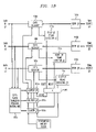
- FIG. 1B shows an alternative implementation of the embodiment shown in FIG. 1A wherein a single highly over-sampled oscillator includes a digital division scheme to individually control the division of a single master clock with respect to each of a plurality of received data streams, in accordance with the principles of the present invention.
- FIG. 2 shows a TDMA burst including less than all data frames including a sync word, and remaining data frames toward the end of the TDMA burst including a data payload field 0 in place of a sync word, in accordance with the principles of the present invention.
- FIG. 3A shows an ideal positioning of transitions of a data clock (waveform (b)) with respect to bits or symbols of a received data stream (waveform (a)).
- FIG. 3B shows a drifted positioning of transitions of a data clock (waveform (b)) with respect to a last bit or symbol of a received TDMA burst (waveform (a)).
- FIG. 4 shows a plurality of transmitter devices communicating with a receiver device using TDMA frames.
- FIG. 5A shows multiple data frames within a single TDMA burst
- FIG. 5B shows a single data frame in more detail.
- FIG. 6 shows a conventional technique for recovering a data clock from a received TDMA signal.
- FIG. 7 shows the preferred positioning of an active edge of the recovered data clock (waveform (b)) with respect to the positioning of the recovered data (waveform(a)).
- the present invention allows for the elimination or reuse of the portion of TDMA frames otherwise containing the sync word, or even elimination of the bandwidth required to support the increased length of the data frame due to existence of the sync word.
- the sync word is eliminated from the remaining frame structure.
- Drift of a local clock with respect to an incoming data stream is monitored using an oversampled or multiplied master clock to provide suitable resolution to determine an approximate position of an active edge of the master clock with respect to a bit or symbol being clocked. Any drift from center results in an adjustment of the local master clock.
- the drift is measured during a received TDMA burst, and the master clock is adjusted to re-center the local master clock with respect to that last bit so that the transmit and receive master clocks are nearly identical in frequency and phase at the end of the TDMA frame.
- the receiver is ‘tuned’ to the clock signal of the transmitting TDMA device such that the receiving TDMA device can predict where the next start of frame will occur. By doing so, the sync word is no longer necessary in the remaining frames of the TDMA burst to decode the start of next TDMA frame.
- the sync word may be included in one or more frames in the beginning of the TDMA transmission, but is eliminated from one or more frames during the remainder of the TDMA transmission.
- FIG. 1 shows a front end of a receiver including monitoring of a position of the active transition of a master clock with respect to the positioning of the received data, and control of the master clock, in accordance with the principles of the present invention.
- a TDMA receiver front end 100 includes an appropriate receiver 104 (e.g., RF, BLUETOOTHTM, etc.), clocked by a master clock 108 .
- the received TDMA data burst is output to a data recovery module 102 , which is clocked by a data clock signal recovered in an appropriate manner.
- the TDMA receiver front end 100 further includes a data clock transition position determiner 150 which determines the position of the clock transition (e.g., negative edge) with respect to the data bit or symbol which it is clocking.
- the data clock transition position determiner 150 determines whether or not the active edge of the output of the master clock 108 is centered on the recovered data. Any variation from center causes an adjust control signal to the master clock 108 in a feedback control technique.
- the adjust control signal may be digital or analog. Moreover, the adjust control signal may represent, e.g., a voltage level to control a voltage controlled oscillator (VCO) or other clock source in the master clock 108 .
- VCO voltage controlled oscillator
- an oversampled clock or subdivided symbol period clock signal is provided.
- 10% resolution is provided using a times ten ( ⁇ 10) frequency multiplier 160 .
- FIG. 1A shows a front end of a receiver including monitoring of multiple received streams from multiple transmitters, wherein the position of the active transition of a corresponding master clock is adjusted with respect to the positioning of each stream of received data, in accordance with the principles of the present invention.
- a separate receive oscillator/master clock may be implemented for each received TDMA data stream received from different transmitters.
- a corresponding master clock is assigned to a particular received TDMA data stream from a particular transmitter. All received TDMA data streams are assigned to individual master clocks.
- the corresponding master clock for that particular TDMA data stream from that particular transmitter is adjusted, and monitored, otherwise in accordance with the principles of the present invention shown and described with respect to FIG. 1 .
- FIG. 1B shows an alternative implementation of the embodiment shown in FIG. 1A wherein a single highly over-sampled oscillator includes a digital division scheme to individually control the division of a single master clock with respect to each of a plurality of received data streams, in accordance with the principles of the present invention.
- a single highly oversampled master clock is used to produce a desirable clock signal to respective data recovery circuits 102 a – 102 c , after appropriate adjustment by a digital divider 191 .
- the digital divider 191 suitably divides the highly oversampled master clock to arrive at a desired frequency and phase for the corresponding data recovery circuit 102 a – 102 c .
- the division performed by the digital divider 191 is occasionally, periodically, or otherwise checked for accuracy and precision from time to time, and appropriately adjusted for each received TDMA data signal from different transmitters.
- FIG. 2 shows a TDMA burst including less than all data frames including a sync word, and remaining data frames toward the end of the TDMA burst including a data payload field zero (field 0 ) in place of a sync word, in accordance with the principles of the present invention.
- a TDMA burst 200 includes a plurality of data frames 202 – 208 .
- the initial one or so frames 202 , 204 include a sync word 210 .
- the sync word may be removed or replaced for the remaining frames 206 , 208 .
- the sync word which otherwise would be present in the last frames 206 , 208 is replaced with a data payload field (e.g., fld. 0 ).
- the sync word may be eliminated, shortening the remaining data frames and thus reducing the bandwidth required to transmit the TDMA burst.
- the sync word may be inserted periodically into data frames, but not into all data frames, and preferably not into a majority of data frames. For example, the sync word may be inserted into every 100 th data frame.
- FIG. 3A shows an ideal positioning of transitions of a data clock (waveform (b)) with respect to bits or symbols of a received data stream (waveform (a)).
- the active edge of the master clock 108 (waveform (a)) is ideally centered with respect to the received data (waveform (b)). This centering is ensured by the control loop formed by the data clock transition position determiner 150 and control of the master clock 108 .
- This control loop insures that when the TDMA burst receiver front end 100 turns on, it will always start in the middle of a certain incoming symbol in a TDMA frame, for example during the first symbol in a preamble sequence.
- a timing recovery circuit associated with the master clock 108 is then allowed to update based on symbol transitions of the incoming frame for the duration of the frame.
- FIG. 3B shows a drifted positioning of transitions of a data clock (waveform (b)) with respect to a last bit or symbol of a received TDMA burst (waveform (a)).
- the positioning of the recovered clock output (waveform (b)) may inevitably tend to drift from the beginning of the TDMA burst toward the end of the TDMA burst.
- the active edge (e.g., negative edge) of the local master clock 108 is shown to have sped up slightly such that the active transition of the master clock 108 occurs 40% into the data bit, with 60% of the data bit remaining after the active transition of the master clock 108 .
- the shift of the master clock 108 is measured by the data clock transition position determiner 150 , which utilizes an oversampled or faster clock (e.g., the master clock multiplied by ten as shown in waveform (c)).
- an oversampled or faster clock e.g., the master clock multiplied by ten as shown in waveform (c)
- the jitter of the local clock and control timing in terms of receiver turn on time are controlled to within less than one symbol time so that a symbol boundary is not crossed from frame to frame. This is particularly desirable in terms of when the receiver is turned on relative to where the first incoming symbol is positioned with respect to the active edge of the master clock.
- a control loop monitors the state of timing recovery at the end of the TDMA burst to see if the local master clock has drifted off from the center of the last symbol at the end of the burst. If so, an adjustment to the local master oscillator 108 is made to bring it back towards the center of the first symbol in the next incoming TDMA burst.
- the first and last symbol of each frame may be effectively wasted since only half of the symbol time may be fed into the receiver. Typically, this is not sufficient energy integration time to make a correct symbol decision. However, since first and last symbols are normally considered not reliable, and since a sync word is usually several bits in length, a net gain remains by removing or replacing the sync word altogether.
- the described embodiments can be implemented in, e.g., a cordless telephone chipset using a non-coherent FSK integrate and dump receiver.
- the receiver oscillator or clock control loop may be implemented in, e.g., software.
- the present invention provides improved performance in terms of link quality, as compared to conventional sync word detection based schemes.
- the present invention eliminates the need for extra bandwidth to carry the non-payload type information associated with the conventional use of a sync word.
- the present invention also improves link performance.
Landscapes
- Engineering & Computer Science (AREA)
- Computer Networks & Wireless Communication (AREA)
- Signal Processing (AREA)
- Synchronisation In Digital Transmission Systems (AREA)
- Time-Division Multiplex Systems (AREA)
Abstract
Description
Claims (14)
Priority Applications (1)
| Application Number | Priority Date | Filing Date | Title |
|---|---|---|---|
| US09/817,054 US7242696B2 (en) | 2001-03-27 | 2001-03-27 | Digital TDMA link with no sync word |
Applications Claiming Priority (1)
| Application Number | Priority Date | Filing Date | Title |
|---|---|---|---|
| US09/817,054 US7242696B2 (en) | 2001-03-27 | 2001-03-27 | Digital TDMA link with no sync word |
Publications (2)
| Publication Number | Publication Date |
|---|---|
| US20020141434A1 US20020141434A1 (en) | 2002-10-03 |
| US7242696B2 true US7242696B2 (en) | 2007-07-10 |
Family
ID=25222257
Family Applications (1)
| Application Number | Title | Priority Date | Filing Date |
|---|---|---|---|
| US09/817,054 Expired - Fee Related US7242696B2 (en) | 2001-03-27 | 2001-03-27 | Digital TDMA link with no sync word |
Country Status (1)
| Country | Link |
|---|---|
| US (1) | US7242696B2 (en) |
Cited By (3)
| Publication number | Priority date | Publication date | Assignee | Title |
|---|---|---|---|---|
| US20060268832A1 (en) * | 2005-05-26 | 2006-11-30 | Cisco Technology, Inc. | Transporting synchronization channel information across a packet network |
| US20070126610A1 (en) * | 2003-10-13 | 2007-06-07 | Kahlman Josephus Arnoldus H M | Balanced disparity frame sync |
| US20090080498A1 (en) * | 2007-09-24 | 2009-03-26 | Deisher Michael E | Adaptive radio frequency interference mitigation during channel scanning or hopping |
Families Citing this family (3)
| Publication number | Priority date | Publication date | Assignee | Title |
|---|---|---|---|---|
| US9635540B2 (en) | 2002-03-25 | 2017-04-25 | Jeffrey D. Mullen | Systems and methods for locating cellular phones and security measures for the same |
| EP1916789B1 (en) * | 2006-10-23 | 2009-02-11 | Alcatel Lucent | Synchronization method and synchronization system |
| US11231740B2 (en) * | 2019-02-06 | 2022-01-25 | Credo Technology Group Limited | Clock recovery using between-interval timing error estimation |
Citations (10)
| Publication number | Priority date | Publication date | Assignee | Title |
|---|---|---|---|---|
| US3724139A (en) * | 1971-06-11 | 1973-04-03 | Gehl Co | Blade sharpening device for rotatable chopping cylinders |
| US4316284A (en) * | 1980-09-11 | 1982-02-16 | Bell Telephone Laboratories, Incorporated | Frame resynchronization circuit for digital receiver |
| US5235598A (en) * | 1992-01-30 | 1993-08-10 | Motorola, Inc. | Method for utilizing a control channel for both data and voice |
| US5282226A (en) * | 1992-04-27 | 1994-01-25 | Hughes Aircraft Company | System and method for transmission of bursts of digital information |
| US5325405A (en) * | 1991-08-27 | 1994-06-28 | Motorola, Inc. | Burst mode receiver control |
| US5566210A (en) * | 1993-11-29 | 1996-10-15 | Matsushita Electric Industrial Co., Ltd. | Data receiving apparatus |
| US5886999A (en) * | 1994-02-28 | 1999-03-23 | Fujitsu Limited | Receiving apparatus and method of outputting received signal in multimedia communication |
| US5920547A (en) * | 1996-07-24 | 1999-07-06 | Nokia Mobile Phones, Limited | TDD method between a base station and at least one mobile station |
| US5960046A (en) * | 1996-12-03 | 1999-09-28 | Northern Telecom Limited | Preamble based selection diversity in a time division multiple access radio system |
| US6111927A (en) * | 1996-07-11 | 2000-08-29 | Nokia Mobile Phones Limited | Method and apparatus for resynchronizing two system clocks |
-
2001
- 2001-03-27 US US09/817,054 patent/US7242696B2/en not_active Expired - Fee Related
Patent Citations (10)
| Publication number | Priority date | Publication date | Assignee | Title |
|---|---|---|---|---|
| US3724139A (en) * | 1971-06-11 | 1973-04-03 | Gehl Co | Blade sharpening device for rotatable chopping cylinders |
| US4316284A (en) * | 1980-09-11 | 1982-02-16 | Bell Telephone Laboratories, Incorporated | Frame resynchronization circuit for digital receiver |
| US5325405A (en) * | 1991-08-27 | 1994-06-28 | Motorola, Inc. | Burst mode receiver control |
| US5235598A (en) * | 1992-01-30 | 1993-08-10 | Motorola, Inc. | Method for utilizing a control channel for both data and voice |
| US5282226A (en) * | 1992-04-27 | 1994-01-25 | Hughes Aircraft Company | System and method for transmission of bursts of digital information |
| US5566210A (en) * | 1993-11-29 | 1996-10-15 | Matsushita Electric Industrial Co., Ltd. | Data receiving apparatus |
| US5886999A (en) * | 1994-02-28 | 1999-03-23 | Fujitsu Limited | Receiving apparatus and method of outputting received signal in multimedia communication |
| US6111927A (en) * | 1996-07-11 | 2000-08-29 | Nokia Mobile Phones Limited | Method and apparatus for resynchronizing two system clocks |
| US5920547A (en) * | 1996-07-24 | 1999-07-06 | Nokia Mobile Phones, Limited | TDD method between a base station and at least one mobile station |
| US5960046A (en) * | 1996-12-03 | 1999-09-28 | Northern Telecom Limited | Preamble based selection diversity in a time division multiple access radio system |
Cited By (7)
| Publication number | Priority date | Publication date | Assignee | Title |
|---|---|---|---|---|
| US20070126610A1 (en) * | 2003-10-13 | 2007-06-07 | Kahlman Josephus Arnoldus H M | Balanced disparity frame sync |
| US7852238B2 (en) * | 2003-10-13 | 2010-12-14 | Koninklijke Philips Electronics N.V. | Balanced disparity frame sync |
| US20060268832A1 (en) * | 2005-05-26 | 2006-11-30 | Cisco Technology, Inc. | Transporting synchronization channel information across a packet network |
| US7627004B2 (en) * | 2005-05-26 | 2009-12-01 | Cisco Technology, Inc. | Transporting synchronization channel information across a packet network |
| US20090080498A1 (en) * | 2007-09-24 | 2009-03-26 | Deisher Michael E | Adaptive radio frequency interference mitigation during channel scanning or hopping |
| US8625655B2 (en) | 2007-09-24 | 2014-01-07 | Intel Corporation | Adaptive radio frequency interference mitigation during channel scanning or hopping |
| CN101803218B (en) * | 2007-09-24 | 2014-06-11 | 英特尔公司 | Adaptive radio frequency interference mitigation during channel scanning or hopping |
Also Published As
| Publication number | Publication date |
|---|---|
| US20020141434A1 (en) | 2002-10-03 |
Similar Documents
| Publication | Publication Date | Title |
|---|---|---|
| US6970448B1 (en) | Wireless TDMA system and method for network communications | |
| US8306071B2 (en) | Method for selecting an operating mode based on a detected synchornization pattern | |
| US6243372B1 (en) | Methods and apparatus for synchronization in a wireless network | |
| US20120307949A1 (en) | Burst Mode Clock and Data Recovery Circuit and Method | |
| US8416902B2 (en) | Clock and data recovery for burst-mode serial signals | |
| US9966994B2 (en) | Apparatus and methods for burst mode clock and data recovery for high speed serial communication links | |
| US6275517B1 (en) | Wireless communication apparatus using frequency hopping, and method of controlling the apparatus | |
| US20080205568A1 (en) | Dsrc communication circuit and dsrc communication method | |
| US5436937A (en) | Multi-mode digital phase lock loop | |
| US7474723B2 (en) | DSRC communication circuit and communication method | |
| JP2595602B2 (en) | Satellite communication earth station transmission / reception method | |
| US7242696B2 (en) | Digital TDMA link with no sync word | |
| KR101085741B1 (en) | Inter-station transmission method and monitoring method of radio base station and apparatus using the method | |
| KR100965192B1 (en) | Fast timing capture for multiple wireless handsets | |
| US20210195662A1 (en) | Information processing device, information processing method, transmitter, transmission method, receiver, reception method | |
| US7027535B1 (en) | Frequency tracking loop and method of frequency tracking | |
| EP1478119B1 (en) | Method of recovering clock signal using user clock code in TDM digital video signal and transmitting/receiving apparatus user for the method | |
| JP2000315991A (en) | Clock frequency control method and receiver used for it | |
| US7386081B2 (en) | Timing control circuit and method thereof | |
| JP2008010992A (en) | Communication device | |
| JPH1098459A (en) | Clock synchronizing system | |
| HK40061683B (en) | Signalling a multicast message in non-coordinated networks | |
| JPH0530062A (en) | Frame synchronization circuit | |
| JP2001186204A (en) | Digital radio | |
| JPH03286630A (en) | Clock synchronizing system |
Legal Events
| Date | Code | Title | Description |
|---|---|---|---|
| AS | Assignment |
Owner name: AGERE SYSTEMS GUARDIAN CORP., FLORIDA Free format text: ASSIGNMENT OF ASSIGNORS INTEREST;ASSIGNORS:GRUNDVIG, JEFFREY P.;YUAN, YUN XIANG;REEL/FRAME:011661/0983;SIGNING DATES FROM 20010319 TO 20010324 |
|
| STCF | Information on status: patent grant |
Free format text: PATENTED CASE |
|
| FPAY | Fee payment |
Year of fee payment: 4 |
|
| AS | Assignment |
Owner name: DEUTSCHE BANK AG NEW YORK BRANCH, AS COLLATERAL AG Free format text: PATENT SECURITY AGREEMENT;ASSIGNORS:LSI CORPORATION;AGERE SYSTEMS LLC;REEL/FRAME:032856/0031 Effective date: 20140506 Owner name: DEUTSCHE BANK AG NEW YORK BRANCH, AS COLLATERAL AGENT, NEW YORK Free format text: PATENT SECURITY AGREEMENT;ASSIGNORS:LSI CORPORATION;AGERE SYSTEMS LLC;REEL/FRAME:032856/0031 Effective date: 20140506 |
|
| FPAY | Fee payment |
Year of fee payment: 8 |
|
| AS | Assignment |
Owner name: AVAGO TECHNOLOGIES GENERAL IP (SINGAPORE) PTE. LTD., SINGAPORE Free format text: ASSIGNMENT OF ASSIGNORS INTEREST;ASSIGNOR:AGERE SYSTEMS LLC;REEL/FRAME:035365/0634 Effective date: 20140804 Owner name: AVAGO TECHNOLOGIES GENERAL IP (SINGAPORE) PTE. LTD Free format text: ASSIGNMENT OF ASSIGNORS INTEREST;ASSIGNOR:AGERE SYSTEMS LLC;REEL/FRAME:035365/0634 Effective date: 20140804 |
|
| AS | Assignment |
Owner name: LSI CORPORATION, CALIFORNIA Free format text: TERMINATION AND RELEASE OF SECURITY INTEREST IN PATENT RIGHTS (RELEASES RF 032856-0031);ASSIGNOR:DEUTSCHE BANK AG NEW YORK BRANCH, AS COLLATERAL AGENT;REEL/FRAME:037684/0039 Effective date: 20160201 Owner name: AGERE SYSTEMS LLC, PENNSYLVANIA Free format text: TERMINATION AND RELEASE OF SECURITY INTEREST IN PATENT RIGHTS (RELEASES RF 032856-0031);ASSIGNOR:DEUTSCHE BANK AG NEW YORK BRANCH, AS COLLATERAL AGENT;REEL/FRAME:037684/0039 Effective date: 20160201 |
|
| AS | Assignment |
Owner name: BANK OF AMERICA, N.A., AS COLLATERAL AGENT, NORTH CAROLINA Free format text: PATENT SECURITY AGREEMENT;ASSIGNOR:AVAGO TECHNOLOGIES GENERAL IP (SINGAPORE) PTE. LTD.;REEL/FRAME:037808/0001 Effective date: 20160201 Owner name: BANK OF AMERICA, N.A., AS COLLATERAL AGENT, NORTH Free format text: PATENT SECURITY AGREEMENT;ASSIGNOR:AVAGO TECHNOLOGIES GENERAL IP (SINGAPORE) PTE. LTD.;REEL/FRAME:037808/0001 Effective date: 20160201 |
|
| AS | Assignment |
Owner name: AVAGO TECHNOLOGIES GENERAL IP (SINGAPORE) PTE. LTD., SINGAPORE Free format text: TERMINATION AND RELEASE OF SECURITY INTEREST IN PATENTS;ASSIGNOR:BANK OF AMERICA, N.A., AS COLLATERAL AGENT;REEL/FRAME:041710/0001 Effective date: 20170119 Owner name: AVAGO TECHNOLOGIES GENERAL IP (SINGAPORE) PTE. LTD Free format text: TERMINATION AND RELEASE OF SECURITY INTEREST IN PATENTS;ASSIGNOR:BANK OF AMERICA, N.A., AS COLLATERAL AGENT;REEL/FRAME:041710/0001 Effective date: 20170119 |
|
| AS | Assignment |
Owner name: AVAGO TECHNOLOGIES INTERNATIONAL SALES PTE. LIMITED, SINGAPORE Free format text: MERGER;ASSIGNOR:AVAGO TECHNOLOGIES GENERAL IP (SINGAPORE) PTE. LTD.;REEL/FRAME:047196/0097 Effective date: 20180509 Owner name: AVAGO TECHNOLOGIES INTERNATIONAL SALES PTE. LIMITE Free format text: MERGER;ASSIGNOR:AVAGO TECHNOLOGIES GENERAL IP (SINGAPORE) PTE. LTD.;REEL/FRAME:047196/0097 Effective date: 20180509 |
|
| FEPP | Fee payment procedure |
Free format text: MAINTENANCE FEE REMINDER MAILED (ORIGINAL EVENT CODE: REM.); ENTITY STATUS OF PATENT OWNER: LARGE ENTITY |
|
| AS | Assignment |
Owner name: AVAGO TECHNOLOGIES INTERNATIONAL SALES PTE. LIMITE Free format text: CORRECTIVE ASSIGNMENT TO CORRECT THE EXECUTION DATE PREVIOUSLY RECORDED AT REEL: 047196 FRAME: 0097. ASSIGNOR(S) HEREBY CONFIRMS THE MERGER;ASSIGNOR:AVAGO TECHNOLOGIES GENERAL IP (SINGAPORE) PTE. LTD.;REEL/FRAME:048555/0510 Effective date: 20180905 Owner name: AVAGO TECHNOLOGIES INTERNATIONAL SALES PTE. LIMITED, SINGAPORE Free format text: CORRECTIVE ASSIGNMENT TO CORRECT THE EXECUTION DATE PREVIOUSLY RECORDED AT REEL: 047196 FRAME: 0097. ASSIGNOR(S) HEREBY CONFIRMS THE MERGER;ASSIGNOR:AVAGO TECHNOLOGIES GENERAL IP (SINGAPORE) PTE. LTD.;REEL/FRAME:048555/0510 Effective date: 20180905 |
|
| LAPS | Lapse for failure to pay maintenance fees |
Free format text: PATENT EXPIRED FOR FAILURE TO PAY MAINTENANCE FEES (ORIGINAL EVENT CODE: EXP.); ENTITY STATUS OF PATENT OWNER: LARGE ENTITY |
|
| STCH | Information on status: patent discontinuation |
Free format text: PATENT EXPIRED DUE TO NONPAYMENT OF MAINTENANCE FEES UNDER 37 CFR 1.362 |
|
| FP | Lapsed due to failure to pay maintenance fee |
Effective date: 20190710 |