US7241706B2 - Low k ILD layer with a hydrophilic portion - Google Patents
Low k ILD layer with a hydrophilic portion Download PDFInfo
- Publication number
- US7241706B2 US7241706B2 US10/944,358 US94435804A US7241706B2 US 7241706 B2 US7241706 B2 US 7241706B2 US 94435804 A US94435804 A US 94435804A US 7241706 B2 US7241706 B2 US 7241706B2
- Authority
- US
- United States
- Prior art keywords
- dielectric layer
- layer
- interlayer dielectric
- hydrophilic
- carbon
- Prior art date
- Legal status (The legal status is an assumption and is not a legal conclusion. Google has not performed a legal analysis and makes no representation as to the accuracy of the status listed.)
- Expired - Fee Related, expires
Links
- 239000010410 layer Substances 0.000 claims description 202
- OKTJSMMVPCPJKN-UHFFFAOYSA-N Carbon Chemical compound [C] OKTJSMMVPCPJKN-UHFFFAOYSA-N 0.000 claims description 46
- 229910052799 carbon Inorganic materials 0.000 claims description 46
- 239000000758 substrate Substances 0.000 claims description 39
- 239000011229 interlayer Substances 0.000 claims description 29
- 238000000034 method Methods 0.000 claims description 27
- 239000000463 material Substances 0.000 claims description 21
- 230000002209 hydrophobic effect Effects 0.000 claims description 18
- 230000005855 radiation Effects 0.000 claims description 17
- XUIMIQQOPSSXEZ-UHFFFAOYSA-N Silicon Chemical compound [Si] XUIMIQQOPSSXEZ-UHFFFAOYSA-N 0.000 claims description 13
- 229910052710 silicon Inorganic materials 0.000 claims description 13
- 239000010703 silicon Substances 0.000 claims description 13
- QVGXLLKOCUKJST-UHFFFAOYSA-N atomic oxygen Chemical compound [O] QVGXLLKOCUKJST-UHFFFAOYSA-N 0.000 claims description 11
- 230000005670 electromagnetic radiation Effects 0.000 claims description 11
- 229910052760 oxygen Inorganic materials 0.000 claims description 11
- 239000001301 oxygen Substances 0.000 claims description 11
- 229910017052 cobalt Inorganic materials 0.000 claims description 5
- 239000010941 cobalt Substances 0.000 claims description 5
- GUTLYIVDDKVIGB-UHFFFAOYSA-N cobalt atom Chemical compound [Co] GUTLYIVDDKVIGB-UHFFFAOYSA-N 0.000 claims description 5
- 238000000151 deposition Methods 0.000 claims description 5
- 238000007772 electroless plating Methods 0.000 claims description 2
- 239000011203 carbon fibre reinforced carbon Substances 0.000 claims 1
- 229910018557 Si O Inorganic materials 0.000 abstract description 10
- LIVNPJMFVYWSIS-UHFFFAOYSA-N silicon monoxide Inorganic materials [Si-]#[O+] LIVNPJMFVYWSIS-UHFFFAOYSA-N 0.000 abstract description 10
- 229910018540 Si C Inorganic materials 0.000 abstract description 8
- 229910010271 silicon carbide Inorganic materials 0.000 abstract description 8
- 239000004020 conductor Substances 0.000 description 8
- 230000015572 biosynthetic process Effects 0.000 description 5
- XLYOFNOQVPJJNP-UHFFFAOYSA-N water Substances O XLYOFNOQVPJJNP-UHFFFAOYSA-N 0.000 description 3
- VYPSYNLAJGMNEJ-UHFFFAOYSA-N Silicium dioxide Chemical compound O=[Si]=O VYPSYNLAJGMNEJ-UHFFFAOYSA-N 0.000 description 2
- 230000004888 barrier function Effects 0.000 description 2
- 239000011324 bead Substances 0.000 description 2
- 239000003989 dielectric material Substances 0.000 description 2
- 238000004377 microelectronic Methods 0.000 description 2
- RYGMFSIKBFXOCR-UHFFFAOYSA-N Copper Chemical compound [Cu] RYGMFSIKBFXOCR-UHFFFAOYSA-N 0.000 description 1
- UFHFLCQGNIYNRP-UHFFFAOYSA-N Hydrogen Chemical compound [H][H] UFHFLCQGNIYNRP-UHFFFAOYSA-N 0.000 description 1
- 229910008051 Si-OH Inorganic materials 0.000 description 1
- 229910008284 Si—F Inorganic materials 0.000 description 1
- 229910006358 Si—OH Inorganic materials 0.000 description 1
- XAGFODPZIPBFFR-UHFFFAOYSA-N aluminium Chemical compound [Al] XAGFODPZIPBFFR-UHFFFAOYSA-N 0.000 description 1
- 229910052782 aluminium Inorganic materials 0.000 description 1
- 239000003990 capacitor Substances 0.000 description 1
- 229910052681 coesite Inorganic materials 0.000 description 1
- 229910052802 copper Inorganic materials 0.000 description 1
- 239000010949 copper Substances 0.000 description 1
- 229910052906 cristobalite Inorganic materials 0.000 description 1
- 230000001419 dependent effect Effects 0.000 description 1
- 238000009792 diffusion process Methods 0.000 description 1
- 238000005530 etching Methods 0.000 description 1
- 229910052739 hydrogen Inorganic materials 0.000 description 1
- 239000001257 hydrogen Substances 0.000 description 1
- 230000005660 hydrophilic surface Effects 0.000 description 1
- 239000011810 insulating material Substances 0.000 description 1
- 239000007788 liquid Substances 0.000 description 1
- 238000012986 modification Methods 0.000 description 1
- 230000004048 modification Effects 0.000 description 1
- 230000006855 networking Effects 0.000 description 1
- 238000004806 packaging method and process Methods 0.000 description 1
- 229920002120 photoresistant polymer Polymers 0.000 description 1
- 238000005498 polishing Methods 0.000 description 1
- 239000004065 semiconductor Substances 0.000 description 1
- 239000000377 silicon dioxide Substances 0.000 description 1
- 239000002356 single layer Substances 0.000 description 1
- 229910052682 stishovite Inorganic materials 0.000 description 1
- 239000000126 substance Substances 0.000 description 1
- 238000006467 substitution reaction Methods 0.000 description 1
- 229910052905 tridymite Inorganic materials 0.000 description 1
Images


Classifications
-
- H—ELECTRICITY
- H01—ELECTRIC ELEMENTS
- H01L—SEMICONDUCTOR DEVICES NOT COVERED BY CLASS H10
- H01L21/00—Processes or apparatus adapted for the manufacture or treatment of semiconductor or solid state devices or of parts thereof
- H01L21/70—Manufacture or treatment of devices consisting of a plurality of solid state components formed in or on a common substrate or of parts thereof; Manufacture of integrated circuit devices or of parts thereof
- H01L21/71—Manufacture of specific parts of devices defined in group H01L21/70
- H01L21/768—Applying interconnections to be used for carrying current between separate components within a device comprising conductors and dielectrics
- H01L21/76801—Applying interconnections to be used for carrying current between separate components within a device comprising conductors and dielectrics characterised by the formation and the after-treatment of the dielectrics, e.g. smoothing
- H01L21/76829—Applying interconnections to be used for carrying current between separate components within a device comprising conductors and dielectrics characterised by the formation and the after-treatment of the dielectrics, e.g. smoothing characterised by the formation of thin functional dielectric layers, e.g. dielectric etch-stop, barrier, capping or liner layers
-
- H—ELECTRICITY
- H01—ELECTRIC ELEMENTS
- H01L—SEMICONDUCTOR DEVICES NOT COVERED BY CLASS H10
- H01L21/00—Processes or apparatus adapted for the manufacture or treatment of semiconductor or solid state devices or of parts thereof
- H01L21/02—Manufacture or treatment of semiconductor devices or of parts thereof
- H01L21/04—Manufacture or treatment of semiconductor devices or of parts thereof the devices having potential barriers, e.g. a PN junction, depletion layer or carrier concentration layer
- H01L21/18—Manufacture or treatment of semiconductor devices or of parts thereof the devices having potential barriers, e.g. a PN junction, depletion layer or carrier concentration layer the devices having semiconductor bodies comprising elements of Group IV of the Periodic Table or AIIIBV compounds with or without impurities, e.g. doping materials
- H01L21/28—Manufacture of electrodes on semiconductor bodies using processes or apparatus not provided for in groups H01L21/20 - H01L21/268
- H01L21/283—Deposition of conductive or insulating materials for electrodes conducting electric current
- H01L21/288—Deposition of conductive or insulating materials for electrodes conducting electric current from a liquid, e.g. electrolytic deposition
-
- H—ELECTRICITY
- H01—ELECTRIC ELEMENTS
- H01L—SEMICONDUCTOR DEVICES NOT COVERED BY CLASS H10
- H01L21/00—Processes or apparatus adapted for the manufacture or treatment of semiconductor or solid state devices or of parts thereof
- H01L21/70—Manufacture or treatment of devices consisting of a plurality of solid state components formed in or on a common substrate or of parts thereof; Manufacture of integrated circuit devices or of parts thereof
- H01L21/71—Manufacture of specific parts of devices defined in group H01L21/70
- H01L21/768—Applying interconnections to be used for carrying current between separate components within a device comprising conductors and dielectrics
- H01L21/76838—Applying interconnections to be used for carrying current between separate components within a device comprising conductors and dielectrics characterised by the formation and the after-treatment of the conductors
- H01L21/76841—Barrier, adhesion or liner layers
- H01L21/76843—Barrier, adhesion or liner layers formed in openings in a dielectric
- H01L21/76849—Barrier, adhesion or liner layers formed in openings in a dielectric the layer being positioned on top of the main fill metal
-
- H—ELECTRICITY
- H01—ELECTRIC ELEMENTS
- H01L—SEMICONDUCTOR DEVICES NOT COVERED BY CLASS H10
- H01L21/00—Processes or apparatus adapted for the manufacture or treatment of semiconductor or solid state devices or of parts thereof
- H01L21/70—Manufacture or treatment of devices consisting of a plurality of solid state components formed in or on a common substrate or of parts thereof; Manufacture of integrated circuit devices or of parts thereof
- H01L21/71—Manufacture of specific parts of devices defined in group H01L21/70
- H01L21/768—Applying interconnections to be used for carrying current between separate components within a device comprising conductors and dielectrics
- H01L21/76838—Applying interconnections to be used for carrying current between separate components within a device comprising conductors and dielectrics characterised by the formation and the after-treatment of the conductors
- H01L21/76841—Barrier, adhesion or liner layers
- H01L21/76871—Layers specifically deposited to enhance or enable the nucleation of further layers, i.e. seed layers
- H01L21/76874—Layers specifically deposited to enhance or enable the nucleation of further layers, i.e. seed layers for electroless plating
Definitions
- conductors such as vias and traces, carry signals between layers of the substrate or other structure.
- the vias and traces by layers of dielectric materials.
- Low dielectric constant (“k value”) materials are used in the layers of dielectric materials between the conductors to reduce resistance capacitance (“RC”) delay and improve device performance.
- a capping layer such as an electrolessly-plated cobalt capping layer may be formed on the top of such conductors to help minimize issues such as electromigration.
- Such an electroless layer can be formed using a water-based solution that includes the cobalt or other material that may form the capping layer.
- some low-k materials used are hydrophobic, which may make formation of such an electroless layer difficult.
- FIGS. 1 a through 1 e are cross sectional side views that illustrate how a hydrophilic portion of a low k dielectric layer may be formed.
- FIG. 2 illustrates a system that may be used to form a hydrophilic layer out of a portion of the dielectric layer.
- FIG. 3 illustrates a system in accordance with one embodiment.
- FIG. 1 a is a side cross sectional view of a substrate 102 on which a dielectric layer with a low dielectric constant (“k value”), conductive layers such as vias and/or traces, and a capping layer may be formed, according to one embodiment of the present invention.
- the substrate 102 may comprise a piece of material, such as a piece of silicon or other material.
- the substrate 102 may be any surface generated by processing, and may comprise, for example, active and passive devices that are formed on a silicon wafer, such as transistors, capacitors, resistors, local interconnects, and others.
- the substrate 102 may be a physical structure, a layer that is a basic workpiece transformed and/or added to by various processes into the desired microelectronic configuration, or another material or materials.
- the substrate 102 may include conducting material, insulating material, semiconducting material, and other materials or material combinations. In some embodiments, the substrate 102 may be a multi-layered structure.
- the substrate 102 may be a partially complete microprocessor die, with multiple transistors.
- ILD interlayer dielectric
- the substrate 102 may be another type of structure.
- FIG. 1 b is a side cross sectional view of the substrate 102 on which a dielectric layer 104 has been formed, according to one embodiment.
- the dielectric layer 104 may be an ILD layer that will separate conductive interconnects that connect devices of a microprocessor die with other components, such as packaging substrates. In other embodiments, the dielectric layer 104 may serve a different purpose.
- the dielectric layer 104 may be a low-k dielectric layer.
- the k value of the dielectric layer 104 may be below 3.2.
- the k value may be below 3.0.
- the k value may be between about 3.0 and about 2.4. In yet other embodiments, the k value may be different.
- the dielectric layer 104 may include one or more of carbon, silicon, and/or oxygen.
- the layer 104 may also include hydrogen.
- the dielectric layer 104 may include 10% to 75% carbon, with oxygen and silicon.
- the composition of the dielectric layer 104 may be relatively consistent throughout the layer 104 , from the bottom (nearer to the substrate 102 ) to the top (further from the substrate 102 ). Thus, there may be about the same percentage or ratio of carbon/silicon/oxygen in a sample of material taken from the bottom of the dielectric layer 104 as would be in a sample taken from the top of the layer 104 .
- the ratios of Si—C and/or C—C bonds to Si—O bonds may be fairly consistent throughout the dielectric layer 104 ; the ratio of Si—C bonds to Si—O bonds at the bottom of the layer 104 may be similar to the ratio of Si—C bonds to Si—O bonds at the top of the layer 104 .
- the dielectric layer 104 may be relatively hydrophobic. Water and/or water-based solutions may have a tendency to form discrete beads on the surface of the dielectric layer 104 rather than spread out and evenly cover the surface. The presence of SiOC and/or SiCH 3 in the dielectric layer 104 , which may help make the dielectric layer 104 low k, may also make the dielectric layer 104 hydrophobic.
- the dielectric layer 104 may have a thickness 114 of less than about 15 microns. In some embodiments, the dielectric layer 104 may have a thickness 114 of less than about 10 microns. In some embodiments, the dielectric layer 104 may have a thickness 114 of less than about 1 micron. In yet other embodiments, the dielectric layer 104 may have a thickness 114 that is greater or less.
- FIG. 1 c is a side cross sectional view of the substrate 102 , the dielectric layer 104 , and conductive traces 106 and a via 108 , which have been formed in the dielectric layer 104 , according to one embodiment. While only two traces 106 and one via 108 are shown, in some embodiments, there may be many more traces 106 and vias 108 .
- the traces 106 and via 108 may comprise any conductive material, including copper, aluminum, or other materials.
- the traces 106 and via 108 may be formed by any suitable method, such as by using a patterned photoresist layer to protect selected portions of the dielectric layer 104 , etching trenches into unprotected portions of the dielectric layer 104 , then depositing conductive material into the trenches. Prior to depositing the conductive material, a barrier layer, seed layer, and/or adhesion layer may be deposited in some embodiments.
- the top of the traces 106 , vias 108 , and dielectric layer 104 may then be planarized to make the top surface of the dielectric layer 104 substantially even with the top of the conductive material that forms the traces 106 and via 108 .
- the top of the traces 106 , vias 108 , and dielectric layer 104 may be planarized by any suitable method, such as by a chemical mechanical polishing (“CMP”) process.
- CMP chemical mechanical polishing
- the structure as shown in FIG. 1 c may be referred to as a “homogeneous dielectric layer” device 120 or “pre-exposure” device 120 because at this point, the dielectric layer 104 may have a substantially consistent composition throughout, as described above, and the exposure process described below has not yet occurred.
- FIG. 1 d is a side cross sectional view of the substrate 102 , the dielectric layer 104 , conductive traces 106 and via 108 , after formation of a top portion 110 from a portion of the dielectric layer 104 , according to one embodiment.
- the structure as shown in FIG. 1 d may be referred to as a “heterogeneous dielectric layer” device 150 or “post-exposure” device 150 because at this point, the dielectric layer 104 may no longer have a substantially consistent composition throughout, and the exposure process described below may have been performed.
- the dielectric layer 104 may include a top portion 110 (the top portion being the portion of the dielectric layer 104 furthest from the substrate 102 ) that may have a different composition than the rest of the dielectric layer 104 .
- the top portion 110 may also be considered a top layer 110 .
- the top portion 110 may comprise a material that is hydrophilic compared to the rest of the dielectric layer 104 .
- the top portion 110 may be referred to as a hydrophilic portion 110 or hydrophilic layer 110 .
- the rest of the dielectric layer 104 may be referred to as a hydrophobic portion 112 or hydrophobic layer 112 (since it is hydrophobic relative to the top hydrophilic portion 110 ) or the bottom portion 112 or bottom layer 112 (since it is closer to the substrate 102 ).
- the ratio of Si—C and/or C—C bonds to Si—O bonds may be smaller at the top portion 110 of the dielectric layer 104 than at the bottom portion 112 of the dielectric layer 104 .
- the difference in the amount of carbon between the top 110 and bottom 112 may be chosen to make the top portion 110 hydrophilic enough, while retaining a low capacitance in the dielectric layer 104 .
- the amount of carbon at the top surface of the top portion 110 may be reduced by 5%, 10%, 25%, or another amount over the amount of carbon in the bottom portion 112 .
- the top portion 110 may be more hydrophilic and may have a higher k value than the bottom portion 112 .
- the bottom portion 112 of the dielectric layer 104 may have substantially the same composition as the entire dielectric layer 104 did in the homogeneous dielectric layer device 120 .
- the elements, including carbon, silicon, and oxygen in an embodiment, of the bottom portion may be present in the bottom portion 112 in substantially the same ratios as in dielectric layer 104 of the pre-exposure device 120 , and the elements may be present in the top portion 110 in a ratio that includes relatively less carbon than was in the dielectric layer 104 of the pre-exposure device 120 .
- the top layer 110 may have a depth 116 or thickness 116 that is between about 1% to about 15% of the thickness 114 of the dielectric layer 104 . In an embodiment, top portion 110 may have a thickness 116 of up to half the thickness 114 of the dielectric layer 104 . In an embodiment the top layer 110 may have a thickness 116 that is between about 30 angstroms to about 500 angstroms. In some embodiments, the top layer 110 may have enough thickness 116 to provide a hydrophilic surface on which liquids may be deposited. In yet other embodiments, the top portion 110 may have different thicknesses that may be greater or less than those described above.
- the hydrophilic portion 110 may be a graded portion. That is, while FIG. 1 d shows the hydrophilic portion 110 as a single layer, the top portion may not be homogeneous through its thickness 116 . There may be relatively less carbon at the top of the layer 110 than at the bottom of the layer 110 that is adjacent the hydrophobic portion 112 in an embodiment. In an embodiment, the top of the hydrophilic portion 110 (further from the substrate 102 ) may be more hydrophilic and/or have a higher k value than the bottom 111 of the hydrophilic portion 110 (closer to the substrate 102 ).
- carbon percentage difference may be defined as the difference between the percentage of the composition that is carbon of the homogeneous dielectric layer device 120 (and/or of the portion of the dielectric layer near the substrate 102 , which may be the same percentage) and the percentage of the composition that is carbon at a given point where the difference is to be measured.
- the hydrophilic portion 110 is a graded layer
- the bottom 111 of the hydrophilic portion 110 may be defined as the position where the carbon percentage difference is less than 10% than the carbon percentage difference of the top of the top layer 110 .
- FIG. 1 e is a side cross sectional view of the substrate 102 , the dielectric layer 104 , conductive traces 106 and via 108 , and the top hydrophilic layer 110 , after formation of a cap layer 118 on the traces 106 , according to one embodiment.
- the cap layer 118 may be a thin conductive layer that may act as a barrier layer to prevent diffusion or electromigration of the material of the traces 106 .
- the cap layer 118 may comprise cobalt, although it may comprise other materials in other embodiments.
- the cap layer 118 may be an electroless cap layer 118 , or may be formed by other suitable methods.
- the hydrophilic top layer 110 of the dielectric layer 104 may help the electroless solution contact the entire surface, rather than form beads which may result in an uneven or partially formed cap layer 118 .
- the cap layer 118 After formation of the cap layer 118 , there may be further processing performed. For example, one or more additional dielectric layers, each with traces and vias may be formed on the dielectric layer 104 and traces 106 . One or all of such additional dielectric layers may have a top hydrophilic portion formed out of part of the dielectric layer, and cap layers may be formed on the traces in the additional dielectric layers. There may be similar dielectric layers with hydrophilic portions and traces as part of the substrate 102 as well.
- FIG. 2 illustrates a system 200 that may be used to form the hydrophilic layer 110 out of a portion of the dielectric layer 104 .
- the system 200 may include a chamber 202 in which the pre-exposure device 120 , with its substantially homogeneous dielectric layer 104 may be positioned.
- the system 200 may include a vacuum source 208 , which may operate to form a partial vacuum within the chamber 202 .
- the system 200 may also include a radiation source 204 , which may produce and/or direct electromagnetic radiation 206 at the dielectric layer 104 of the pre-exposure device 120 to turn it into the post-exposure device 150 .
- the radiation source 204 generates ultraviolet light 206 that is directed at the pre-exposure device 120 .
- the dielectric layer 104 is thus exposed to the electromagnetic radiation 206 .
- ultraviolet radiation 206 with a wavelength of about 172 nanometers may be directed to the dielectric layer 104 in an embodiment.
- This radiation 206 may have an energy level of about 9.75 eV (about 699 kJ/mole at 298 K).
- Such radiation 206 may have enough energy to break Si—C bonds, which have a bond strength of about 451.5 kJ/mole, and C—C bonds, which have a bond strength of about 610 kJ/mole.
- Si—O bonds with a bond strength of about 799.6 kJ/mole tend not to be broken by such radiation 206 . This may result in the bonds between carbon and other elements at the top the dielectric layer 104 (the portion of the dielectric layer 104 that is struck by the radiation 206 ) being broken and the carbon leaving the dielectric layer 104 to the surrounding environment. This may result in less carbon and relatively more Si—O being present in the top portion 110 of the dielectric layer 104 , which may result in the top portion 110 of the dielectric layer 104 becoming more hydrophilic than the bottom portion 112 of the dielectric layer 104 .
- bonds may be selectively broken at a top portion 110 of the dielectric layer 104 to form a relatively hydrophilic portion 110 .
- Si—CH 3 bonds with a bond strength of about 283 kJ/mole
- Si—H bonds with a bond strength of about 299 kJ/mole
- Si—O bonds may be selectively broken, leaving Si—O bonds relatively unaffected. Since Si—CH 3 and Si—H are relatively hydrophobic and Si—O is relatively hydrophilic, such a situation would make the top portion 110 more hydrophilic.
- a wavelength of radiation 206 and other process conditions may be chosen to selectively break bonds.
- Some additional bond strength values are as follows: C—O bonds, with a bond strength of about 1077 kJ/mole, C—N bonds, with a bond strength of about 754 kJ/mole, Si—OH bonds, with a bond strength of about 483 kJ/mole, Si—CH 2 bonds, with a bond strength of about 527 kJ/mole, Si—CH bonds, with a bond strength of about 543 kJ/mole, and Si—F bonds, with a bond strength of about 553 kJ/mole.
- the wavelength of the radiation 206 may be different than 172 nanometers.
- the wavelength of the radiation 206 may be chosen to have enough energy to break Si—C and C—C bonds but not enough to break Si—O bonds.
- the radiation 206 used may have a wavelength between about 160 nanometers and about 275 nanometers, although other wavelengths may also be used.
- the pre-exposure device 120 may be exposed to radiation 206 for less than about 45 seconds, although different times may be used. Each of the wavelength and exposure time may affect the depth 116 of the top portion 110 , and the amount of carbon removed from the top surface of the dielectric layer 104 .
- the depth 116 and amount of carbon removed may be controlled by selecting a wavelength.
- the pre-exposure device 120 may be exposed to radiation 206 at a temperature below about 400 degrees Celsius.
- the temperature at which the pre-exposure device 120 is exposed to radiation 206 may be chosen based on the type of material that comprises the dielectric layer 104 .
- an organic dielectric layer 104 may be exposed to radiation 206 at a lower temperature than a carbon doped oxide dielectric layer 104 .
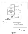
- FIG. 3 illustrates a system 300 in accordance with one embodiment.
- system 300 includes computing device 302 for processing data.
- Computing device 302 may include a motherboard 304 .
- Motherboard 304 may include in particular a processor 306 , and a networking interface 308 coupled to a bus 310 .
- the substrate 102 and dielectric layer 104 with the hydrophilic portion 110 described above may comprise part of the processor 306 .
- the die 306 may be attached to a package substrate, which may then be attached to the motherboard 304 .
- system 300 may include other components, including but are not limited to volatile and non-volatile memory 312 , a graphics processor, a digital signal processor, a crypto processor, a chipset, mass storage 314 (such as hard disk, compact disk (CD), digital versatile disk (DVD) and so forth), input and/or output devices 316 , and so forth.
- volatile and non-volatile memory 312 a graphics processor, a digital signal processor, a crypto processor, a chipset, mass storage 314 (such as hard disk, compact disk (CD), digital versatile disk (DVD) and so forth), input and/or output devices 316 , and so forth.
- mass storage 314 such as hard disk, compact disk (CD), digital versatile disk (DVD) and so forth
- input and/or output devices 316 input and/or output devices 316 , and so forth.
- One or more of these components may also include the earlier described dielectric layer 104 with the hydrophilic portion 110 .
- system 300 may be a personal digital assistant (PDA), a mobile phone, a tablet computing device, a laptop computing device, a desktop computing device, a set-top box, an entertainment control unit, a digital camera, a digital video recorder, a CD player, a DVD player, or other digital device of the like.
- PDA personal digital assistant
Landscapes
- Engineering & Computer Science (AREA)
- Physics & Mathematics (AREA)
- Condensed Matter Physics & Semiconductors (AREA)
- General Physics & Mathematics (AREA)
- Manufacturing & Machinery (AREA)
- Computer Hardware Design (AREA)
- Microelectronics & Electronic Packaging (AREA)
- Power Engineering (AREA)
- Internal Circuitry In Semiconductor Integrated Circuit Devices (AREA)
Abstract
Description
Claims (24)
Priority Applications (1)
| Application Number | Priority Date | Filing Date | Title |
|---|---|---|---|
| US10/944,358 US7241706B2 (en) | 2004-09-16 | 2004-09-16 | Low k ILD layer with a hydrophilic portion |
Applications Claiming Priority (1)
| Application Number | Priority Date | Filing Date | Title |
|---|---|---|---|
| US10/944,358 US7241706B2 (en) | 2004-09-16 | 2004-09-16 | Low k ILD layer with a hydrophilic portion |
Publications (2)
| Publication Number | Publication Date |
|---|---|
| US20060057838A1 US20060057838A1 (en) | 2006-03-16 |
| US7241706B2 true US7241706B2 (en) | 2007-07-10 |
Family
ID=36034616
Family Applications (1)
| Application Number | Title | Priority Date | Filing Date |
|---|---|---|---|
| US10/944,358 Expired - Fee Related US7241706B2 (en) | 2004-09-16 | 2004-09-16 | Low k ILD layer with a hydrophilic portion |
Country Status (1)
| Country | Link |
|---|---|
| US (1) | US7241706B2 (en) |
Families Citing this family (1)
| Publication number | Priority date | Publication date | Assignee | Title |
|---|---|---|---|---|
| US20090017624A1 (en) * | 2007-07-09 | 2009-01-15 | Chih-Hung Liao | Nodule Defect Reduction in Electroless Plating |
Citations (4)
| Publication number | Priority date | Publication date | Assignee | Title |
|---|---|---|---|---|
| US6383913B1 (en) * | 2001-04-06 | 2002-05-07 | United Microelectronics Corp. | Method for improving surface wettability of low k material |
| US20030054115A1 (en) * | 2001-09-14 | 2003-03-20 | Ralph Albano | Ultraviolet curing process for porous low-K materials |
| US20030089992A1 (en) * | 1998-10-01 | 2003-05-15 | Sudha Rathi | Silicon carbide deposition for use as a barrier layer and an etch stop |
| US20050042388A1 (en) * | 2002-12-04 | 2005-02-24 | Kazuyuki Mitsuoka | Method of processing an organic-film |
-
2004
- 2004-09-16 US US10/944,358 patent/US7241706B2/en not_active Expired - Fee Related
Patent Citations (4)
| Publication number | Priority date | Publication date | Assignee | Title |
|---|---|---|---|---|
| US20030089992A1 (en) * | 1998-10-01 | 2003-05-15 | Sudha Rathi | Silicon carbide deposition for use as a barrier layer and an etch stop |
| US6383913B1 (en) * | 2001-04-06 | 2002-05-07 | United Microelectronics Corp. | Method for improving surface wettability of low k material |
| US20030054115A1 (en) * | 2001-09-14 | 2003-03-20 | Ralph Albano | Ultraviolet curing process for porous low-K materials |
| US20050042388A1 (en) * | 2002-12-04 | 2005-02-24 | Kazuyuki Mitsuoka | Method of processing an organic-film |
Non-Patent Citations (2)
| Title |
|---|
| Carlo Waldfried et al., "Single Wafer Rapid Curing(TM) of Porous Low-k Materials", IEEE, pp. 226-228. |
| Ronald C. Hedden et al., "Comparison of Curing Processes for Porous Dielectrics Measurements from Specular X-Ray Reflectivity", Journal of the Electrochemical Society, 151 (8) F178-F181 (2004). |
Also Published As
| Publication number | Publication date |
|---|---|
| US20060057838A1 (en) | 2006-03-16 |
Similar Documents
| Publication | Publication Date | Title |
|---|---|---|
| US8872354B2 (en) | Method of forming through silicon via of semiconductor device using low-K dielectric material | |
| KR100888881B1 (en) | Integrated low-k hard mask | |
| KR102073176B1 (en) | Conformal low temperature hermetic dielectric diffusion barriers | |
| US7354862B2 (en) | Thin passivation layer on 3D devices | |
| JP5328111B2 (en) | Interconnect structure with improved adhesion between noble metal liner and dielectric material adjacent to it and its manufacturing method (improved adhesion for metal / dielectric interface) | |
| US8847405B2 (en) | Integrated circuits including air gaps around interconnect structures, and fabrication methods thereof | |
| US20060216929A1 (en) | Etch stopless dual damascene structure and method of fabrication | |
| US9543234B2 (en) | In-situ formation of silicon and tantalum containing barrier | |
| US10079147B2 (en) | Method of forming interconnects for semiconductor devices | |
| US10727114B2 (en) | Interconnect structure including airgaps and substractively etched metal lines | |
| US8338290B2 (en) | Method for fabricating semiconductor device | |
| US7241706B2 (en) | Low k ILD layer with a hydrophilic portion | |
| US7687392B2 (en) | Semiconductor device having metal wiring and method for fabricating the same | |
| CN104425362B (en) | Interconnection structure and forming method thereof | |
| JPWO2004105123A1 (en) | Semiconductor device | |
| US20230178379A1 (en) | Film deposition for patterning process | |
| CN112864003B (en) | Etching method for reducing influence of surface defects | |
| US20230111315A1 (en) | Method for fabricating semiconductor device with plug structure | |
| US20230197602A1 (en) | Staggered vertically spaced integrated circuit line metallization with differential vias & metal-selective deposition | |
| KR100928107B1 (en) | Semiconductor device and manufacturing method thereof | |
| US20080044998A1 (en) | Method of Fabricating Metal Interconnection of Semiconductor Device |
Legal Events
| Date | Code | Title | Description |
|---|---|---|---|
| AS | Assignment |
Owner name: INTEL CORPORATION, CALIFORNIA Free format text: ASSIGNMENT OF ASSIGNORS INTEREST;ASSIGNORS:JOHNSTON, STEVEN W.;BAXTER, NATE;REEL/FRAME:015814/0148 Effective date: 20040819 |
|
| STCF | Information on status: patent grant |
Free format text: PATENTED CASE |
|
| FPAY | Fee payment |
Year of fee payment: 4 |
|
| FEPP | Fee payment procedure |
Free format text: PAYER NUMBER DE-ASSIGNED (ORIGINAL EVENT CODE: RMPN); ENTITY STATUS OF PATENT OWNER: LARGE ENTITY Free format text: PAYOR NUMBER ASSIGNED (ORIGINAL EVENT CODE: ASPN); ENTITY STATUS OF PATENT OWNER: LARGE ENTITY |
|
| FPAY | Fee payment |
Year of fee payment: 8 |
|
| FEPP | Fee payment procedure |
Free format text: MAINTENANCE FEE REMINDER MAILED (ORIGINAL EVENT CODE: REM.); ENTITY STATUS OF PATENT OWNER: LARGE ENTITY |
|
| LAPS | Lapse for failure to pay maintenance fees |
Free format text: PATENT EXPIRED FOR FAILURE TO PAY MAINTENANCE FEES (ORIGINAL EVENT CODE: EXP.); ENTITY STATUS OF PATENT OWNER: LARGE ENTITY |
|
| STCH | Information on status: patent discontinuation |
Free format text: PATENT EXPIRED DUE TO NONPAYMENT OF MAINTENANCE FEES UNDER 37 CFR 1.362 |
|
| FP | Lapsed due to failure to pay maintenance fee |
Effective date: 20190710 |