US7228024B2 - Optical return loss detecting device - Google Patents
Optical return loss detecting device Download PDFInfo
- Publication number
- US7228024B2 US7228024B2 US10/892,117 US89211704A US7228024B2 US 7228024 B2 US7228024 B2 US 7228024B2 US 89211704 A US89211704 A US 89211704A US 7228024 B2 US7228024 B2 US 7228024B2
- Authority
- US
- United States
- Prior art keywords
- optical
- coupler
- return loss
- port
- detecting device
- Prior art date
- Legal status (The legal status is an assumption and is not a legal conclusion. Google has not performed a legal analysis and makes no representation as to the accuracy of the status listed.)
- Expired - Fee Related, expires
Links
Images


Classifications
-
- G—PHYSICS
- G01—MEASURING; TESTING
- G01M—TESTING STATIC OR DYNAMIC BALANCE OF MACHINES OR STRUCTURES; TESTING OF STRUCTURES OR APPARATUS, NOT OTHERWISE PROVIDED FOR
- G01M11/00—Testing of optical apparatus; Testing structures by optical methods not otherwise provided for
- G01M11/30—Testing of optical devices, constituted by fibre optics or optical waveguides
- G01M11/31—Testing of optical devices, constituted by fibre optics or optical waveguides with a light emitter and a light receiver being disposed at the same side of a fibre or waveguide end-face, e.g. reflectometers
- G01M11/3109—Reflectometers detecting the back-scattered light in the time-domain, e.g. OTDR
- G01M11/3154—Details of the opto-mechanical connection, e.g. connector or repeater
Definitions
- the present invention relates to an optical return loss detecting device, particularly to an optical return loss detecting device which is compact and can precisely measure the optical return loss value of optics devices.
- Optical return loss is a very important reference mark of an optics device.
- ORL refers to a ratio of the light power reflected back to the incident path thereof to the total incident light power and the unit thereof is dB.
- the performance of a laser device will become worse due to the ORL, and moreover the frequently-reflected light beams will interfere with each other within the light propagating path thereof which can adversely affect the normal propagation of optical signals and increase the occurrence of noises in the meantime thereby resulting in the ratio of the error signals increased thereof.
- ORL of optics devices normally originate from Fresnel Reflections and Rayleigh Scattering.
- a common method for decreasing ORL is to use an interface with a certain angled inclination. However, this method can only reduce ORL which is caused by the interface while is not effective for the ORL resulted by other factors such as grating reflection.
- a published Chinese invention application CN02159350.7 discloses a diffraction grating wavelength division Multiplexer (WDM) with low ORL.
- the diffraction grating DWM includes an input waveguide, an output waveguide, an etched grating and a free zone for propagation therethrough. This patent can be applied for a WDM system thereby enhancing the ORL performance thereof.
- ORL is preferred to be as low as possible for some optics devices, but in certain circumstances high ORL value is pursued on the other hand.
- a U.S. Pat. No. 5,221,839 gives such an optical receiver which aims at avoiding disturbing some active devices such as a distributed feedback laser source.
- high ORL can also be applied to reduce the mismatch situation of the measurement uncertainty thereof.
- a special device is commonly provided to measure ORL for monitoring the propagation situation of the system.
- the light propagation system propagates signals along an optical path over a few wavelengths in a single medium such as an optical fiber, and the signals may also have different wavelengths, different paths and equipments are thus resulted.
- the reflection power of each signal is different from each other.
- Quantity of the ORL can also be detected at an increased level at the output of an optical amplifier such as an erbium doped fiber amplifier (EDFA).
- EDFA erbium doped fiber amplifier
- FIG. 1 shows the theory thereof.
- a light source and a power meter together are connected to a device under test (DUT).
- the power of the incident light from the light source and the power of the reflected light received by a photoelectric diode after passing through the DUT are measured respectively.
- the power of the incident light is divided by the power of the reflected light and the result thereof is then computed applying the logarithm rule thereby producing the corresponding ORL value thereof.
- An optical time domain reflectometer can be adopted to measure the power of light reflected by an optical component.
- An OTDR may send short pulses of light down an optical fiber under test and detect the signals returned along the under test fiber.
- the application of an OTDR is expensive and OTDR is a relatively large piece of test equipment which is not always feasible for all application circumstances, such as the application of measuring the reflected light power from an end of an optical fiber, especially when there is traffic on the fiber.
- an optical frequency domain reflectometer OFDR
- U.S. Pat. No. 5,822,094 discloses a technology for detecting ORL which measures ORL over an average of wavelengths, but it does not measure ORL on a single wavelength basis. While U.S. Pat. No. 6,580,498 provides an apparatus and method for a light transmission system. The apparatus thereof can detect ORL on a single wavelength basis at the output of an optical circuit pack which adopts an optical switch.
- Still another U.S. Pat. No. 6,111,676 also discloses an apparatus for detecting ORL on a single wavelength basis.
- This patent describes a wavelength specific optical reflection meter/locator in signatured wavelength division multiplexed systems.
- This optical reflection meter/locator requires a unique intensity dither on each wavelength that is known to the optical amplifier.
- information regarding the intensity dither is not known or difficult to acquire.
- a Chinese utility patent ZL02229282.9 gives an on-line exploring device for optics communication to detect corresponding ORL.
- the on-line exploring device is the result of alteration to existed light transmission apparatus.
- the features thereof include a coupling unit connected to a light input port of the light transmission apparatus with a 1*2 type fiber coupler located therein.
- One output of the fiber coupler is connected to the light transmission apparatus and another output thereof is connected to an exploring means which is set in the light transmission apparatus.
- the exploring means comprises a few modules with specific functions like detecting broken points within the link thereof, etc.
- the testing means can on-line test the cases of ORL, power, wavelengths and broken points thereof, then send the tested results to the station of the network administration centre of the light transmission apparatus and display the tested results on the monitor device of the network administration centre.
- a main object of the present invention is to provide an optical return loss (ORL) detecting device which can precisely measure the ORL value of an optical component.
- a second object of the present invention is to provide an optical return loss (ORL) detecting device which adopts compact circuit configurations thereby effectively reducing noise interferences thereof.
- a third object of the present invention is to provide an optical return loss (ORL) detecting device which comprises an optical isolator directly connected to a light source for preventing reflected light from entering the light source, thereby avoiding possible adverse influences towards the stability performance of the light source by the reflected light.
- ORL optical return loss
- a forth object of the present invention is to provide an optical return loss (ORL) detecting device which owns the function for measuring the optical inserting loss.
- a fifth object of the present invention is to provide an optical time domain reflectometer (OTDR) which can measure the reflected light by a specific optical interface or component separated a certain distance from the light source of a light transmission system, thereby detecting whether the interface or component is within a normal working status or not.
- OTDR optical time domain reflectometer
- an optical return loss detecting device for measuring the optical return loss (ORL) of a device under test (DUT).
- the detecting device comprises a light source, an optical isolator connected to the light source for preventing reflected light by the DUT entering the light source, a first optical coupler connected to the isolator, a second optical coupler connected to the first coupler and the DUT respectively, and a module communicating with the second coupler for performing test and calculation functions thereof.
- the isolator is connected to a first port of the first coupler, a third port of the first coupler is connected to the module and a fourth port of the first coupler is connected to a first port of the second coupler.
- a second port of the second coupler is connected to the module, and a third port of the second coupler is connected to the DUT.
- the coupling ratio between the third and fourth ports of the first coupler can be 1:99.
- the coupling ration between the third and fourth ports of the second coupler can be 80:20, or be 50:50.
- the two coupling ratios of the first and second couplers can be pre-determined according to specific requirements thereof.
- the module includes an optical exploring device, an operation amplifying device, a relay control device and a micro-control unit which are connected with each other in turn.
- the relay control device includes first, second and third relay means, among which the input port of the first relay means is connected to the output port of the operation amplifying device, and the input ports of the second and third relay means are respectively connected to the first and second output ports of the first relay means.
- the relay control device also includes a capacitor, one end of the capacitor is respectively connected to the input port of the first relay means and the output port of the operation amplifier, and the other end thereof is respectively connected to the first input port of the operation amplifying device and the output port of the optical exploring device.
- the output port of the optical exploring device is connected to the first input port of the operation amplifying device, and the second input port of the operation amplifying device is grounded.
- the voltage difference between the input port of the optical exploring device and the second input port of the operation amplifying device is ⁇ 5v.
- the relay control device further comprises first, second, third and fourth resistors, among which one end of each of the four resistors are together connected to the end of the capacitor opposite to the first relay means; the ends of the first and second resistors, which are both opposite to the capacitor, are respectively connected to the first and second output ports of the second relay means; and the ends of the third and fourth resistors, which are both opposite to the capacitor, are respectively connected to the first and second output ports of the third relay means.
- the resistance values of the first, second, third and fourth resistors are increased according to a predetermined multiple relationship so as to realize corresponding control of the module.
- the multiple relationships between the resistance values of the first, second, third and fourth resistors can be 50. That is, the resistance values of the first, second, third and fourth resistors are 400 ohm, 20 K ohm, IM ohm and 50M ohm in consequence.
- Corresponding voltages are applied onto the first, second, third and fourth relay means via according I/O ports.
- the optical exploring device includes first and second optical detecting means, and the operation amplifying device comprises first and second operation amplifiers.
- the input port of the first optical detecting means is connected to the third port of the first coupler, and the output port thereof is connected to the operation amplifying device;
- the input port of the second optical detecting means is connected to the second port of the second coupler, and the output port thereof is connected to the operation amplifying device.
- the input port of the first optical detecting means is connected to the input port of the first operation amplifier, and the output port of the second optical detecting means is connected to the input port of the second operation amplifier.
- the module also includes an analog-digital conversion device which is positioned between the operation amplifying device and the micro-control device.
- the end of the capacitor which is connected to the input port of the first relay means and the output port of operation amplifying device, is also connected to the analog-digital conversion device.
- the analog-digital conversion device includes first and second analog-digital conversion means, whose output ports are both connected to the micro-control unit and the input ports thereof are connected respectively to the output ports of the first and second operation amplifiers for converting according analog signals into digital signals which are then inputted into the micro-control unit.
- the micro-control unit can perform the function of 24 bit AD collection.
- the light source is a laser diode.
- the micro-control unit is respectively connected to a liquid crystal display device and a calculator, and is connected to a computer via a RS-232 port.
- FIG. 1 is a block view illustrating the principle of a prior art
- FIG. 2 is a circuit diagram of the present invention
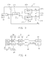
- FIG. 3 is a circuit diagram of the relay control device in accordance with the present invention.
- FIG. 4 is a circuit diagram of the module in accordance with the present invention.
- an optical return loss detecting device or exploring device for measuring the optical return loss (ORL) of a device under test (DUT) 32 .
- the detecting device comprises a light source 20 , an optical isolator 21 connected to the light source 20 for preventing reflected light by the DUT 32 entering the light source 20 , a first optical coupler 22 connected to the isolator 21 , a second optical coupler 24 connected to the first coupler 22 and the DUT 32 respectively, and a module 10 communicating with the second coupler 24 for performing test and calculation functions thereof.
- the light source 20 can be a laser diode.
- the first port 101 of the first coupler 22 is connected to the isolator 21 , the third port 103 is connected to the module 10 and the fourth port 104 thereof is connected to the first port 201 of the second coupler 24 .
- the second port 202 of the second coupler 24 is connected to the module 10 , the third port 203 is connected the DUT 32 , and the fourth port 204 can be made to consume possible light power propagated therethrough by means of directly coiled.
- the splitting ratio (coupling ratio) between the third port 103 and the fourth port 104 of the first coupler 22 can be 1:99, and no specific limitation is imposed upon the coupling ratio between the third port 203 and the fourth port 204 of the second coupler 24 , which can be 80:20 or 50:50.
- the module 10 includes an optical detecting device 12 which can be a photo diode (PD) device, an operation amplifying device (OP) 26 , an analog-digital conversion (AD) device 15 , a relay control device 27 , and a micro-control unit (MCU) 28 .
- the micro-control unit 28 can perform the function of 24 bit AD collection.
- the micro-control unit 28 is respectively connected to a liquid crystal device (LCD) 29 and a personal computer (PC) 30 via a RS-232 port.
- LCD liquid crystal device
- PC personal computer
- the relay control device 27 has first, second and third relay means 271 , 272 and 273 .
- the input port of the first relay 271 is connected to the output port of the operation amplifying device 26 .
- the input ports of the second and third relay 272 , 273 are respectively connected to the first and second output ports of the first relay means 271 .
- corresponding voltages are respectively applied to the first, second and third relay means 271 , 272 and 273 via according I/O ports.
- the relay control device 27 also comprises a capacitor 274 with one end thereof connected with the input port of the first relay means 271 , and first, second, third and fourth resistors 275 , 276 , 277 and 278 .
- One common end of the first, second, third and fourth resistors 275 , 276 , 277 and 278 are together connected to the end of the capacitor 274 opposite to the first relay means 271 .
- the other ends of the first and second resistors 275 , 276 which are respectively opposite to the capacitor 274 , are respectively connected to the first and second output ports of the second relay means 272 .
- the other ends of the third and fourth resistors 277 , 278 which are respectively opposite to the capacitor 274 , are respectively connected to the first and second output ports of the third relay means 273 .
- the output port of the operation amplifying device 26 is not only connected to the capacitor 274 , but also connected to the output port of the relay control device 27 and then send corresponding signals to the analog-digital conversion device 15 .
- the end of the capacitor 274 which is opposite to the first relay means 271 , is not only connected to the four resistors 275 , 276 , 277 and 278 , but also is respectively connected with the first input port of the operation amplifying device 26 and the output port of the optical exploring device 12 so as to function as a feedback circuit thereof.
- the second input port of the operation amplifying device 26 is grounded, and the voltage difference between the input port of the optical exploring device 12 and the second input port of the operation amplifying device 26 is pre-determined to be ⁇ 5v.
- FIG. 4 shows a detailed embodiment of the module 10 in accordance with the present invention.
- the optical exploring device 12 of the module 10 includes first and second optical detecting means 23 , 25 .
- the operation amplifying device 26 comprises first and second operation amplifiers 260 , 262 , among which the input port of the first optical detecting means 23 is connected to the third port 103 of the first coupler 22 , and the output port of the first optical detecting means 23 is connected to the input port of the first operation amplifier 260 .
- the input port of the second optical detecting means 25 is connected to the second port 202 of the second coupler 24 , and the output port thereof is connected to the input port of the second operation amplifier 262 .
- the module 10 further comprises an analog-digital conversion device 15 positioned between the operation amplifying device 26 and the micro-control unit 28 .
- the analog-digital conversion device 15 includes first and second analog-digital conversion means 150 and 152 , whose input ports thereof are both connected with the output ports of the first and second operation amplifiers 260 , 262 for converting corresponding analog signals into according digital signals which are to be sent to the micro-control unit 28 .
- the output port of the relay control device 27 is connected to the second analog-digital conversion means 152 .
- the light source 20 emits light to the isolator 21 thereby forming the light path ⁇ circle around ( 1 ) ⁇ .
- the light enters into the first coupler 22 after leaving the isolator 21 and then is divided into two portions which ext the first coupler 22 respectively via the third and fourth ports 103 and 104 thereby forming light paths ⁇ circle around ( 2 ) ⁇ and ⁇ circle around ( 3 ) ⁇ .
- the light path ⁇ circle around ( 2 ) ⁇ is directed to the first optical detecting means 23 and then is sent to the micro-control unit 28 via the operation amplifying device 26 .
- the light path ⁇ circle around ( 3 ) ⁇ is directed to the second coupler 24 and then further be divided into another two portions which are outputted of the second coupler 24 respectively via the third and fourth ports 203 and 204 thereby forming light paths ⁇ circle around ( 4 ) ⁇ and ⁇ circle around ( 5 ) ⁇ Among which, the light path ⁇ circle around ( 4 ) ⁇ is directed to the DUT 32 and the light path ⁇ circle around ( 5 ) ⁇ is coiled to be used up the light transmitted therethrough.
- a part of the reflected light by the DUT 32 via the light path ⁇ circle around ( 4 ) ⁇ is then reflected by the second coupler 24 to the isolator 21 so that no reflected light can be isolated before it can enter into the light source 20 .
- the other part of the reflected light by the DUT 32 will form the light path ⁇ circle around ( 4 ) ⁇ and then is inputted into the second optical detecting means 25 for converting corresponding optical signals into current signals which will be changed into voltage signals after passing through the second operation amplifier 262 and then are sent to the micro-control unit 28 by the relay control device 27 to be adjusted to a suitable level.
- the light inputted to the first optical detecting means 23 via the light path ⁇ circle around ( 2 ) ⁇ is changed into current signals which are then sent to the first operation amplifier 260 of the operation amplifying device 26 , where the current signals are changed into voltage signals and then are sent to the micro-control unit 28 .
- the values of the current outputted to the first analog-digital conversion device 152 can be adjusted at four different levels. This is achieved by controlling the second and third relay means 272 and 273 of the relay control device 27 so that correspondent first, second, third and fourth resistors 275 , 276 , 277 and 278 can be selected to be switched on thereby realizing the different current outputs to the first analog-digital conversion device 152 at different levels.
- the resistance values of the first, second, third and fourth resistors 275 , 276 , 277 and 278 can be 400 ohm, 20 K ohm, 1 M ohm and 50M ohm, which is increased by 50 multiples thereof., so as to control the second analog-digital conversion means 152 .
- the first analog-digital conversion means 150 is mainly used to monitor whether the power of the light source 20 varies or not, and then functions to adjust the detected signals.
- the voltage signals converted by the operation amplifying device 26 firstly go through the analog-digital conversion device 15 for converting corresponding analog signals into digital signals, and then are sent to the micro-control unit 28 .
- the micro-control unit 28 can finally get the value of the optical return loss by the DUT 32 by calculating the voltage or current values collected by the two AD collection paths of the first and second analog-digital conversion means 150 and 152 .
- the value of the optical return loss are then outputted to the LCD 29 to display thereon, and can send relevant information to the calculator 30 via RS232 port thereof.
- optical return loss measuring or exploring device 1 in accordance with the present invention can also have the function of measuring/exploring optical insertion loss thereof by simply modifying the exploring device 1 . For example, just remove the second coupler 24 and then connect the output port of the DUT 32 to the second optical detecting means 25 .
- the optical RL measuring or exploring device 1 can be modified to an optical time domain reflectometer (OTDR), which can measure the value of reflected light by a specific optical component or a specific interface which is positioned a certain distance away from the light source 20 thereof, thereby determining whether the optical component or interface is working normally or not.
- OTDR optical time domain reflectometer
- the optical RL measuring or exploring device 1 of the present invention When the optical RL measuring or exploring device 1 of the present invention is used to measure some faint reflected light, it adopts the solid-status relay control device 27 to replace a traditional analog switch, which can make the resistance thereof approaches zero when switched on thereby gaining a better linear performance thereof when optical signals are conversed into electrical signals so as to increase the exploring precision thereof.
- the coupling ratios of the first and second couplers 22 and 24 are respectively selected to be 99:1 and 80:20, which can ensure the high precision of the tested RL values thereof.
- the isolator 21 is added between the laser light source 20 and the first coupler 22 so that light reflected back from the light propagation paths thereof can be prevented enter the laser light source 20 , which ensures the stable output by the light source 20 .
- the optical RL measuring or exploring device 1 of the present invention is more compact in structure thereof, and interferences between the components therein can be effectively reduced consequently.
Landscapes
- Physics & Mathematics (AREA)
- Optics & Photonics (AREA)
- Chemical & Material Sciences (AREA)
- Analytical Chemistry (AREA)
- General Physics & Mathematics (AREA)
- Testing Of Optical Devices Or Fibers (AREA)
- Investigating Or Analysing Materials By Optical Means (AREA)
Applications Claiming Priority (2)
| Application Number | Priority Date | Filing Date | Title |
|---|---|---|---|
| TW093103827A TWI242942B (en) | 2004-02-17 | 2004-02-17 | Optical return loss detecting device |
| TW093103827 | 2004-02-17 |
Publications (2)
| Publication Number | Publication Date |
|---|---|
| US20050180747A1 US20050180747A1 (en) | 2005-08-18 |
| US7228024B2 true US7228024B2 (en) | 2007-06-05 |
Family
ID=34836997
Family Applications (1)
| Application Number | Title | Priority Date | Filing Date |
|---|---|---|---|
| US10/892,117 Expired - Fee Related US7228024B2 (en) | 2004-02-17 | 2004-07-16 | Optical return loss detecting device |
Country Status (2)
| Country | Link |
|---|---|
| US (1) | US7228024B2 (zh) |
| TW (1) | TWI242942B (zh) |
Cited By (4)
| Publication number | Priority date | Publication date | Assignee | Title |
|---|---|---|---|---|
| US20100117830A1 (en) * | 2006-12-29 | 2010-05-13 | Schlumberger Technology Corporation | Fault-tolerant distributed fiber optic intrusion detection |
| US8373785B2 (en) | 2004-08-11 | 2013-02-12 | Broadcom Corporation | Shallow trench isolation for active devices mounted on a CMOS substrate |
| US9222850B2 (en) | 2013-03-14 | 2015-12-29 | Axonoptics, Llc | Integrated optics reflectometer |
| US9557243B2 (en) | 2012-03-14 | 2017-01-31 | Axonoptics Llc | Integrated optics reflectometer |
Families Citing this family (11)
| Publication number | Priority date | Publication date | Assignee | Title |
|---|---|---|---|---|
| US7333043B2 (en) * | 2004-08-18 | 2008-02-19 | Broadcom Corporation | Active pixel array with matching analog-to-digital converters for image processing |
| US7145188B2 (en) * | 2004-08-19 | 2006-12-05 | Broadcom Corporation | Apparatus and method of image processing to avoid image saturation |
| US7236682B2 (en) * | 2004-10-01 | 2007-06-26 | Finisar Corporation | Optical return loss measurement |
| CN103297125B (zh) * | 2013-03-21 | 2016-03-30 | 镇江奥菲特光电科技有限公司 | 光纤分路器自动测试系统 |
| US20160197672A1 (en) * | 2013-07-22 | 2016-07-07 | Afl Telecommunications Llc | Method of measuring optical return loss |
| CN103647600B (zh) * | 2013-12-24 | 2015-12-30 | 武汉光迅科技股份有限公司 | 一种多通道智能光学测试装置 |
| CN109157754B (zh) * | 2017-10-30 | 2020-11-03 | 武汉奇致激光技术股份有限公司 | 一种用于双波长激光治疗机切换控制系统及其控制方法 |
| CN110518971B (zh) * | 2019-09-27 | 2024-05-31 | 中国电子科技集团公司第三十四研究所 | 一种基于水下采样的有中继海底光缆扰动监测系统 |
| CN112082734B (zh) * | 2020-09-04 | 2022-06-21 | 哈尔滨工程大学 | 一种用于y波导反射特性测试的标定方法 |
| CN112729774B (zh) * | 2020-12-03 | 2022-06-28 | 四川知周科技有限责任公司 | 共光路激光点火及通路损耗检测装置 |
| CN118393330A (zh) * | 2024-06-21 | 2024-07-26 | 四川泰瑞创通讯技术股份有限公司 | 回损测试电路及其控制方法、系统以及存储介质 |
Citations (8)
| Publication number | Priority date | Publication date | Assignee | Title |
|---|---|---|---|---|
| US5221839A (en) | 1991-02-15 | 1993-06-22 | Hewlett-Packard Company | Double bevel gradient-index rod lens optical receiver having high optical return loss |
| US5822094A (en) | 1996-01-18 | 1998-10-13 | Northern Telecom Limited | Self-stimulation signal detection in an optical transmission system |
| US6111676A (en) | 1998-02-26 | 2000-08-29 | Nortel Networks Corporation | Wavelength specific optical reflection meter/locator in signatured wavelength division multiplexed systems |
| CN2540067Y (zh) | 2002-04-30 | 2003-03-12 | 武汉邮电科学研究院 | 光通信用在线监视装置 |
| CN1420374A (zh) | 2002-12-23 | 2003-05-28 | 浙江大学 | 低回损蚀刻衍射光栅波分复用器 |
| US6580498B1 (en) * | 2001-02-02 | 2003-06-17 | Nortel Networks Limited | Optical return loss detector for optical transmission systems |
| US6810210B1 (en) * | 2000-07-31 | 2004-10-26 | Nortel Networks Limited | Communication path impairment detection for duplex optic communication link |
| US7016024B2 (en) * | 2004-05-18 | 2006-03-21 | Net Test (New York) Inc. | Accuracy automated optical time domain reflectometry optical return loss measurements using a “Smart” Test Fiber Module |
-
2004
- 2004-02-17 TW TW093103827A patent/TWI242942B/zh not_active IP Right Cessation
- 2004-07-16 US US10/892,117 patent/US7228024B2/en not_active Expired - Fee Related
Patent Citations (8)
| Publication number | Priority date | Publication date | Assignee | Title |
|---|---|---|---|---|
| US5221839A (en) | 1991-02-15 | 1993-06-22 | Hewlett-Packard Company | Double bevel gradient-index rod lens optical receiver having high optical return loss |
| US5822094A (en) | 1996-01-18 | 1998-10-13 | Northern Telecom Limited | Self-stimulation signal detection in an optical transmission system |
| US6111676A (en) | 1998-02-26 | 2000-08-29 | Nortel Networks Corporation | Wavelength specific optical reflection meter/locator in signatured wavelength division multiplexed systems |
| US6810210B1 (en) * | 2000-07-31 | 2004-10-26 | Nortel Networks Limited | Communication path impairment detection for duplex optic communication link |
| US6580498B1 (en) * | 2001-02-02 | 2003-06-17 | Nortel Networks Limited | Optical return loss detector for optical transmission systems |
| CN2540067Y (zh) | 2002-04-30 | 2003-03-12 | 武汉邮电科学研究院 | 光通信用在线监视装置 |
| CN1420374A (zh) | 2002-12-23 | 2003-05-28 | 浙江大学 | 低回损蚀刻衍射光栅波分复用器 |
| US7016024B2 (en) * | 2004-05-18 | 2006-03-21 | Net Test (New York) Inc. | Accuracy automated optical time domain reflectometry optical return loss measurements using a “Smart” Test Fiber Module |
Cited By (5)
| Publication number | Priority date | Publication date | Assignee | Title |
|---|---|---|---|---|
| US8373785B2 (en) | 2004-08-11 | 2013-02-12 | Broadcom Corporation | Shallow trench isolation for active devices mounted on a CMOS substrate |
| US20100117830A1 (en) * | 2006-12-29 | 2010-05-13 | Schlumberger Technology Corporation | Fault-tolerant distributed fiber optic intrusion detection |
| US8947232B2 (en) * | 2006-12-29 | 2015-02-03 | Schlumberger Technology Corporation | Fault-tolerant distributed fiber optic intrusion detection |
| US9557243B2 (en) | 2012-03-14 | 2017-01-31 | Axonoptics Llc | Integrated optics reflectometer |
| US9222850B2 (en) | 2013-03-14 | 2015-12-29 | Axonoptics, Llc | Integrated optics reflectometer |
Also Published As
| Publication number | Publication date |
|---|---|
| TWI242942B (en) | 2005-11-01 |
| US20050180747A1 (en) | 2005-08-18 |
| TW200529587A (en) | 2005-09-01 |
Similar Documents
| Publication | Publication Date | Title |
|---|---|---|
| US7228024B2 (en) | Optical return loss detecting device | |
| US8213002B2 (en) | PON tester | |
| CN100541158C (zh) | 光纤偏振波模式分散的测定方法及其测定装置 | |
| EP0926479B1 (en) | Optical loss measurement | |
| EP0418509A2 (en) | Calibration of a lightwave component analyzer for testing optical devices | |
| CN111678584A (zh) | 一种带光源频移校准辅助通道的光纤振动测量装置及方法 | |
| US7920253B2 (en) | Polarization optical time domain reflectometer and method of determining PMD | |
| CN111412947A (zh) | 一种全分布式opgw光缆覆冰在线监测装置及控制方法 | |
| Laferriere et al. | Reference guide to fiber optic testing | |
| CN108801305B (zh) | 基于阶梯脉冲自放大的布里渊光时域反射仪的方法及装置 | |
| CN212030564U (zh) | 一种光源频移校准辅助通道结构及光纤振动测量装置 | |
| US6317214B1 (en) | Method and apparatus to determine a measurement of optical multiple path interference | |
| CN218865126U (zh) | 一种基于otdr的融合系统 | |
| CN110178320A (zh) | 具有标准化输出的高分辨率线路监测技术和使用该技术的光通信系统 | |
| CN201885732U (zh) | 一种融合光纤布里渊频移器的分布式光纤布里渊传感器 | |
| CN111122005B (zh) | 一种融合光纤光栅传感器的光纤监测装置 | |
| CN113483914A (zh) | 基于少模光纤的混沌bocda温度应变测量装置 | |
| CA2219286A1 (en) | Measurement of polarization mode dispersion | |
| CN114414528A (zh) | 基于5g微波光子信号的双光纤端面干涉盐度检测方法 | |
| CN113252089A (zh) | 一种分布式光纤传感装置 | |
| CN110071759B (zh) | 一种基于偏振白光干涉的光缆故障定位装置及方法 | |
| CN110375960B (zh) | 一种基于超连续谱光源otdr的装置及方法 | |
| CN111162835A (zh) | 光时域反射仪 | |
| CN112104415A (zh) | 一种采用edfa放大装置检测瑞利散射信号强度的系统 | |
| CN216524011U (zh) | 一种长距离布里渊光时域反射仪监测装置 |
Legal Events
| Date | Code | Title | Description |
|---|---|---|---|
| AS | Assignment |
Owner name: ASIA OPTICAL CO., INC., TAIWAN Free format text: ASSIGNMENT OF ASSIGNORS INTEREST;ASSIGNOR:WANG, XIAO-YONG;REEL/FRAME:015584/0926 Effective date: 20040116 |
|
| FPAY | Fee payment |
Year of fee payment: 4 |
|
| REMI | Maintenance fee reminder mailed | ||
| LAPS | Lapse for failure to pay maintenance fees | ||
| STCH | Information on status: patent discontinuation |
Free format text: PATENT EXPIRED DUE TO NONPAYMENT OF MAINTENANCE FEES UNDER 37 CFR 1.362 |
|
| STCH | Information on status: patent discontinuation |
Free format text: PATENT EXPIRED DUE TO NONPAYMENT OF MAINTENANCE FEES UNDER 37 CFR 1.362 |
|
| FP | Lapsed due to failure to pay maintenance fee |
Effective date: 20150605 |