US7221019B2 - Short-channel Schottky-barrier MOSFET device and manufacturing method - Google Patents
Short-channel Schottky-barrier MOSFET device and manufacturing method Download PDFInfo
- Publication number
- US7221019B2 US7221019B2 US11/478,478 US47847806A US7221019B2 US 7221019 B2 US7221019 B2 US 7221019B2 US 47847806 A US47847806 A US 47847806A US 7221019 B2 US7221019 B2 US 7221019B2
- Authority
- US
- United States
- Prior art keywords
- channel
- drain
- source
- present
- mosfet
- Prior art date
- Legal status (The legal status is an assumption and is not a legal conclusion. Google has not performed a legal analysis and makes no representation as to the accuracy of the status listed.)
- Expired - Fee Related
Links
Images


Classifications
-
- H—ELECTRICITY
- H10—SEMICONDUCTOR DEVICES; ELECTRIC SOLID-STATE DEVICES NOT OTHERWISE PROVIDED FOR
- H10P—GENERIC PROCESSES OR APPARATUS FOR THE MANUFACTURE OR TREATMENT OF DEVICES COVERED BY CLASS H10
- H10P30/00—Ion implantation into wafers, substrates or parts of devices
- H10P30/20—Ion implantation into wafers, substrates or parts of devices into semiconductor materials, e.g. for doping
- H10P30/202—Ion implantation into wafers, substrates or parts of devices into semiconductor materials, e.g. for doping characterised by the semiconductor materials
- H10P30/204—Ion implantation into wafers, substrates or parts of devices into semiconductor materials, e.g. for doping characterised by the semiconductor materials into Group IV semiconductors
-
- H—ELECTRICITY
- H10—SEMICONDUCTOR DEVICES; ELECTRIC SOLID-STATE DEVICES NOT OTHERWISE PROVIDED FOR
- H10D—INORGANIC ELECTRIC SEMICONDUCTOR DEVICES
- H10D30/00—Field-effect transistors [FET]
- H10D30/01—Manufacture or treatment
- H10D30/021—Manufacture or treatment of FETs having insulated gates [IGFET]
- H10D30/027—Manufacture or treatment of FETs having insulated gates [IGFET] of lateral single-gate IGFETs
- H10D30/0277—Manufacture or treatment of FETs having insulated gates [IGFET] of lateral single-gate IGFETs forming conductor-insulator-semiconductor or Schottky barrier source or drain regions
-
- H—ELECTRICITY
- H10—SEMICONDUCTOR DEVICES; ELECTRIC SOLID-STATE DEVICES NOT OTHERWISE PROVIDED FOR
- H10D—INORGANIC ELECTRIC SEMICONDUCTOR DEVICES
- H10D62/00—Semiconductor bodies, or regions thereof, of devices having potential barriers
- H10D62/10—Shapes, relative sizes or dispositions of the regions of the semiconductor bodies; Shapes of the semiconductor bodies
- H10D62/17—Semiconductor regions connected to electrodes not carrying current to be rectified, amplified or switched, e.g. channel regions
- H10D62/213—Channel regions of field-effect devices
- H10D62/221—Channel regions of field-effect devices of FETs
- H10D62/235—Channel regions of field-effect devices of FETs of IGFETs
- H10D62/314—Channel regions of field-effect devices of FETs of IGFETs having vertical doping variations
-
- H—ELECTRICITY
- H10—SEMICONDUCTOR DEVICES; ELECTRIC SOLID-STATE DEVICES NOT OTHERWISE PROVIDED FOR
- H10D—INORGANIC ELECTRIC SEMICONDUCTOR DEVICES
- H10D64/00—Electrodes of devices having potential barriers
- H10D64/60—Electrodes characterised by their materials
- H10D64/64—Electrodes comprising a Schottky barrier to a semiconductor
- H10D64/647—Schottky drain or source electrodes for IGFETs
-
- H—ELECTRICITY
- H10—SEMICONDUCTOR DEVICES; ELECTRIC SOLID-STATE DEVICES NOT OTHERWISE PROVIDED FOR
- H10D—INORGANIC ELECTRIC SEMICONDUCTOR DEVICES
- H10D84/00—Integrated devices formed in or on semiconductor substrates that comprise only semiconducting layers, e.g. on Si wafers or on GaAs-on-Si wafers
- H10D84/01—Manufacture or treatment
- H10D84/0123—Integrating together multiple components covered by H10D12/00 or H10D30/00, e.g. integrating multiple IGBTs
- H10D84/0126—Integrating together multiple components covered by H10D12/00 or H10D30/00, e.g. integrating multiple IGBTs the components including insulated gates, e.g. IGFETs
- H10D84/0165—Integrating together multiple components covered by H10D12/00 or H10D30/00, e.g. integrating multiple IGBTs the components including insulated gates, e.g. IGFETs the components including complementary IGFETs, e.g. CMOS devices
- H10D84/017—Manufacturing their source or drain regions, e.g. silicided source or drain regions
-
- H—ELECTRICITY
- H10—SEMICONDUCTOR DEVICES; ELECTRIC SOLID-STATE DEVICES NOT OTHERWISE PROVIDED FOR
- H10D—INORGANIC ELECTRIC SEMICONDUCTOR DEVICES
- H10D84/00—Integrated devices formed in or on semiconductor substrates that comprise only semiconducting layers, e.g. on Si wafers or on GaAs-on-Si wafers
- H10D84/01—Manufacture or treatment
- H10D84/0123—Integrating together multiple components covered by H10D12/00 or H10D30/00, e.g. integrating multiple IGBTs
- H10D84/0126—Integrating together multiple components covered by H10D12/00 or H10D30/00, e.g. integrating multiple IGBTs the components including insulated gates, e.g. IGFETs
- H10D84/0165—Integrating together multiple components covered by H10D12/00 or H10D30/00, e.g. integrating multiple IGBTs the components including insulated gates, e.g. IGFETs the components including complementary IGFETs, e.g. CMOS devices
- H10D84/0172—Manufacturing their gate conductors
- H10D84/0174—Manufacturing their gate conductors the gate conductors being silicided
-
- H—ELECTRICITY
- H10—SEMICONDUCTOR DEVICES; ELECTRIC SOLID-STATE DEVICES NOT OTHERWISE PROVIDED FOR
- H10D—INORGANIC ELECTRIC SEMICONDUCTOR DEVICES
- H10D84/00—Integrated devices formed in or on semiconductor substrates that comprise only semiconducting layers, e.g. on Si wafers or on GaAs-on-Si wafers
- H10D84/01—Manufacture or treatment
- H10D84/0123—Integrating together multiple components covered by H10D12/00 or H10D30/00, e.g. integrating multiple IGBTs
- H10D84/0126—Integrating together multiple components covered by H10D12/00 or H10D30/00, e.g. integrating multiple IGBTs the components including insulated gates, e.g. IGFETs
- H10D84/0165—Integrating together multiple components covered by H10D12/00 or H10D30/00, e.g. integrating multiple IGBTs the components including insulated gates, e.g. IGFETs the components including complementary IGFETs, e.g. CMOS devices
- H10D84/0172—Manufacturing their gate conductors
- H10D84/0177—Manufacturing their gate conductors the gate conductors having different materials or different implants
-
- H—ELECTRICITY
- H10—SEMICONDUCTOR DEVICES; ELECTRIC SOLID-STATE DEVICES NOT OTHERWISE PROVIDED FOR
- H10D—INORGANIC ELECTRIC SEMICONDUCTOR DEVICES
- H10D84/00—Integrated devices formed in or on semiconductor substrates that comprise only semiconducting layers, e.g. on Si wafers or on GaAs-on-Si wafers
- H10D84/01—Manufacture or treatment
- H10D84/02—Manufacture or treatment characterised by using material-based technologies
- H10D84/03—Manufacture or treatment characterised by using material-based technologies using Group IV technology, e.g. silicon technology or silicon-carbide [SiC] technology
- H10D84/038—Manufacture or treatment characterised by using material-based technologies using Group IV technology, e.g. silicon technology or silicon-carbide [SiC] technology using silicon technology, e.g. SiGe
-
- H—ELECTRICITY
- H10—SEMICONDUCTOR DEVICES; ELECTRIC SOLID-STATE DEVICES NOT OTHERWISE PROVIDED FOR
- H10D—INORGANIC ELECTRIC SEMICONDUCTOR DEVICES
- H10D84/00—Integrated devices formed in or on semiconductor substrates that comprise only semiconducting layers, e.g. on Si wafers or on GaAs-on-Si wafers
- H10D84/80—Integrated devices formed in or on semiconductor substrates that comprise only semiconducting layers, e.g. on Si wafers or on GaAs-on-Si wafers characterised by the integration of at least one component covered by groups H10D12/00 or H10D30/00, e.g. integration of IGFETs
- H10D84/86—Integrated devices formed in or on semiconductor substrates that comprise only semiconducting layers, e.g. on Si wafers or on GaAs-on-Si wafers characterised by the integration of at least one component covered by groups H10D12/00 or H10D30/00, e.g. integration of IGFETs of Schottky-barrier gate FETs
-
- H—ELECTRICITY
- H10—SEMICONDUCTOR DEVICES; ELECTRIC SOLID-STATE DEVICES NOT OTHERWISE PROVIDED FOR
- H10P—GENERIC PROCESSES OR APPARATUS FOR THE MANUFACTURE OR TREATMENT OF DEVICES COVERED BY CLASS H10
- H10P30/00—Ion implantation into wafers, substrates or parts of devices
- H10P30/20—Ion implantation into wafers, substrates or parts of devices into semiconductor materials, e.g. for doping
- H10P30/21—Ion implantation into wafers, substrates or parts of devices into semiconductor materials, e.g. for doping of electrically active species
- H10P30/212—Through-implantation
-
- H—ELECTRICITY
- H10—SEMICONDUCTOR DEVICES; ELECTRIC SOLID-STATE DEVICES NOT OTHERWISE PROVIDED FOR
- H10P—GENERIC PROCESSES OR APPARATUS FOR THE MANUFACTURE OR TREATMENT OF DEVICES COVERED BY CLASS H10
- H10P30/00—Ion implantation into wafers, substrates or parts of devices
- H10P30/20—Ion implantation into wafers, substrates or parts of devices into semiconductor materials, e.g. for doping
- H10P30/28—Ion implantation into wafers, substrates or parts of devices into semiconductor materials, e.g. for doping characterised by an annealing step, e.g. for activation of dopants
-
- H—ELECTRICITY
- H10—SEMICONDUCTOR DEVICES; ELECTRIC SOLID-STATE DEVICES NOT OTHERWISE PROVIDED FOR
- H10D—INORGANIC ELECTRIC SEMICONDUCTOR DEVICES
- H10D30/00—Field-effect transistors [FET]
- H10D30/01—Manufacture or treatment
- H10D30/021—Manufacture or treatment of FETs having insulated gates [IGFET]
- H10D30/0212—Manufacture or treatment of FETs having insulated gates [IGFET] using self-aligned silicidation
Definitions
- the present invention relates generally to the field of metal oxide semiconductor field effect transistors (MOSFETs), and has specific application to the fabrication of these devices in the context of an integrated circuit (IC).
- MOSFETs metal oxide semiconductor field effect transistors
- MOSFETs Metal-Oxide-Semiconductor-Field-Effect-Transistors
- L the distance that charge carriers must travel to pass through the device, and a reduction in this length simultaneously implies higher current drives, reduced parasitic resistances and capacitances and improved high-frequency performance.
- a common figure-of-merit is the power-delay product, and this generalized measure of transistor performance improves as the cube of the inverse of the channel length (1/L 3 ). This explains the tremendous incentive that IC manufacturers have to reduce the channel length as much as manufacturing capabilities will allow.
- MOS transistors behave like switches. When “on,” they drive relatively large amounts of current, and when turned “off” they are characterized by a certain amount of leakage current. As channel lengths are reduced, drive currents increase, which is beneficial for circuit performance as stated above. However, leakage currents increase as well. Leaky transistors contribute to quiescent power dissipation (the power dissipated by an IC when idle) and in extreme cases can affect the transfer of binary information during active operation. Device designers therefore have good reason to keep leakage currents low as channel lengths are reduced.
- MOS transistor leakage currents are traditionally controlled by introducing controlled amounts of impurities (dopants) into the channel region of the device, and by tailoring the source/drain lateral and vertical doping distributions.
- dopants impurities
- these approaches are effective in shoring up the potential barrier internal to the MOS transistor and therefore reducing the leakage current, they can also contribute to degraded drive current and increased parasitic capacitance—the very items that channel length reduction is meant to improve.
- the channel and tailored source/drain dopants are introduced, the manufacturing cost can be affected significantly. Given traditional MOS transistor design and architecture, there are only limited solutions to the trade-off between drive current, leakage current, parasitic capacitance and resistance, and manufacturing complexity/cost.
- the present invention offers a new relationship between these competing requirements, and makes possible MOS devices with characteristics that are not achievable with traditional (impurity doped) MOS architectures.
- the use of metal for the source and drain and a simple, uniformly implanted channel dopant profile provides for improvements to device characteristics in terms of reduced parasitic capacitance, reduced statistical variations in these characteristics (especially as the channel length is decreased) and reduced manufacturing cost and complexity.
- FIG. 1 illustrates an exemplary long-channel conventional MOS device ( 100 ) that comprises an impurity doped source ( 101 ), an impurity doped drain ( 102 ), a conventional MOS type gate stack ( 103 ), and a laterally uniform channel doping profile ( 104 ) in the substrate to assist in the control of source-to-drain leakage currents.
- Devices are electrically isolated from each other via a field oxide ( 105 ).
- Such channel dopant profiles are common in devices with channel lengths down to approximately 200 nanometers (nm).
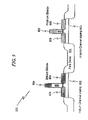
- the exemplary short-channel MOS device ( 200 ) has some elements similar to the long-channel MOS device ( 100 ).
- the structure comprises a conventional impurity doped source ( 201 ) and drain ( 202 ) as well as a conventional MOS gate stack ( 203 ) (width ⁇ ⁇ 100 nm, corresponding to the channel length L).
- the structure further comprises shallow, impurity doped extensions for the source ( 208 ) and drain ( 209 ) electrodes which are used in conjunction with drain ( 206 ) and source ( 207 ) pocket doping as well as conventional channel doping ( 204 ) to control source to drain leakage currents.
- Source and drain electrodes ( 201 ) and ( 202 ) and their respective extensions ( 208 ) and ( 209 ) are all of the same doping polarity (either N-type or P-type) and are of the opposite polarity from the channel ( 204 ) and pocket doping elements ( 206 ) and ( 207 ).
- a field oxide ( 205 ) electrically isolates devices from each other.
- Halo/Pocket implants along with shallow source/drain extensions add complexity to the manufacturing process. At least two additional lithography steps, as well as the associated cleans, implants, metrology, etc. are required to implement these process steps. As lithography is one of the most (if not the most) expensive process modules in the production process, this is a significant increase in manufacturing cost. Halo and Pocket implants as well as shallow source/drain extensions can also add parasitic capacitance and a random statistical variation to device electrical characteristics.
- Q. T. Zhao is the next author to explicitly address the issue of channel doping to control leakage currents. His approach (uniform doping of the substrate to quite high levels (10 17 /cm 3 )) is well known to be non-optimal for short channel devices. Although he is successful in reducing leakage currents, he does so at the expense of increased source/drain-to-substrate capacitance. See Q. T. Zhao, F. Klinkhammer, M. Dolle, L. Kappius, S.
- W. Saitoh reports on a device built on SOI substrates but does not discuss substrate doping in this context. See W. Saitoh, S. Yamagami, A. Itoh, M. Asada, “35 nm metal gate SOI-P-MOSFETs with PtSi Schottky source/drain,” Device Research Conference, Jun. 28–30, 1999, Santa Barbara, Calif., Paper II.A.6, page 30.
- C. Wang mentions the use of “a layer of fully-depleted dopants beneath the active region” and “preimplanting a thin subsurface layer of fully depleted dopants” to control leakage currents, but does not describe the lateral uniformity or lack thereof of the doping profile, or how one might go about producing the “layer”. See C. Wang, John P. Snyder, J. R. Tucker, “Sub-40 nm PtSi Schottky source/drain metal-oxide-semiconductor field-effect-transistors,” APPLIED PHYSICS LETTERS, Vol. 74 No. 8, 22 Feb. 1999, pages 1174; C. Wang, John P. Snyder, J. R. Tucker, “Sub-50 nm PtSi Schottky source/drain P-MOSFETs,” Annual Device Research Conference Digest 1998, pages 72–73.
- the proposed invention offers a novel and non-obvious MOSFET device and fabrication approach with many advantages over the current state-of-the-art.
- the objects of the present invention are (among others) to circumvent the deficiencies in the prior art and affect one or more of the following objectives:
- an exemplary embodiment of the present invention ( 300 ) consists simply of a conventional MOS gate stack ( 303 ) (gate electrode on silicon dioxide on a silicon substrate), metal source ( 301 ) and/or drain ( 302 ) electrodes, and channel dopants ( 304 ) that vary significantly in the vertical direction but not in the lateral direction.
- a field oxide ( 305 ) electrically isolates devices from each other.
- the Schottky (or Schottky-like) barriers ( 307 , 308 ) that exist along the interface of the corresponding metal source/drain ( 301 , 302 ) and the silicon substrate ( 306 ) act as an inherent pocket or halo implant and does so without added parasitic capacitance. It also eliminates the need for shallow source/drain extensions as the metal source/drain is by its nature shallow and highly conductive. Significant reductions in manufacturing complexity are therefore achieved by simultaneous elimination of the halo/pocket implants and the source/drain extensions. These are also major advantages over conventionally-architected-channel MOS devices.
- the metal source/drain (which replaces the conventional impurity doped source/drain) has a natural, very consistent and atomically abrupt Schottky barrier ( 307 , 308 ) with the silicon substrate ( 306 ) whose position and magnitude are independent of channel length, and because this barrier essentially plays the role of the halo/pocket implant (making these implants unnecessary), statistical variations due to random placement of atoms during the source/drain and halo/pocket implants are essentially eliminated. This fact remains true and even becomes more true as the channel length is reduced.
- the metal source/drain MOS architecture Another benefit of the metal source/drain MOS architecture is the unconditional elimination of the parasitic bipolar gain.
- the parasitic bipolar gain is a direct result of using opposite doping types for the source/drain and substrate regions, and can result in latch-up and other deleterious effects.
- the source/drain electrodes are constructed of metal, this parasitic gain is eliminated. This makes the metal source/drain architecture ideal for (among other things) high-radiation environments.
- FIG. 1 illustrates a prior art long channel, impurity doped source/drain device
- FIG. 2 illustrates a prior art short channel, impurity doped source/drain device with pocket implants and source/drain extensions
- FIG. 3 illustrates an exemplary embodiment of the present invention as applied to a short channel, metal source/drain device without pocket implants
- FIG. 4 illustrates an exemplary embodiment of the present invention process fabrication step using an implanted silicon substrate with approximately 200 A screen oxide
- FIG. 5 illustrates an exemplary embodiment of the present invention process fabrication step using a patterned in-situ doped silicon film on thin gate oxide
- FIG. 6 illustrates an exemplary embodiment of the present invention process fabrication step using a formation of thin oxide sidewalls, and exposure of silicon in the gate, source and drain areas;
- FIG. 7 illustrates an exemplary embodiment of the present invention process fabrication step using a metal deposition and solicidation anneal.
- FIG. 8 illustrates an exemplary embodiment of the present invention process fabrication step using a removal of unreacted metal from the sidewalls
- FIG. 9 illustrates an exemplary embodiment of the present invention process fabrication resulting structure.
- In-situ phosphorous doped silicon, Erbium silicide and Indium channel implants are used for the N-type device for the gate electrode, source/drain electrodes and channel doping respectively.
- the P-type devices make use of in-situ Boron doped silicon, Platinum Silicide and Arsenic channel implants.
- the channel dopant concentrations vary significantly in the vertical direction but not in the lateral direction. Gate lengths are typically ⁇ 100 nm, but may be longer;
- FIG. 10 illustrates an exemplary general system process flowchart showing a method of producing superior MOSFET devices
- FIG. 11 illustrates an exemplary detailed system process flowchart showing a method of producing superior MOSFET devices.
- the present invention may be aptly described in terms of exemplary system block diagrams and procedural flowcharts. While these items are sufficient to instruct one of ordinary skill in the art the teachings of the present invention, they should not be strictly construed as limiting the scope of the present invention.
- system block diagrams may be combined and rearranged with no loss of generality, and procedural steps may be added or subtracted, and rearranged in order to achieve the same effect with no loss of teaching generality.
- the present invention as depicted in the attached exemplary system block diagrams and procedural flowcharts is for teaching purposes only and may be reworked by one skilled in the art depending on the intended target application.
- predetermined region will be defined to encompass the area centered at the heart of the active device (MOSFET).
- MOSFET active device
- all the process steps mentioned in the context of a MOSFET will create a gate, source/drain, and/or channel doping profiles as well as other structures in an area proximal to the predetermined regions or heart of the active device.
- the present invention places no restrictions on what occurs outside this context, far from the heart of the active device.
- predetermined region will generally be spoken of in terms of a MOSFET device, this in no way limits the scope of the present invention.
- any device capable of regulating the flow of electrical current may be considered to have a predetermined region in proximity to its active current carrying region.
- the present invention is particularly suitable for use with MOSFET semiconductor devices, but the use of the present teachings is not limited to this particular application.
- Other semiconductor devices, whether integrated or not, may be applied to the present invention teachings.
- this specification speaks in terms of ‘MOSFET’ devices, this term should be interpreted broadly to include any device for regulating the flow of electrical current having a conducting channel that has two or more points of electrical contact.
- the present invention is particularly suitable for use in situations where short channel length MOSFETs are to be fabricated, especially in the range of channel lengths ⁇ 100 nm.
- nothing in the teachings of the present invention limits application of the teachings of the present invention to these short channel length devices.
- Advantageous use of the teachings of the present invention may be had with channel lengths of any dimension.
- impurity atoms are selected from the group consisting of Arsenic, Phosphorous, Antimony, Boron, Indium, and/or Gallium as being within the scope of the teachings of the present invention.
- source and drain should be interpreted to include the variants ‘drain’ and ‘source’ as well as ‘source or drain’ and ‘source and drain’.
- the present invention specifically anticipates that in some circumstances an interfacial layer may be utilized between the silicon substrate and the actual Schottky barrier metal.
- the present invention specifically anticipates ‘Schottky-like’ junctions and their equivalents to be useful in implementing the present invention.
- the interfacial layer may comprise materials that have conductive, semi-conductive, and/or insulator-like properties.
- FIGS. 4–9 One possible process flow for the fabrication of channel implanted, short channel ( ⁇ 100 nm) metal source/drain MOS devices ( 400 ) is illustrated in FIGS. 4–9 . While this exemplary process flow is just exemplary of the broad teachings of the present invention, it will prove very instructive to one skilled in the art to teach the fundamental concepts of the present invention. This exemplary process flow may be described as follows:
- a thin screen oxide ( 401 ) is grown (approximately 200 ⁇ ) to act as an implant mask.
- the appropriate channel dopant species ( 403 ) for example Arsenic and Indium for P-type and N-type devices respectively
- the channel doping profile has a peak concentration of approximately 2 ⁇ 10 18 cm ⁇ 3 located at a depth of approximately 50 nm in the channel region.
- the dopant concentration at the gate insulator interface to the channel region is 4 ⁇ 10 16 cm ⁇ 3 .
- the channel implant may have a peak dopant concentration of approximately 10 18 cm ⁇ 3 to 10 19 cm ⁇ 3 located at a depth of approximately 25–100 nm below the gate insulator.
- the Schottky barrier MOS device dopant concentration is 10 16 to 10 17 cm ⁇ 3 or approximately 90–99% lower compared to a conventional doped source/drain device. Reduced channel doping provides improved effective carrier mobility and reduced junction and gate capacitance.
- the screen oxide is then removed in hydro-fluoric acid, and a thin gate oxide ( 501 ) (approximately 35 ⁇ ) is grown.
- the gate oxide growth is immediately followed by an in-situ doped silicon film.
- the film is heavily doped with, for example, Phosphorous for an N-type device and Boron for a P-type device.
- the gate electrode ( 502 ) is patterned as shown in the process step ( 500 ) illustrated in FIG. 5 .
- a thin oxide (approximately 100 ⁇ ) is then thermally grown on the top surface and sidewalls of the silicon gate electrode.
- an anisotropic etch is then used to remove the oxide layers on the horizontal surfaces (and thus expose the silicon ( 601 )), while preserving them on the vertical surfaces.
- a sidewall oxide ( 602 ) is formed, and the dopants both in the gate electrode and in the channel region of the device are electrically activated as shown in the process step ( 600 ) illustrated in FIG. 6 .
- the final step encompasses depositing an appropriate metal (for example, Platinum for the P-type device and Erbium for the N-type device) as a blanket film (approximately 400 ⁇ ) on all exposed surfaces.
- an appropriate metal for example, Platinum for the P-type device and Erbium for the N-type device
- the wafer is then annealed for a specified time at a specified temperature (for example, 400° C. for 45 minutes) so that, at all places where the metal is in direct contact with the silicon, a chemical reaction takes place that converts the metal to a metal silicide ( 701 ).
- the metal that was in direct contact with a non-silicon surface ( 702 ) is left unaffected as shown in the process step ( 700 ) illustrated in FIG. 7 .
- a wet chemical etch (aqua regia for Platinum, HNO 3 for Erbium) is then used to remove the unreacted metal while leaving the metal-silicide untouched.
- the channel implanted, short channel Schottky barrier MOS device is now complete and ready for electrical contacting to gate, source, and drain as shown in the process step ( 800 ) illustrated in FIG. 8 .
- FIG. 9 shows a preferred exemplary embodiment of the invention, as exemplified by two final complementary MOSFET structures ( 900 ).
- This embodiment consists of N-channel devices fabricated with Erbium Silicide ( 904 ) for the source/drain regions, and a P-channel device fabricated with Platinum Silicide ( 905 ).
- Channel dopants Vertically varying, laterally non-varying Indium ( 902 ) and Arsenic ( 903 ) layers are used as the channel dopants for the N-channel and P-channel devices respectively. These dopant atoms are used due to their relatively low rates of diffusion through the silicon lattice (compared to Phosphorous and Boron, the other two possible candidates for channel dopants). This allows for greater thermal budget during fabrication of the device, and therefore less statistical variation in the characteristics of the finished product.
- the gate electrodes are fabricated from in-situ Phosphorous and Boron doped polysilicon films for the N-type ( 906 ) and P-type ( 907 ) devices respectively.
- Phosphorous and Boron are used due to their large solid-solubilities (compared to Arsenic and Indium).
- the electrodes are doped via the use of an in-situ method, wherein the impurity atoms are deposited at the same time the silicon atoms are. Such a method can achieve very large dopant concentrations (approximately 10 21 /cm3) and a uniform distribution throughout the thickness of the film.
- Another option for doping the silicon gate is ion-implantation. This method suffers from several practical problems including charging damage to the thin gate oxide, and the need to redistribute the highly non-uniform as-implanted gate dopants to achieve high doping levels at the gate oxide interface.
- the gate electrodes ( 906 ) and ( 907 ) are less than 100 nm in width (corresponding to the channel length L), as it is in this regime that the advantages of the Schottky barrier architecture over the conventional architecture become apparent. These include simplified processing due to the absence of need for pocket implants, and the resulting reduction in yield loss, capacitance and statistical variations in finished products.
- Devices are separated from each other by a thermally grown oxide (called a Field Oxide) ( 901 ) that works in conjunction with the channel dopants to electrically isolate the devices from each other.
- a Field Oxide a thermally grown oxide
- an exemplary generalized MOSFET device process fabrication flow starts with a semiconductor substrate having means for electrically isolating transistors ( 1000 ). On this substrate, channel dopants are introduced in such a way that the dopant concentration varies significantly in the vertical but not the lateral direction ( 1002 ). Once this is complete, a gate electrode is formed ( 1003 ) on the silicon substrate. Finally, source and/or drain electrodes are formed, at least one of which incorporates a Schottky or Schottky-like contact to the semiconductor substrate ( 1004 ).
- an exemplary detailed MOSFET device process fabrication flow starts with a semiconductor substrate having means for electrically isolating transistors ( 1101 ). On this substrate, channel dopants are introduced in such a way that the dopant concentration varies significantly in the vertical but not the lateral direction ( 1102 ). Once this is complete, a gate electrode insulator is formed by growing a thin gate insulating layer and depositing a conducting film ( 1103 ) on the silicon substrate.
- a series of pattern and etching steps are performed to form a gate electrode ( 1104 ).
- one or more thin insulating layers are formed on one or more sidewalls of the gate electrode to selectively expose the semiconductor substrate on the active areas of the device except for the sidewalls ( 1105 ).
- a thin film of metal is deposited on all surfaces of the device ( 1106 ), and the device is thermally annealed to form a metal-semiconductor alloy on the exposed semiconductor surfaces ( 1107 ).
- unreacted metal is removed from the device while leaving the metal-semiconductor alloy untouched to form local interconnect for the formed device ( 1108 ).
- the present invention may be summarized by noting that the basic structure is one in which the substrate between the source and drain is uniformly doped in the lateral direction, non-uniformly doped in the vertical direction, and that the source and/or drain electrodes form Schottky or Schottky-like contacts with the substrate.
- a short channel length, laterally uniform doped channel, metal source and drain MOS device structure and method for manufacture has been disclosed.
- the present invention provides for many advantages over the prior art including lower manufacturing costs, superior device characteristics, and tighter control of device parameters. These advantages are achieved primarily through the introduction of a channel doping profile that is both laterally uniform and vertically non-uniform, in conjunction with metal source/drain regions, thus eliminating the need for halo/pocket implants and shallow source/drain extensions. The parasitic bipolar gain is unconditionally eliminated as well.
Landscapes
- Insulated Gate Type Field-Effect Transistor (AREA)
Abstract
Description
Claims (5)
Priority Applications (1)
| Application Number | Priority Date | Filing Date | Title |
|---|---|---|---|
| US11/478,478 US7221019B2 (en) | 1999-12-16 | 2006-06-28 | Short-channel Schottky-barrier MOSFET device and manufacturing method |
Applications Claiming Priority (6)
| Application Number | Priority Date | Filing Date | Title |
|---|---|---|---|
| US09/465,357 US6303479B1 (en) | 1999-12-16 | 1999-12-16 | Method of manufacturing a short-channel FET with Schottky-barrier source and drain contacts |
| US09/777,536 US6495882B2 (en) | 1999-12-16 | 2001-02-06 | Short-channel schottky-barrier MOSFET device |
| US10/236,685 US6744103B2 (en) | 1999-12-16 | 2002-09-06 | Short-channel schottky-barrier MOSFET device and manufacturing method |
| US10/360,194 US7052945B2 (en) | 1999-12-16 | 2003-02-07 | Short-channel Schottky-barrier MOSFET device and manufacturing method |
| US10/970,210 US20050051815A1 (en) | 1999-12-16 | 2004-10-21 | Short-channel Schottky-barrier MOSFET device and manufacturing method |
| US11/478,478 US7221019B2 (en) | 1999-12-16 | 2006-06-28 | Short-channel Schottky-barrier MOSFET device and manufacturing method |
Related Parent Applications (1)
| Application Number | Title | Priority Date | Filing Date |
|---|---|---|---|
| US10/970,210 Continuation-In-Part US20050051815A1 (en) | 1999-12-16 | 2004-10-21 | Short-channel Schottky-barrier MOSFET device and manufacturing method |
Publications (2)
| Publication Number | Publication Date |
|---|---|
| US20060244052A1 US20060244052A1 (en) | 2006-11-02 |
| US7221019B2 true US7221019B2 (en) | 2007-05-22 |
Family
ID=37233623
Family Applications (1)
| Application Number | Title | Priority Date | Filing Date |
|---|---|---|---|
| US11/478,478 Expired - Fee Related US7221019B2 (en) | 1999-12-16 | 2006-06-28 | Short-channel Schottky-barrier MOSFET device and manufacturing method |
Country Status (1)
| Country | Link |
|---|---|
| US (1) | US7221019B2 (en) |
Cited By (6)
| Publication number | Priority date | Publication date | Assignee | Title |
|---|---|---|---|---|
| US20110227156A1 (en) * | 2010-03-18 | 2011-09-22 | International Business Machines Corporation | SOI Schottky Source/Drain Device Structure to Control Encroachment and Delamination of Silicide |
| US20110230017A1 (en) * | 2010-03-18 | 2011-09-22 | International Business Machines Corporation | Method for Forming an SOI Schottky Source/Drain Device to Control Encroachment and Delamination of Silicide |
| US8513765B2 (en) | 2010-07-19 | 2013-08-20 | International Business Machines Corporation | Formation method and structure for a well-controlled metallic source/drain semiconductor device |
| US10892362B1 (en) * | 2019-11-06 | 2021-01-12 | Silicet, LLC | Devices for LDMOS and other MOS transistors with hybrid contact |
| US11228174B1 (en) | 2019-05-30 | 2022-01-18 | Silicet, LLC | Source and drain enabled conduction triggers and immunity tolerance for integrated circuits |
| US11522053B2 (en) | 2020-12-04 | 2022-12-06 | Amplexia, Llc | LDMOS with self-aligned body and hybrid source |
Families Citing this family (1)
| Publication number | Priority date | Publication date | Assignee | Title |
|---|---|---|---|---|
| CN118841433A (en) * | 2023-04-25 | 2024-10-25 | 华为技术有限公司 | Semiconductor device and electronic equipment |
-
2006
- 2006-06-28 US US11/478,478 patent/US7221019B2/en not_active Expired - Fee Related
Cited By (13)
| Publication number | Priority date | Publication date | Assignee | Title |
|---|---|---|---|---|
| US20110230017A1 (en) * | 2010-03-18 | 2011-09-22 | International Business Machines Corporation | Method for Forming an SOI Schottky Source/Drain Device to Control Encroachment and Delamination of Silicide |
| US8168503B2 (en) | 2010-03-18 | 2012-05-01 | International Business Machines Corporation | Method for forming an SOI schottky source/drain device to control encroachment and delamination of silicide |
| US8482084B2 (en) | 2010-03-18 | 2013-07-09 | International Business Machines Corporation | SOI schottky source/drain device structure to control encroachment and delamination of silicide |
| US20110227156A1 (en) * | 2010-03-18 | 2011-09-22 | International Business Machines Corporation | SOI Schottky Source/Drain Device Structure to Control Encroachment and Delamination of Silicide |
| US8513765B2 (en) | 2010-07-19 | 2013-08-20 | International Business Machines Corporation | Formation method and structure for a well-controlled metallic source/drain semiconductor device |
| US11228174B1 (en) | 2019-05-30 | 2022-01-18 | Silicet, LLC | Source and drain enabled conduction triggers and immunity tolerance for integrated circuits |
| US11658481B1 (en) | 2019-05-30 | 2023-05-23 | Amplexia, Llc | Source and drain enabled conduction triggers and immunity tolerance for integrated circuits |
| WO2021092117A1 (en) | 2019-11-06 | 2021-05-14 | Silicet, LLC | Devices and methods for ldmos and other mos transistors with hybrid contact |
| US11322611B2 (en) | 2019-11-06 | 2022-05-03 | Silicet, LLC | Methods for LDMOS and other MOS transistors with hybrid contact |
| US11646371B2 (en) | 2019-11-06 | 2023-05-09 | Amplexia, Llc | MOSFET transistors with hybrid contact |
| US10892362B1 (en) * | 2019-11-06 | 2021-01-12 | Silicet, LLC | Devices for LDMOS and other MOS transistors with hybrid contact |
| US11522053B2 (en) | 2020-12-04 | 2022-12-06 | Amplexia, Llc | LDMOS with self-aligned body and hybrid source |
| US12113106B2 (en) | 2020-12-04 | 2024-10-08 | Amplexia, Llc | LDMOS with self-aligned body and hybrid source |
Also Published As
| Publication number | Publication date |
|---|---|
| US20060244052A1 (en) | 2006-11-02 |
Similar Documents
| Publication | Publication Date | Title |
|---|---|---|
| US7052945B2 (en) | Short-channel Schottky-barrier MOSFET device and manufacturing method | |
| US8154025B2 (en) | Schottky barrier CMOS device and method | |
| KR100911743B1 (en) | Semiconductor Devices and Methods of Manufacture Thereof | |
| US8916437B2 (en) | Insulated gate field effect transistor having passivated schottky barriers to the channel | |
| US7235822B2 (en) | Transistor with silicon and carbon layer in the channel region | |
| US6927414B2 (en) | High speed lateral heterojunction MISFETs realized by 2-dimensional bandgap engineering and methods thereof | |
| US20030235936A1 (en) | Schottky barrier CMOS device and method | |
| TW388087B (en) | Method of forming buried-channel P-type metal oxide semiconductor | |
| JPS62242358A (en) | Manufacture of optimized cmos fet circuit | |
| WO2004105086A2 (en) | Schotty-barrier tunneling transistor | |
| US6963121B2 (en) | Schottky-barrier tunneling transistor | |
| US7221019B2 (en) | Short-channel Schottky-barrier MOSFET device and manufacturing method | |
| US6344405B1 (en) | Transistors having optimized source-drain structures and methods for making the same | |
| WO2003098693A2 (en) | Schottky barrier cmos device and method | |
| Silicide | Field Oxide 90.1. é | |
| van Meer et al. | On the impact of indium and boron on the Reversed Narrow-Channel Effect (RNCE) in BULK and SOI MOSFETs | |
| CN102738165A (en) | Mixed crystal plane strain BiCMOS (Bipolar Complementary Metal Oxide Semiconductor Transistor) integrated device and manufacturing method thereof |
Legal Events
| Date | Code | Title | Description |
|---|---|---|---|
| AS | Assignment |
Owner name: SPINNAKER SEMICONDUCTOR, INC., MINNESOTA Free format text: ASSIGNMENT OF ASSIGNORS INTEREST;ASSIGNORS:SNYDER, JOHN P.;LARSON, JOHN M.;REEL/FRAME:019142/0860 Effective date: 20060627 |
|
| CC | Certificate of correction | ||
| AS | Assignment |
Owner name: AVOLARE 2 LLC, NORTH CAROLINA Free format text: ASSIGNMENT OF ASSIGNORS INTEREST;ASSIGNOR:SPINNAKER SEMICONDUCTOR, INC;REEL/FRAME:023263/0581 Effective date: 20090914 Owner name: AVOLARE 2 LLC,NORTH CAROLINA Free format text: ASSIGNMENT OF ASSIGNORS INTEREST;ASSIGNOR:SPINNAKER SEMICONDUCTOR, INC;REEL/FRAME:023263/0581 Effective date: 20090914 |
|
| FPAY | Fee payment |
Year of fee payment: 4 |
|
| REMI | Maintenance fee reminder mailed | ||
| LAPS | Lapse for failure to pay maintenance fees | ||
| STCH | Information on status: patent discontinuation |
Free format text: PATENT EXPIRED DUE TO NONPAYMENT OF MAINTENANCE FEES UNDER 37 CFR 1.362 |
|
| STCH | Information on status: patent discontinuation |
Free format text: PATENT EXPIRED DUE TO NONPAYMENT OF MAINTENANCE FEES UNDER 37 CFR 1.362 |
|
| FP | Lapsed due to failure to pay maintenance fee |
Effective date: 20150522 |
|
| FEPP | Fee payment procedure |
Free format text: PETITION RELATED TO MAINTENANCE FEES FILED (ORIGINAL EVENT CODE: PMFP); ENTITY STATUS OF PATENT OWNER: SMALL ENTITY |
|
| FEPP | Fee payment procedure |
Free format text: PETITION RELATED TO MAINTENANCE FEES DISMISSED (ORIGINAL EVENT CODE: PMFS); ENTITY STATUS OF PATENT OWNER: SMALL ENTITY |
|
| SULP | Surcharge for late payment |