US7218535B2 - DC conversion apparatus - Google Patents

DC conversion apparatus Download PDF

Info

Publication number
US7218535B2
US7218535B2 US11/302,234 US30223405A US7218535B2 US 7218535 B2 US7218535 B2 US 7218535B2 US 30223405 A US30223405 A US 30223405A US 7218535 B2 US7218535 B2 US 7218535B2
Authority
US
United States
Prior art keywords
switch
transformer
winding
voltage
conversion apparatus
Prior art date
Legal status (The legal status is an assumption and is not a legal conclusion. Google has not performed a legal analysis and makes no representation as to the accuracy of the status listed.)
Expired - Fee Related
Application number
US11/302,234
Other versions
US20060139969A1 (en
Inventor
Mamoru Tsuruya
Current Assignee (The listed assignees may be inaccurate. Google has not performed a legal analysis and makes no representation or warranty as to the accuracy of the list.)
Sanken Electric Co Ltd
Original Assignee
Sanken Electric Co Ltd
Priority date (The priority date is an assumption and is not a legal conclusion. Google has not performed a legal analysis and makes no representation as to the accuracy of the date listed.)
Filing date
Publication date
Application filed by Sanken Electric Co Ltd filed Critical Sanken Electric Co Ltd
Assigned to SANKEN ELECTRIC CO., LTD. reassignment SANKEN ELECTRIC CO., LTD. ASSIGNMENT OF ASSIGNORS INTEREST (SEE DOCUMENT FOR DETAILS). Assignors: TSURUYA, MAMORU
Publication of US20060139969A1 publication Critical patent/US20060139969A1/en
Application granted granted Critical
Publication of US7218535B2 publication Critical patent/US7218535B2/en
Expired - Fee Related legal-status Critical Current
Anticipated expiration legal-status Critical

Links

Images

Classifications

    • HELECTRICITY
    • H02GENERATION; CONVERSION OR DISTRIBUTION OF ELECTRIC POWER
    • H02MAPPARATUS FOR CONVERSION BETWEEN AC AND AC, BETWEEN AC AND DC, OR BETWEEN DC AND DC, AND FOR USE WITH MAINS OR SIMILAR POWER SUPPLY SYSTEMS; CONVERSION OF DC OR AC INPUT POWER INTO SURGE OUTPUT POWER; CONTROL OR REGULATION THEREOF
    • H02M1/00Details of apparatus for conversion
    • H02M1/32Means for protecting converters other than automatic disconnection
    • H02M1/34Snubber circuits
    • HELECTRICITY
    • H02GENERATION; CONVERSION OR DISTRIBUTION OF ELECTRIC POWER
    • H02MAPPARATUS FOR CONVERSION BETWEEN AC AND AC, BETWEEN AC AND DC, OR BETWEEN DC AND DC, AND FOR USE WITH MAINS OR SIMILAR POWER SUPPLY SYSTEMS; CONVERSION OF DC OR AC INPUT POWER INTO SURGE OUTPUT POWER; CONTROL OR REGULATION THEREOF
    • H02M3/00Conversion of dc power input into dc power output
    • H02M3/22Conversion of dc power input into dc power output with intermediate conversion into ac
    • H02M3/24Conversion of dc power input into dc power output with intermediate conversion into ac by static converters
    • H02M3/28Conversion of dc power input into dc power output with intermediate conversion into ac by static converters using discharge tubes with control electrode or semiconductor devices with control electrode to produce the intermediate ac
    • H02M3/325Conversion of dc power input into dc power output with intermediate conversion into ac by static converters using discharge tubes with control electrode or semiconductor devices with control electrode to produce the intermediate ac using devices of a triode or a transistor type requiring continuous application of a control signal
    • H02M3/335Conversion of dc power input into dc power output with intermediate conversion into ac by static converters using discharge tubes with control electrode or semiconductor devices with control electrode to produce the intermediate ac using devices of a triode or a transistor type requiring continuous application of a control signal using semiconductor devices only
    • H02M3/33569Conversion of dc power input into dc power output with intermediate conversion into ac by static converters using discharge tubes with control electrode or semiconductor devices with control electrode to produce the intermediate ac using devices of a triode or a transistor type requiring continuous application of a control signal using semiconductor devices only having several active switching elements
    • H02M3/33576Conversion of dc power input into dc power output with intermediate conversion into ac by static converters using discharge tubes with control electrode or semiconductor devices with control electrode to produce the intermediate ac using devices of a triode or a transistor type requiring continuous application of a control signal using semiconductor devices only having several active switching elements having at least one active switching element at the secondary side of an isolation transformer
    • H02M3/33592Conversion of dc power input into dc power output with intermediate conversion into ac by static converters using discharge tubes with control electrode or semiconductor devices with control electrode to produce the intermediate ac using devices of a triode or a transistor type requiring continuous application of a control signal using semiconductor devices only having several active switching elements having at least one active switching element at the secondary side of an isolation transformer having a synchronous rectifier circuit or a synchronous freewheeling circuit at the secondary side of an isolation transformer
    • HELECTRICITY
    • H02GENERATION; CONVERSION OR DISTRIBUTION OF ELECTRIC POWER
    • H02MAPPARATUS FOR CONVERSION BETWEEN AC AND AC, BETWEEN AC AND DC, OR BETWEEN DC AND DC, AND FOR USE WITH MAINS OR SIMILAR POWER SUPPLY SYSTEMS; CONVERSION OF DC OR AC INPUT POWER INTO SURGE OUTPUT POWER; CONTROL OR REGULATION THEREOF
    • H02M1/00Details of apparatus for conversion
    • H02M1/32Means for protecting converters other than automatic disconnection
    • H02M1/34Snubber circuits
    • H02M1/348Passive dissipative snubbers
    • YGENERAL TAGGING OF NEW TECHNOLOGICAL DEVELOPMENTS; GENERAL TAGGING OF CROSS-SECTIONAL TECHNOLOGIES SPANNING OVER SEVERAL SECTIONS OF THE IPC; TECHNICAL SUBJECTS COVERED BY FORMER USPC CROSS-REFERENCE ART COLLECTIONS [XRACs] AND DIGESTS
    • Y02TECHNOLOGIES OR APPLICATIONS FOR MITIGATION OR ADAPTATION AGAINST CLIMATE CHANGE
    • Y02BCLIMATE CHANGE MITIGATION TECHNOLOGIES RELATED TO BUILDINGS, e.g. HOUSING, HOUSE APPLIANCES OR RELATED END-USER APPLICATIONS
    • Y02B70/00Technologies for an efficient end-user side electric power management and consumption
    • Y02B70/10Technologies improving the efficiency by using switched-mode power supplies [SMPS], i.e. efficient power electronics conversion e.g. power factor correction or reduction of losses in power supplies or efficient standby modes

Definitions

  • the present invention relates to a highly efficient and compact DC conversion apparatus such as a DC/DC converter.
  • FIG. 1 is a circuit configuration diagram of a conventional DC conversion apparatus.
  • a synchronous rectifier that includes a low on-resistance power MOSFET (Field-Effect Transistor) and the like is used on a secondary side (output side) of a transformer in order to reduce power losses.
  • MOSFET Field-Effect Transistor
  • a MOSFET (Field-Effect Transistor) switch Q 1 is connected to a DC power source vdc 1 via a primary winding 5 a (the number of turns of n 1 ) of a transformer T 1 , and a series circuit of a resistor R 1 and a capacitor C 1 is connected to both ends of the switch Q 1 .
  • a series circuit of a diode D 2 and a capacitor C 2 is connected to both ends of the primary winding 5 a of the transformer T 1 , and a resistor R 2 is connected to both ends of the capacitor C 2 .
  • the switch Q 1 is turned ON/OFF by PWM control of a control circuit 10 .
  • the primary winding 5 a of the transformer T 1 and a secondary winding 5 b (the number of turns is n 2 ) of the transformer T 1 each have a winding structure such that a common mode voltage is generated mutually, and a MOSFET switch Q 3 and a MOSFET switch Q 4 are connected in series to both ends of the secondary winding 5 b of the transformer T 1 .
  • One end of the secondary winding 5 b (at filled circle ( ⁇ ) side) of the transformer T 1 is connected to a gate of the switch Q 4 , and the other end thereof is connected to a gate of the switch Q 3 .
  • the switch Q 3 is connected to a diode D 3 in parallel, and the switch Q 4 is connected to a diode D 4 in parallel.
  • This synchronous rectifying circuit rectifies a voltage (ON/OFF-controlled pulse voltage) generated at the secondary winding 5 b of the transformer T 1 in synchronization with ON/OFF operations of the switch Q 1 , and outputs a DC voltage.
  • a smoothing reactor Lo and a smoothing capacitor Co are connected in series to both ends of the switch Q 3 to form a smoothing circuit.
  • This smoothing circuit smoothes a rectified output of the synchronous rectifying circuit, and outputs a DC output to a load RL.
  • the control circuit 10 ON/OFF controls the switch Q 1 so that the width of an ON-pulse applied to the switch Q 1 is narrowed when the output voltage of the load RL reaches or exceeds a reference voltage. That is, when the output voltage of the load RL reaches or exceeds the reference voltage, the width of the ON-pulse applied to the switch Q 1 is narrowed so as to control the output voltage to a constant voltage.
  • FIG. 2 a drain-source voltage of the switch Q 1 is depicted by Q 1 v
  • a drain current of the switch Q 1 is depicted by Q 1 i
  • a drain current of the switch Q 3 is depicted by Q 3 i
  • a drain current of the switch Q 4 is depicted by Q 4 i
  • a drain-source voltage of the switch Q 3 is depicted by Q 3 v
  • a gate voltage signal of the switch Q 1 is depicted by Q 1 g.
  • the switch Q 4 is turned ON and hence the current Q 4 i flows clockwise through a path passing along 5 b , Lo, Co, Q 4 , and 5 b , so that electric power is supplied to the load RL.
  • the current Q 4 i increases linearly with time, whereupon Lo(Io)2/2 of energy is stored in the smoothing reactor Lo.
  • a current flowing into the smoothing rector Lo is depicted by Io.
  • a spike voltage absorbing circuit such as an absorber having a combination of the resistor R 1 and the capacitor C 1 , and a combination of the resistor R 2 and the capacitor C 2 . Furthermore, the reverse current is detected to stop the synchronous rectification, or high withstand voltage devices are used. These measures lead to complex circuitry and increased losses.
  • a DC conversion apparatus that can offer high efficiency and achieve a size reduction by reducing losses and simplifying the circuitry can be provided.
  • a first technical aspect of the present invention provides a DC conversion apparatus including: a first switch that converts a DC voltage of a DC power source to a high-frequency voltage by being turned ON/OFF via a primary winding of a transformer; a synchronous rectifying circuit that performs synchronous rectification of a high-frequency voltage generated at a secondary winding of the transformer; a smoothing circuit that smoothes a rectified output of the synchronous rectifying circuit by a smoothing reactor and a smoothing capacitor, and outputs a DC voltage; a capacitor that stores via a diode, energy stored in the smoothing reactor due to a current backflow of the synchronous rectifying circuit caused at light load time; a second switch that is turned ON in synchronization with the first switch, and that returns the energy stored in the capacitor via the transformer to a primary side thereof; and a control circuit that turns ON/OFF the first switch.
  • a second technical aspect of the present invention provides a DC conversion apparatus including: a first switch that converts a DC voltage of a DC power source to a high-frequency voltage by being turned ON/OFF via a primary winding of a transformer; a synchronous rectifying circuit that performs synchronous rectification of a high-frequency voltage generated at a secondary winding of the transformer; a smoothing circuit that smoothes a rectified output of the synchronous rectifying circuit by a smoothing reactor and a smoothing capacitor, and outputs a DC voltage; a capacitor that stores via a diode, energy stored in the smoothing reactor due to a current backflow of the synchronous rectifying circuit caused at light load time; a second switch that is turned ON in synchronization with the first switch, and returns the energy stored in the capacitor via the transformer to a primary side thereof; a series circuit of a third switch and a clamp capacitor, the series circuit being connected to both ends of the primary winding of the transformer or to both ends of the first switch; and a control circuit that turns ON
  • a third technical aspect of the present invention provides the DC conversion apparatus, in addition to the first or the second technical aspect, wherein the smoothing reactor is formed on an auxiliary winding of the transformer, the secondary winding of the transformer is tightly coupled with the primary winding of the transformer, and the auxiliary winding of the transformer is loosely coupled with the primary winding.
  • a fourth technical aspect of the present invention provides the DC conversion apparatus, in addition to the third technical aspect, wherein the number of turns of the secondary windings of the transformer is the same as that of the auxiliary winding, the secondary winding has a winding phase opposite to that of the primary winding of the transformer, and the auxiliary winding has the same winding phase as that of the primary winding.
  • a fifth technical aspect of the present invention provides the DC conversion apparatus, in addition to the first to the fourth technical aspects, further including a tertiary winding of the transformer connected to the secondary winding of the transformer in series, wherein the second switch is turned ON by a voltage generated at the tertiary winding of the transformer when the first switch is turned ON, and returns the energy stored in the capacitor via the transformer to the primary side thereof.
  • a sixth technical aspect of the present invention provides the DC conversion apparatus, in addition to the first to the fifth technical aspects, further including an ON-time setting unit that sets an ON-time of the second switch to be shorter than that of the first switch.
  • a seventh technical aspect of the present invention provides a DC conversion apparatus including: a first series circuit of a first switch and a second switch, the first series circuit being connected to both ends of a DC power source; a second series circuit of a third switch and a fourth switch, the second series circuit being connected to the both ends of the DC power source; a primary winding of a transformer connected to a junction of the first switch and the second switch, and to a junction of the third switch and the fourth switch; a synchronous rectifying circuit that performs synchronous rectification of high-frequency voltages generated at the secondary winding and the tertiary winding of the transformer by a fifth switch connected to the secondary winding of the transformer and by a sixth switch connected to a tertiary winding that is connected to the secondary winding of the transformer in series; a smoothing circuit that smoothes a rectified output of the synchronous rectifying circuit by a smoothing reactor and a smoothing capacitor, and outputs a DC voltage; a capacitor that stores via a diode
  • FIG. 1 is a circuit configuration diagram of a conventional DC conversion apparatus
  • FIG. 2 is a timing chart of signals at each component of the DC conversion apparatus under light load condition shown in FIG. 1 ;
  • FIG. 3 is a circuit configuration diagram of a DC conversion apparatus according to a first embodiment
  • FIG. 4 is a timing chart of signal at each component of the DC conversion apparatus under light load condition according to the first embodiment
  • FIG. 5 is a circuit configuration diagram of a DC conversion apparatus according to a second embodiment
  • FIG. 6 is a diagram of an example of a waveform shaping circuit provided in the DC conversion apparatus according to the second embodiment
  • FIG. 7 is a diagram of an operational waveform of the waveform shaping circuit shown in FIG. 6 ;
  • FIG. 8 is a timing chart of signal at each component of the DC conversion apparatus under high load condition
  • FIG. 9 is a circuit configuration diagram of a DC conversion apparatus according to a third embodiment.
  • FIG. 10 is a circuit configuration diagram of a DC conversion apparatus according to a fourth embodiment.
  • FIG. 11 is a configuration diagram of a transformer provided in the DC conversion apparatus according to the fourth embodiment.
  • FIG. 12 is a timing chart of signal at each component of the DC conversion apparatus according to the fourth embodiment.
  • FIG. 13 is a circuit configuration diagram of a DC conversion apparatus according to a fifth embodiment.
  • a spike voltage is eliminated in such that energy stored in a smoothing reactor due to a current backflow under light load condition is transferred to a capacitor via a diode, and the energy is returned to a primary side without any power loss by use of a second switch or a seventh switch (as a switching device) which is turned ON synchronize with turning a first switch on.
  • FIG. 3 is a circuit configuration diagram of a DC conversion apparatus according to a first embodiment.
  • the DC conversion apparatus in the first embodiment shown in FIG. 3 is different from the conventional one shown in FIG. 1 in that a transformer T 2 is used and in that diodes D 5 and D 6 , a capacitor C 5 , and a MOSFET switch Q 5 (second switch) are additionally provided.
  • Other configurations are the same as those shown in FIG. 1 , so like reference signs denote like parts and details thereof will be omitted. Only the different parts will be explained.
  • the transformer T 2 has a primary winding 5 a (the number of turns is n 1 ), a secondary winding 5 b (the number of turns is n 2 ) configured to be tightly coupled with the primary winding 5 a and to have a winding structure such that a common mode voltage is generated, and a tertiary winding 5 c (the number of turns is n 3 ) configured to be tightly coupled with the primary winding 5 a and to have a winding structure such that a common mode voltage is generated.
  • the secondary winding 5 b and the tertiary winding 5 c are connected in series.
  • a MOSFET switch Q 3 and a MOSFET switch Q 4 are connected in series to both ends of the secondary winding 5 b of the transformer T 2 .
  • One end of the secondary winding 5 b (at filled circle ( ⁇ ) side) of the transformer T 2 is connected to a gate of the switch Q 4 , and the other end of the secondary winding 5 b of the transformer T 2 is connected to a gate of the switch Q 3 .
  • the switch Q 3 is connected to a diode D 3 in parallel, and the switch Q 4 is connected to a diode D 4 in parallel.
  • This synchronous rectifying circuit rectifies a voltage (ON/OFF controlled pulse voltage) generated at the secondary winding 5 b of the transformer T 2 in synchronization with ON/OFF operations of a MOSFET switch Q 1 (first switch), and a DC voltage is outputted.
  • the anode of the diode D 5 is connected to a junction of the secondary winding 5 b and the tertiary winding 5 c , the cathode of the diode D 3 , and one end of a smoothing reactor Lo.
  • the cathode of the diode D 5 is connected to one end of the capacitor C 5
  • the other end of the capacitor C 5 is connected to one end of the smoothing capacitor Co and the anodes of the diodes D 3 and D 4 .
  • the diode D 5 is connected between the source and the drain of the switch Q 5 , and a gate of the switch Q 5 is connected to one end of the tertiary winding 5 c (at filled circle ( ⁇ ) side).
  • the diode D 6 is connected between a joint of the secondary winding 5 b and the cathode of the diode D 4 and a joint of the cathode of the diode D 5 and the capacitor C 5 .
  • This diode D 6 is provided to suppress a spike voltage, by absorbing the energy of the spike voltage generated at recovery time of the diode D 4 in the capacitor C 5 .
  • FIG. 4 a drain-source voltage of the switch Q 1 is depicted by Q 1 v , a drain current of the switch Q 1 is depicted by Q 1 i , a drain current of the switch Q 3 is depicted by Q 3 i , a drain current of the switch Q 4 is depicted by Q 4 i , a drain current of the switch Q 5 is depicted by Q 5 i , a drain-source voltage of the switch Q 3 is depicted by Q 3 v , and a gate voltage signal of the switch Q 1 is depicted by Q 1 g.
  • the voltage Q 3 v of the switch Q 3 is clamped, so that no spike voltage is generated. Therefore, it is possible to set the withstand voltage of the switch Q 3 at a lower value. Accordingly, the use of a low ON-resistance power device leads to a further reduction in losses.
  • the energy stored in the smoothing rector Lo due to a current backflow caused under light load condition is stored in the capacitor C 5 via the diode D 5 , and by use of the switch Q 5 that is tuned ON synchronously as the switch Q 1 is ON, the energy is returned to the primary side without any loss, as a result, a spike voltage can be eliminated. Therefore, the withstand voltage of a rectification device can be set at lower levels, and ON-resistance can be reduced by use of a low withstand-voltage device. Furthermore, a C-R absorber for preventing from the spike voltage can be eliminated, so that the circuitry can be simplified.
  • FIG. 5 is a circuit configuration diagram of a DC conversion apparatus according to a second embodiment.
  • the DC conversion apparatus as shown in FIG. 5 has a waveform shaping circuit 11 serving as an ON-time setting unit, between one end of the tertiary winding 5 c of the transformer T 2 and the gate of the switch Q 5 , in addition to the DC conversion apparatus as shown in FIG. 3 .
  • FIG. 5 Other configurations shown in FIG. 5 are the same as those shown in FIG. 3 , so like reference signs denote like parts and details thereof will be omitted.
  • the waveform shaping circuit 11 shapes the waveform of a voltage generated at the tertiary winding 5 c of the transformer T 2 , so as to set the waveform of a drive voltage applied to the gate of the switch Q 5 to be shorter than an ON-time of the switch Q 1 .
  • FIG. 6 shows an example of the waveform shaping circuit 11 .
  • the waveform shaping circuit 11 has a time-constant circuit that includes a resistor RT having one end thereof being connected to the tertiary winding 5 c and the other end thereof being connected to the gate of the switch Q 5 , and a capacitor CT being connected between the other end of the resistor RT and the ground.
  • the time-constant circuit having the resistor RT and the capacitor CT outputs voltage VCT across the capacitor CT with the waveform linearly increasing with time in response to an input rectangular voltage Vn 3 of the tertiary winding 5 c , and the voltage VCT is applied to the gate of the switch Q 5 as shown in FIG. 7 .
  • the switch Q 5 is turned ON only when the output voltage VCT of the waveform shaping circuit 11 reaches or exceeds a threshold voltage VTH of the gate of the switch Q 5 . That is, since an ON-time TON during which the switch Q 5 is ON is set to be shorter than the ON-time of the switch Q 1 , the current of the switch Q 5 under high load condition can be reduced.
  • FIG. 8 shows a timing chart of each signal of component under high load condition of the DC conversion apparatus according to the embodiment.
  • a broken line IN for the current Q 5 i of the switch Q 5 corresponds to a case where the waveform shaping circuit 11 is not provided, and a solid line IW corresponds to a case of this embodiment.
  • the current of the switch Q 5 under high load condition decreases due to the waveform shaping circuit 11 .
  • a resonance circuit is formed of the capacitor C 5 and a leakage inductance between the primary winding 5 a and the secondary winding 5 b of the transformer T 2 , and a resonance current flows therefrom.
  • the ON-time of the switch Q 5 is set to be shorter, and thus the resonance circuit is blocked, so that the resonance current can be reduced.
  • FIG. 9 shows a circuit configuration diagram of a DC conversion apparatus according to a third embodiment.
  • the DC conversion apparatus as shown in FIG. 9 includes a resonance circuit using an active-clamp topology in addition to the DC conversion apparatus of the first embodiment as shown in FIG. 3 .
  • the MOSFET switch Q 1 (first switch) is connected to the DC power source vdc 1 via the primary winding 5 a (the number of turns is n 1 ) of the transformer T 2 , and the diode D 1 and the capacitor C 1 are connected in parallel to both ends of the switch Q 1 .
  • the diode D 1 can be a parasitic diode, and the capacitor C 1 can have a parasitic capacity.
  • One end of a MOSFET switch Q 2 (third switch) is connected to a junction of one end of the primary winding 5 a of the transformer T 2 and one end of the switch Q 1 , and the other end of the switch Q 2 is connected to a positive electrode of the DC power source vdc 1 via a clamp capacitor C 2 .
  • the other end of the switch Q 2 can be connected to a negative electrode of the DC power source vdc 1 via the clamp capacitor C 2 .
  • the diode D 2 is connected in parallel to both ends of the switch Q 2 .
  • the diode D 2 can be a parasitic diode of the switch Q 2 .
  • the switches Q 1 and Q 2 each have a duration for which they are turned OFF (dead time), and are alternately turned ON/OFF by PWM control of a control circuit 10 a.
  • the control circuit 10 a alternately turns ON/OFF the switches Q 1 and Q 2 so that when an output voltage of a load RL reaches or exceeds a reference voltage, the width of an ON-pulse applied to the switch Q 1 is narrowed and the width of an ON-pulse applied to the switch Q 2 is widened. That is, when the output voltage of the load RL reaches or exceeds the reference voltage, this output voltage is regulated at a constant level by narrowing the ON-pulse width of the switch Q 1 .
  • control circuit 10 a turns ON the switch Q 1 during a predetermined period of time after the switch Q 1 reaches a zero-voltage condition due to resonance between the capacitor C 1 connected to the switch Q 1 in parallel, and a leakage inductance (not shown) between the primary winding and the secondary winding of the transformer T 2 .
  • the switch Q 2 When the switch Q 2 is turned OFF, the voltage Q 1 v of the switch Q 1 decreases due to the resonance of the capacitor C 1 and the leakage inductance existing between the primary and the secondary windings of the transformer T 2 .
  • the switch Q 1 When the switch Q 1 is turned ON while the voltage Q 1 v thereof is zero, zero-voltage switching of the switch Q 1 is achieved.
  • the switch Q 1 when the switch Q 1 is turned ON, the current Q 1 i flows clockwise through a path passing along vdc 1 , 5 a , Q 1 , and vdc 1 .
  • the switch Q 4 since a voltage is generated also at the secondary winding 5 b of the transformer T 2 , the switch Q 4 is turned ON and the current Q 4 i flows clockwise through a path passing along 5 b , Lo, Co, Q 4 , and 5 b , so that electric power is supplied to a load RL.
  • Lo(Io)2/2 of energy is stored in the smoothing reactor Lo at this time.
  • the switch Q 1 When the electrical potential of the switch Q 1 reaches that of the clamp capacitor C 2 , the diode D 2 becomes conductive, and the clamp capacitor C 2 starts to be charged. At this time, zero-voltage switching of the switch Q 2 is achieved by turning ON the switch Q 2 . Furthermore, the voltage of the secondary winding 5 b of the transformer T 2 is reversed, and therefore the switch Q 4 is turned OFF and the switch Q 3 is turned ON. As a result, the current Q 3 i flows clockwise through a path passing along Lo, Co, Q 3 , and Lo due to the energy stored in the smoothing reactor Lo, so that the electric power is continuously supplied to the load RL.
  • the leakage inductance between the primary and the secondary windings of the transformer T 2 is larger, and the resonance between this leakage inductance and the capacitor C 1 is utilized to achieve the zero-voltage switching of the switches Q 1 and Q 2 .
  • this leakage inductance makes the generation of the spike voltage more remarkable.
  • this spike voltage can be eliminated by transferring the energy, that is stored in the smoothing reactor Lo due to a current backflow caused under light load condition, to the capacitor C 5 via the diode D 5 , and returning the energy to the primary side of the transformer T 2 without any loss by use of the switch Q 5 which is turned ON synchronously when the switch Q 1 is ON.
  • the waveform shaping circuit 11 as shown in FIG. 5 can be additionally provided between one end of the tertiary winding 5 c of the transformer T 2 and the gate of the switch Q 5 in the DC conversion apparatus as shown in FIG. 9 . This achieves a similar advantageous effect as that obtained in the second embodiment.
  • FIG. 10 shows a circuit configuration diagram of a DC conversion apparatus according to a fourth embodiment.
  • the DC conversion apparatus shown in FIG. 10 is different from that of the third embodiment shown in FIG. 9 in that a transformer T 3 has a primary winding 5 a to a quaternary winding 5 d (corresponding to an auxiliary winding of the present invention in which the number of turns is n 4 ), and in that the primary winding 5 a is loosely coupled with the quaternary winding 5 d and is also tightly coupled with the secondary winding 5 b and the tertiary winding 5 c .
  • the quaternary winding 5 d is provided at a position corresponding to the smoothing reactor Lo shown in FIG. 9 .
  • the number of turns of the secondary winding 5 b of the transformer T 3 is the same as that of the quaternary winding 5 d of the transformer T 3 .
  • the secondary winding 5 b of the transformer T 3 has a winding phase opposite to that of the primary winding 5 a of the transformer T 3 , and the tertiary winding 5 c and the quaternary winding 5 d of the transformer T 3 have the same winding phase as that of the primary winding 5 a of the transformer T 3 .
  • the anode of the diode D 5 is connected to a joint of the secondary winding 5 b and the tertiary winding 5 c , the cathode of the diode D 4 , one end (drain) of the switch Q 4 , and the gate of the switch Q 3 .
  • the cathode of the diode D 5 is connected to one end of the quaternary winding 5 d via the capacitor C 5 .
  • Both ends of the diode D 5 are connected between the drain and the source of the switch Q 5 , and the gate of the switch Q 5 is connected to one end (at filled circle ( ⁇ ) side) of the tertiary winding 5 c .
  • the diode D 6 is connected to one end of the quaternary winding 5 d and one end of the capacitor C 5 .
  • FIG. 10 Other configurations shown in FIG. 10 are the same as those shown in FIG. 9 , so like reference signs denote like parts and details thereof will be omitted.
  • FIG. 11 is a configuration diagram of the transformer provided in the DC conversion apparatus according to the fourth embodiment.
  • the transformer shown in FIG. 11 includes a core 20 having a rectangular external shape and also having therein oblong apertures 24 a and 24 b that are formed to configure magnetic paths 25 a , 25 b , and 25 c in a longitudinal direction thereof.
  • the primary winding 5 a , the secondary and the tertiary windings 5 b and 5 c closely and tightly coupled with the primary winding 5 a , and the quaternary winding 5 d loosely coupled with the primary winding 5 a are provided in a core part 20 a of the core 20 .
  • a projecting portion 20 b is formed between the secondary and the tertiary windings 5 b and 5 c , and the quaternary winding 5 d in the core part 20 a .
  • This projecting portion 20 b works to increase a leakage flux, resulting in a large leakage inductance of the quaternary winding 5 d.
  • FIG. 12 a voltage across the switch Q 1 is depicted by Q 1 v , a current flowing into the switch Q 1 is depicted by Q 1 i , a current flowing into the switch Q 2 is depicted by Q 2 i , a current flowing into the diode D 2 is depicted by D 2 i , and a current flowing into the quaternary winding 5 d of the transformer T 3 is depicted by n 4 i.
  • the clamp capacitor C 2 is completely charged, and the electrical charge stored therein is returned to the primary winding 5 a via the switch Q 2 .
  • the filled circle side of the primary winding 5 a is negative, and the non-circle side thereof is positive. Therefore, also on the secondary side of the transformer T 3 , the filled circle side of the secondary winding 5 b is negative and the non-circle side thereof is positive, and the filled circle side of the quaternary winding 5 d is negative and the non-circle side thereof is positive.
  • the current n 4 ib continues to flow clockwise through a path passing along 5 b , 5 d , Co, Q 4 , and 5 b due to a leakage inductance (not shown) of the quaternary winding 5 d . Therefore, a current always passes through the load RL irrespective of whether the switch Q 1 is ON or OFF, so that a ripple current of the smoothing capacitor Co can be reduced.
  • the impedance on the secondary side of the transformer T 3 viewed from the primary side thereof is increased, and when the switch Q 2 is turned OFF at time t 3 (same as time t 1 ), the current of the switch Q 2 is almost enough to discharge the energy in the capacitor C 1 . Therefore, the electrical potential of the switch Q 1 decreases to zero, and then the diode D 1 becomes conductive. At this time, zero-voltage switching of the switch Q 1 can be achieved by turning ON the switch Q 1 .
  • the switch Q 2 is turned OFF and also the switch Q 1 is turned ON, the switch Q 4 is turned OFF and the switch Q 3 is turned ON. Therefore, the energy stored in the quaternary winding 5 d is transferred to the capacitor C 5 via the diode D 5 . That is, the diode D 5 is activated and the energy is stored in the capacitor C 5 , so that a spike voltage is absorbed.
  • the voltage Q 4 v of the switch Q 4 is clamped, and therefore no spike voltage is generated. This makes it possible to set the withstand voltage of the switch Q 4 at a lower level. Accordingly, since a low ON-resistance power device can be used, the losses can be further reduced.
  • the energy stored in the quaternary winding 5 d due to a current backflow caused under light load condition is transferred to the capacitor C 5 via the diode D 5 , and this energy is returned to the primary side of the transformer T 3 without any loss by use of the switch Q 5 that is turned ON synchronously when the switch Q 1 is ON, so that the spike voltage can be eliminated.
  • the diode D 6 operates to suppress the spike voltage, by absorbing the energy of the spike voltage generated at recovery time of the diode D 3 in the capacitor C 5 . Therefore, a device with a low withstand voltage device can be employed, thereby reducing losses.
  • the quaternary winding 5 d is provided on the secondary side of the transformer T 3 , the primary winding 5 a and the quaternary winding 5 d are loosely coupled with each other, and the primary winding 5 a and the secondary winding 5 b are tightly coupled with each other.
  • the switch Q 1 When the switch Q 1 is ON, the DC excitation of the transformer T 3 in its operating state is canceled by magnetomotive forces having the same magnitude but in opposite directions at the primary winding 5 a and the quaternary winding 5 d , and when the switch Q 1 is OFF, the DC excitation of the transformer T 3 in its operating state is canceled by magnetomotive forces having the same magnitude but in opposite directions at the secondary winding 5 b and the quaternary winding 5 d . Therefore, the exciting inductance can be increased, thereby reducing exciting current and thus reducing losses. Furthermore, zero-voltage switching can be achieved, and a compact, highly efficient, and low-noise DC conversion apparatus can be obtained.
  • the waveform shaping circuit 11 as shown in FIG. 5 can be provided between one end of the tertiary winding 5 c of the transformer T 3 and the gate of the switch Q 5 . This also offers the same advantageous effect as that obtained in the second embodiment.
  • a configuration without having an active-clamp circuit on the input side of a transformer for example, the configuration as shown in FIG. 3 , can also be employed.
  • FIG. 13 is a circuit configuration diagram of a DC conversion apparatus according to a fifth embodiment.
  • the DC conversion apparatus of the fifth embodiment is an example of the apparatus applied to a push pull circuit.
  • drive signals of the switches Q 3 , Q 4 , and Q 5 are self-excitation signals, and are generated by voltages of the secondary winding 5 b and the tertiary winding 5 c .
  • a control circuit 10 b generates drive signals for the switches Q 3 , Q 4 , and Q 5 .
  • a series circuit of a switch Q 1 a (first switch) and a switch Q 2 b (second switch), and also a series circuit of a switch Q 2 a (third switch) and a switch Q 1 b (fourth switch) are connected to both ends of the DC power source vdc 1 .
  • Both ends of a primary winding 5 a of the transformer T 2 are connected to a joint of the switch Q 1 a and the switch Q 2 b , and also a joint of the switch Q 2 a and the switch Q 1 b .
  • the switches Q 1 a , Q 2 a , Q 1 b , and Q 2 b are connected to diodes D 1 a , D 2 a , D 1 b , D 2 b , respectively.
  • the switches Q 1 a , Q 1 b , Q 2 a , and Q 2 b each are MOSFET switches.
  • the diodes D 1 a , D 2 a , D 1 b , and D 2 b can be parasitic diodes of the switches Q 1 a , Q 2 a , Q 1 b , and Q 2 b , respectively.
  • the switch Q 1 a and the switch Q 1 b are turned ON or OFF simultaneously with each other by PWM control of the control circuit 10 b
  • the switch Q 2 a and the switch Q 2 b are also turned ON or OFF simultaneously with each other by PWM control of the control circuit 10 b
  • the switches Q 1 a and Q 1 b , and the switches Q 2 a and Q 2 b operate in a mutually complementary manner.
  • the primary winding 5 a , the secondary winding 5 b , and the tertiary winding 5 c of the transformer T 2 each has a winding structure so that a common mode voltage is generated.
  • the secondary winding 5 b and the tertiary winding 5 c are connected in series, and one end (at filled circle ( ⁇ ) side) of the secondary winding 5 b is connected to one end of a MOSFET switch Q 3 (fifth switch) and the anode of the diode D 3 .
  • One end of the tertiary winding 5 c is connected to one end of a MOSFET switch Q 4 (sixth switch) and the anode of the diode D 4 .
  • the other end of the switch Q 3 and the cathode of the diode D 3 are connected to the other end of the switch Q 4 and the cathode of the diode D 4 .
  • a series circuit of the smoothing reactor Lo and the smoothing capacitor Co is connected between a joint of the other end of the switch Q 3 and the cathode of the diode D 3 , and a joint of the secondary winding 5 b and the tertiary winding 5 c .
  • a series circuit of the diode D 5 and the capacitor C 5 is connected between a joint of the other end of the switch Q 4 and the cathode of the diode D 4 , and the joint of the secondary winding 5 b and the tertiary winding 5 c .
  • the diode D 5 is connected between the drain and the source of a MOSFET switch Q 5 (seventh switch) at both ends of the diode D 5 .
  • the control circuit 10 b turns ON or OFF the switches Q 1 a , Q 1 b , and Q 3 at the same time, also turns ON or OFF the switches Q 2 a , Q 2 b , and Q 4 at the same time, and further causes the switches Q 1 a , Q 1 b , and Q 3 , and the switches Q 2 a , Q 2 b , and Q 4 to operate in a mutually complementary manner.
  • the control circuit 10 b turns ON the switch Q 5 during a period for which the control circuit 10 b turns ON the switches Q 1 a , Q 1 b , and Q 3 at the same time.
  • a current Q 2 abi flows in a reverse direction through a path passing along vdc 1 , Q 2 a , 5 a , Q 2 b , and vdc 1 into the primary winding 5 a . Therefore, on the secondary side of the transformer T 2 , a current Q 4 i flows through a path passing along 5 c , Q 4 , Lo, Co, and 5 c , so that electric power is supplied to the load RL.
  • the energy stored in the smoothing rector Lo due to a current backflow caused under light load condition is stored transferred to the capacitor C 5 via the diode D 5 , and by use of the switch Q 5 that is tuned ON synchronously when the switches Q 1 a and Q 1 b are ON, the energy is returned to the primary side of the transformer T 2 without any loss, so that the spike voltage can be eliminated. Therefore, the withstand voltage of a rectification device can be lowered, and ON-resistance can be reduced because a device with lower withstand-voltage can be employed. Furthermore, a C-R absorber for preventing the spike voltage can be eliminated, thereby simplifying the circuitry.
  • the energy stored in a smoothing reactor due to a current backflow under light load condition is transferred to a capacitor via a diode, and by use of a second switch that is turned ON synchronously when a first switch is ON, the energy is returned to the primary side of a transformer without any loss, so that a spike voltage can be eliminated. Therefore, a required withstand voltage of a device used for a synchronous rectifier can be lowered, so that a device with lower withstand-voltage can be employed. Furthermore, a circuit that causes losses, such as a surge absorber, is not necessary, and therefore losses can be reduced. Accordingly, a highly efficient and small DC conversion apparatus can be obtained.
  • the present invention is applicable to a switching power source, such as a DC-DC converter and an AC-DC converter.

Abstract

A DC conversion apparatus includes a switch that converts a DC voltage of a DC power source to a high-frequency voltage by being turned ON/OFF via a primary winding of a transformer, a synchronous rectifying circuit that performs synchronous rectification of a high-frequency voltage generated at a secondary winding, a smoothing circuit that smoothes a rectified output of the synchronous rectifying circuit by a smoothing reactor and a smoothing capacitor, and outputs a DC voltage, a capacitor that stores via a diode, energy stored in the smoothing rector due to a current backflow of the synchronous rectifying circuit under light load condition, a switch that is turned ON in synchronization with the switch, and returns the energy stored in the capacitor via the transformer to a primary side thereof, and a control circuit that turns ON/OFF the switch.

Description

BACKGROUND OF THE INVENTION
The present invention relates to a highly efficient and compact DC conversion apparatus such as a DC/DC converter.
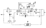
FIG. 1 is a circuit configuration diagram of a conventional DC conversion apparatus. In the DC conversion apparatus shown in FIG. 1, a synchronous rectifier that includes a low on-resistance power MOSFET (Field-Effect Transistor) and the like is used on a secondary side (output side) of a transformer in order to reduce power losses.
In FIG. 1, a MOSFET (Field-Effect Transistor) switch Q1 is connected to a DC power source vdc1 via a primary winding 5 a (the number of turns of n1) of a transformer T1, and a series circuit of a resistor R1 and a capacitor C1 is connected to both ends of the switch Q1. A series circuit of a diode D2 and a capacitor C2 is connected to both ends of the primary winding 5 a of the transformer T1, and a resistor R2 is connected to both ends of the capacitor C2. The switch Q1 is turned ON/OFF by PWM control of a control circuit 10.
The primary winding 5 a of the transformer T1 and a secondary winding 5 b (the number of turns is n2) of the transformer T1 each have a winding structure such that a common mode voltage is generated mutually, and a MOSFET switch Q3 and a MOSFET switch Q4 are connected in series to both ends of the secondary winding 5 b of the transformer T1. One end of the secondary winding 5 b (at filled circle (●) side) of the transformer T1 is connected to a gate of the switch Q4, and the other end thereof is connected to a gate of the switch Q3. The switch Q3 is connected to a diode D3 in parallel, and the switch Q4 is connected to a diode D4 in parallel. These devices form a synchronous rectifying circuit. This synchronous rectifying circuit rectifies a voltage (ON/OFF-controlled pulse voltage) generated at the secondary winding 5 b of the transformer T1 in synchronization with ON/OFF operations of the switch Q1, and outputs a DC voltage.
A smoothing reactor Lo and a smoothing capacitor Co are connected in series to both ends of the switch Q3 to form a smoothing circuit. This smoothing circuit smoothes a rectified output of the synchronous rectifying circuit, and outputs a DC output to a load RL.
The control circuit 10 ON/OFF controls the switch Q1 so that the width of an ON-pulse applied to the switch Q1 is narrowed when the output voltage of the load RL reaches or exceeds a reference voltage. That is, when the output voltage of the load RL reaches or exceeds the reference voltage, the width of the ON-pulse applied to the switch Q1 is narrowed so as to control the output voltage to a constant voltage.
Operations of the DC conversion apparatus thus configured are explained with reference to a timing chart at light load time shown in FIG. 2. In FIG. 2, a drain-source voltage of the switch Q1 is depicted by Q1 v, a drain current of the switch Q1 is depicted by Q1 i, a drain current of the switch Q3 is depicted by Q3 i, a drain current of the switch Q4 is depicted by Q4 i, a drain-source voltage of the switch Q3 is depicted by Q3 v, and a gate voltage signal of the switch Q1 is depicted by Q1 g.
Operations performed under high load are explained first. When the switch Q1 is turned ON by the gate voltage signal Q1 g, the current Q1 i flows through a path passing along Vdc1, 5 a, Q1, and Vdc1. This current Q1 i increases linearly with time.
At this time, since a voltage is generated also at the secondary winding 5 b of the transformer T1, the switch Q4 is turned ON and hence the current Q4 i flows clockwise through a path passing along 5 b, Lo, Co, Q4, and 5 b, so that electric power is supplied to the load RL. The current Q4 i increases linearly with time, whereupon Lo(Io)2/2 of energy is stored in the smoothing reactor Lo. A current flowing into the smoothing rector Lo is depicted by Io.
When the switch Q1 is turned OFF, a reverse voltage is generated at the secondary winding 5 b of the transformer T1, and hence the switch Q4 is turned OFF and the switch Q3 is turned ON. Therefore, the energy stored in the smoothing reactor Lo causes the current Q3 i to flow clockwise through a path passing along Lo, Co, Q3, and Lo, so that electric power is supplied continuously to the load RL.
Subsequently, when the switch Q1 is turned ON, the voltage generated at the secondary winding 5 b is reversed again, therefore the switch Q4 is turned ON and the switch Q3 is turned OFF, and then the similar operations as previously described are performed. Since the current of the smoothing reactor Lo flows continuously in the same direction, this state is called a continuous mode.
On the other hand, when a load current decreases (light load condition), a current of the smoothing reactor Lo flowing therethrough as the switch Q1 is turned OFF (e.g., time t32) becomes zero while the switch Q1 is OFF, but the switch Q3 remains ON. Therefore, the electric charge stored in the smoothing capacitor Co is discharged, and then a current Q3 i′ flows counterclockwise through a path passing along Co, Lo, Q3, and Co, so that the energy is stored in the smoothing reactor Lo.
When the switch Q1 is turned ON at time t33 (same as time t31), the switch Q4 is turned ON and the switch Q3 is turned OFF. Therefore, a current Q4 i′ flows counterclockwise through a path passing along Lo, 5 b, Q4, Co, and Lo from the smoothing reactor Lo. As a result, the energy is finally returned to the DC power source vdc1 on a primary side (input side) via the primary winding 5 a of the transformer T1.
As described above, when a synchronous rectifying circuit is applied to the conventional DC conversion apparatus shown in FIG. 1 or to a switching power source device described in Japanese Patent Application Laid-Open No. 2002-10636, they operate with little loss in a high load state in which a current flows continuously through the smoothing reactor Lo.
SUMMARY OF THE INVENTION
In a light load condition as shown in FIG. 2, however, a current of the smoothing reactor Lo flowing therethrough is not continuous and flows backward in a return mode. When the switch Q3 is OFF, the energy stored in the smoothing reactor Lo is returned to the DC power source vdc1 on the input side via the switch Q4 and the transformer T1.
At this time, delay of an ON-timing of the switch Q4 or high leakage inductance of the transformer T1 generates a large spike voltage SP as shown in FIG. 2, causing a breakdown of devices (synchronous rectifier).
In order to solve this problem, it is necessary to additionally provide a spike voltage absorbing circuit such as an absorber having a combination of the resistor R1 and the capacitor C1, and a combination of the resistor R2 and the capacitor C2. Furthermore, the reverse current is detected to stop the synchronous rectification, or high withstand voltage devices are used. These measures lead to complex circuitry and increased losses.
According to the present invention, a DC conversion apparatus that can offer high efficiency and achieve a size reduction by reducing losses and simplifying the circuitry can be provided.
The present invention adopts following means to solve the above problems. A first technical aspect of the present invention provides a DC conversion apparatus including: a first switch that converts a DC voltage of a DC power source to a high-frequency voltage by being turned ON/OFF via a primary winding of a transformer; a synchronous rectifying circuit that performs synchronous rectification of a high-frequency voltage generated at a secondary winding of the transformer; a smoothing circuit that smoothes a rectified output of the synchronous rectifying circuit by a smoothing reactor and a smoothing capacitor, and outputs a DC voltage; a capacitor that stores via a diode, energy stored in the smoothing reactor due to a current backflow of the synchronous rectifying circuit caused at light load time; a second switch that is turned ON in synchronization with the first switch, and that returns the energy stored in the capacitor via the transformer to a primary side thereof; and a control circuit that turns ON/OFF the first switch.
A second technical aspect of the present invention provides a DC conversion apparatus including: a first switch that converts a DC voltage of a DC power source to a high-frequency voltage by being turned ON/OFF via a primary winding of a transformer; a synchronous rectifying circuit that performs synchronous rectification of a high-frequency voltage generated at a secondary winding of the transformer; a smoothing circuit that smoothes a rectified output of the synchronous rectifying circuit by a smoothing reactor and a smoothing capacitor, and outputs a DC voltage; a capacitor that stores via a diode, energy stored in the smoothing reactor due to a current backflow of the synchronous rectifying circuit caused at light load time; a second switch that is turned ON in synchronization with the first switch, and returns the energy stored in the capacitor via the transformer to a primary side thereof; a series circuit of a third switch and a clamp capacitor, the series circuit being connected to both ends of the primary winding of the transformer or to both ends of the first switch; and a control circuit that turns ON/OFF the first switch and the third switch alternately.
A third technical aspect of the present invention provides the DC conversion apparatus, in addition to the first or the second technical aspect, wherein the smoothing reactor is formed on an auxiliary winding of the transformer, the secondary winding of the transformer is tightly coupled with the primary winding of the transformer, and the auxiliary winding of the transformer is loosely coupled with the primary winding.
A fourth technical aspect of the present invention provides the DC conversion apparatus, in addition to the third technical aspect, wherein the number of turns of the secondary windings of the transformer is the same as that of the auxiliary winding, the secondary winding has a winding phase opposite to that of the primary winding of the transformer, and the auxiliary winding has the same winding phase as that of the primary winding.
A fifth technical aspect of the present invention provides the DC conversion apparatus, in addition to the first to the fourth technical aspects, further including a tertiary winding of the transformer connected to the secondary winding of the transformer in series, wherein the second switch is turned ON by a voltage generated at the tertiary winding of the transformer when the first switch is turned ON, and returns the energy stored in the capacitor via the transformer to the primary side thereof.
A sixth technical aspect of the present invention provides the DC conversion apparatus, in addition to the first to the fifth technical aspects, further including an ON-time setting unit that sets an ON-time of the second switch to be shorter than that of the first switch.
A seventh technical aspect of the present invention provides a DC conversion apparatus including: a first series circuit of a first switch and a second switch, the first series circuit being connected to both ends of a DC power source; a second series circuit of a third switch and a fourth switch, the second series circuit being connected to the both ends of the DC power source; a primary winding of a transformer connected to a junction of the first switch and the second switch, and to a junction of the third switch and the fourth switch; a synchronous rectifying circuit that performs synchronous rectification of high-frequency voltages generated at the secondary winding and the tertiary winding of the transformer by a fifth switch connected to the secondary winding of the transformer and by a sixth switch connected to a tertiary winding that is connected to the secondary winding of the transformer in series; a smoothing circuit that smoothes a rectified output of the synchronous rectifying circuit by a smoothing reactor and a smoothing capacitor, and outputs a DC voltage; a capacitor that stores via a diode, energy stored in the smoothing reactor due to a current backflow of the synchronous rectifying circuit caused at light load time; a seventh switch that is turned ON in synchronization with the first switch and the fourth switch, and returns the energy stored in the capacitor via the transformer to a primary side thereof; and a control circuit that turns ON/OFF the first, the fourth, and the fifth switches, and the second, the third, and the sixth switches, in a mutually complementary manner, and turns ON the seventh switch while the first, the fourth, and the fifth switches are ON at the same time.
BRIEF DESCRIPTION OF THE DRAWINGS
FIG. 1 is a circuit configuration diagram of a conventional DC conversion apparatus;
FIG. 2 is a timing chart of signals at each component of the DC conversion apparatus under light load condition shown in FIG. 1;
FIG. 3 is a circuit configuration diagram of a DC conversion apparatus according to a first embodiment;
FIG. 4 is a timing chart of signal at each component of the DC conversion apparatus under light load condition according to the first embodiment;
FIG. 5 is a circuit configuration diagram of a DC conversion apparatus according to a second embodiment;
FIG. 6 is a diagram of an example of a waveform shaping circuit provided in the DC conversion apparatus according to the second embodiment;
FIG. 7 is a diagram of an operational waveform of the waveform shaping circuit shown in FIG. 6;
FIG. 8 is a timing chart of signal at each component of the DC conversion apparatus under high load condition;
FIG. 9 is a circuit configuration diagram of a DC conversion apparatus according to a third embodiment;
FIG. 10 is a circuit configuration diagram of a DC conversion apparatus according to a fourth embodiment;
FIG. 11 is a configuration diagram of a transformer provided in the DC conversion apparatus according to the fourth embodiment;
FIG. 12 is a timing chart of signal at each component of the DC conversion apparatus according to the fourth embodiment; and
FIG. 13 is a circuit configuration diagram of a DC conversion apparatus according to a fifth embodiment.
DESCRIPTION OF THE PREFERRED EMBODIMENTS
Embodiments of a DC conversion apparatus according to the present invention will be explained in detail below with reference to the drawings. According to the DC conversion apparatus of the embodiments, a spike voltage is eliminated in such that energy stored in a smoothing reactor due to a current backflow under light load condition is transferred to a capacitor via a diode, and the energy is returned to a primary side without any power loss by use of a second switch or a seventh switch (as a switching device) which is turned ON synchronize with turning a first switch on.
First Embodiment
FIG. 3 is a circuit configuration diagram of a DC conversion apparatus according to a first embodiment. The DC conversion apparatus in the first embodiment shown in FIG. 3 is different from the conventional one shown in FIG. 1 in that a transformer T2 is used and in that diodes D5 and D6, a capacitor C5, and a MOSFET switch Q5 (second switch) are additionally provided. Other configurations are the same as those shown in FIG. 1, so like reference signs denote like parts and details thereof will be omitted. Only the different parts will be explained.
The transformer T2 has a primary winding 5 a (the number of turns is n1), a secondary winding 5 b (the number of turns is n2) configured to be tightly coupled with the primary winding 5 a and to have a winding structure such that a common mode voltage is generated, and a tertiary winding 5 c (the number of turns is n3) configured to be tightly coupled with the primary winding 5 a and to have a winding structure such that a common mode voltage is generated. The secondary winding 5 b and the tertiary winding 5 c are connected in series.
A MOSFET switch Q3 and a MOSFET switch Q4 are connected in series to both ends of the secondary winding 5 b of the transformer T2. One end of the secondary winding 5 b (at filled circle (●) side) of the transformer T2 is connected to a gate of the switch Q4, and the other end of the secondary winding 5 b of the transformer T2 is connected to a gate of the switch Q3. The switch Q3 is connected to a diode D3 in parallel, and the switch Q4 is connected to a diode D4 in parallel. These devices form a synchronous rectifying circuit. This synchronous rectifying circuit rectifies a voltage (ON/OFF controlled pulse voltage) generated at the secondary winding 5 b of the transformer T2 in synchronization with ON/OFF operations of a MOSFET switch Q1 (first switch), and a DC voltage is outputted.
The anode of the diode D5 is connected to a junction of the secondary winding 5 b and the tertiary winding 5 c, the cathode of the diode D3, and one end of a smoothing reactor Lo. The cathode of the diode D5 is connected to one end of the capacitor C5, and the other end of the capacitor C5 is connected to one end of the smoothing capacitor Co and the anodes of the diodes D3 and D4. The diode D5 is connected between the source and the drain of the switch Q5, and a gate of the switch Q5 is connected to one end of the tertiary winding 5 c (at filled circle (●) side).
The diode D6 is connected between a joint of the secondary winding 5 b and the cathode of the diode D4 and a joint of the cathode of the diode D5 and the capacitor C5. This diode D6 is provided to suppress a spike voltage, by absorbing the energy of the spike voltage generated at recovery time of the diode D4 in the capacitor C5.
Operations of the DC conversion apparatus of the embodiment are explained with reference to a timing chart for light load condition as shown in FIG. 4. In FIG. 4, a drain-source voltage of the switch Q1 is depicted by Q1 v, a drain current of the switch Q1 is depicted by Q1 i, a drain current of the switch Q3 is depicted by Q3 i, a drain current of the switch Q4 is depicted by Q4 i, a drain current of the switch Q5 is depicted by Q5 i, a drain-source voltage of the switch Q3 is depicted by Q3 v, and a gate voltage signal of the switch Q1 is depicted by Q1 g.
Operations performed under high load condition are explained first. When the switch Q1 is turned ON by the gate voltage signal Q1 g, the current Q1 i flows clockwise through a path passing along Vdc1, 5 a, Q1, and vdc1. This current Q1 i increases linearly with time.
At this time, a voltage is generated also at the secondary winding 5 b of the transformer T2, and hence the switch Q4 is turned ON and the current Q4 i flows clockwise through a path passing along 5 b, Lo, Co, Q4, and 5 b, so that electric power is supplied to a load RL. The current Q4 i also increases linearly with time, whereupon Lo(Io)2/2 of energy is stored in the smoothing reactor Lo. A current flowing through the smoothing reactor Lo is depicted by Io.
When the switch Q1 is turned OFF, the voltage at the secondary winding 5 b of the transformer T2 is reversed, so that the switch Q4 is turned OFF and the switch Q3 is turned ON. Therefore, the energy stored in the smoothing reactor Lo causes the current Q3 i to flow clockwise through a path passing along Lo, Co, Q3, and Lo, and hence electric power is supplied continuously to the load RL.
Subsequently, in a similar manner, when the switch Q1 is turned ON, the voltage of the secondary winding 5 b is reversed again, then the switch Q3 is turned OFF and the switch Q4 is turned ON. This state is called a continuous mode in which the current of the smoothing reactor Lo flows continuously in the same direction.
On the other hand, when a load current decreases (light load condition), a current of the smoothing reactor Lo flowing therethrough when the switch Q1 is turned OFF (e.g., time t2) becomes zero while the switch Q1 is OFF, but the switch Q3 remains ON. Therefore, the electric charge stored in the smoothing capacitor Co is discharged, and then the current Q3 i′ flows counterclockwise through a path passing along Co, Lo, Q3, and Co, so that the energy is stored in the smoothing reactor Lo.
When the switch Q1 is turned ON at time t3 (same as time t1), a voltage at one end of the secondary winding 5 b (at filled circle (●) side) of the transformer T2 is applied to the gate of the switch Q4 thereby turning ON the switch Q4 and turning OFF the switch Q3. Therefore, the energy stored in the smoothing reactor Lo is stored in the capacitor C5 via the diode D5. That is, the diode D5 is activated, and the current Q5 i starts to flow, thereby the energy is stored in the capacitor C5, so that the spike voltage is absorbed.
Since a voltage is generated at one end of the tertiary winding 5 c (at filled circle (●) side) of the transformer T2, this voltage is applied to the gate of the switch Q5, thereby turning ON the switch Q5. Therefore, the current Q5 i′ flows counterclockwise through a path passing along C5, Q5, 5 b, Q4, and C5, and as a consequence, the energy stored in the capacitor C5 is returned to the DC power source vdc1 on the primary side via the secondary winding 5 b and the primary winding 5 a.
As shown in FIG. 4, the voltage Q3 v of the switch Q3 is clamped, so that no spike voltage is generated. Therefore, it is possible to set the withstand voltage of the switch Q3 at a lower value. Accordingly, the use of a low ON-resistance power device leads to a further reduction in losses.
As described above, according to the DC conversion apparatus of the first embodiment, the energy stored in the smoothing rector Lo due to a current backflow caused under light load condition is stored in the capacitor C5 via the diode D5, and by use of the switch Q5 that is tuned ON synchronously as the switch Q1 is ON, the energy is returned to the primary side without any loss, as a result, a spike voltage can be eliminated. Therefore, the withstand voltage of a rectification device can be set at lower levels, and ON-resistance can be reduced by use of a low withstand-voltage device. Furthermore, a C-R absorber for preventing from the spike voltage can be eliminated, so that the circuitry can be simplified.
Second Embodiment
FIG. 5 is a circuit configuration diagram of a DC conversion apparatus according to a second embodiment. The DC conversion apparatus as shown in FIG. 5 has a waveform shaping circuit 11 serving as an ON-time setting unit, between one end of the tertiary winding 5 c of the transformer T2 and the gate of the switch Q5, in addition to the DC conversion apparatus as shown in FIG. 3.
Other configurations shown in FIG. 5 are the same as those shown in FIG. 3, so like reference signs denote like parts and details thereof will be omitted.
The waveform shaping circuit 11 shapes the waveform of a voltage generated at the tertiary winding 5 c of the transformer T2, so as to set the waveform of a drive voltage applied to the gate of the switch Q5 to be shorter than an ON-time of the switch Q1. FIG. 6 shows an example of the waveform shaping circuit 11. The waveform shaping circuit 11 has a time-constant circuit that includes a resistor RT having one end thereof being connected to the tertiary winding 5 c and the other end thereof being connected to the gate of the switch Q5, and a capacitor CT being connected between the other end of the resistor RT and the ground.
The time-constant circuit having the resistor RT and the capacitor CT outputs voltage VCT across the capacitor CT with the waveform linearly increasing with time in response to an input rectangular voltage Vn3 of the tertiary winding 5 c, and the voltage VCT is applied to the gate of the switch Q5 as shown in FIG. 7. As a result, the switch Q5 is turned ON only when the output voltage VCT of the waveform shaping circuit 11 reaches or exceeds a threshold voltage VTH of the gate of the switch Q5. That is, since an ON-time TON during which the switch Q5 is ON is set to be shorter than the ON-time of the switch Q1, the current of the switch Q5 under high load condition can be reduced.
FIG. 8 shows a timing chart of each signal of component under high load condition of the DC conversion apparatus according to the embodiment. As shown in FIG. 8, a broken line IN for the current Q5 i of the switch Q5 corresponds to a case where the waveform shaping circuit 11 is not provided, and a solid line IW corresponds to a case of this embodiment. In the DC conversion apparatus according to this embodiment, it is apparent that the current of the switch Q5 under high load condition decreases due to the waveform shaping circuit 11.
When the switch Q5 is turned ON for the same period of time as the ON-time of the switch Q1 similarly to the first embodiment, a resonance circuit is formed of the capacitor C5 and a leakage inductance between the primary winding 5 a and the secondary winding 5 b of the transformer T2, and a resonance current flows therefrom. According to the second embodiment, the ON-time of the switch Q5 is set to be shorter, and thus the resonance circuit is blocked, so that the resonance current can be reduced.
Third Embodiment
FIG. 9 shows a circuit configuration diagram of a DC conversion apparatus according to a third embodiment. The DC conversion apparatus as shown in FIG. 9 includes a resonance circuit using an active-clamp topology in addition to the DC conversion apparatus of the first embodiment as shown in FIG. 3.
In FIG. 9, the MOSFET switch Q1 (first switch) is connected to the DC power source vdc1 via the primary winding 5 a (the number of turns is n1) of the transformer T2, and the diode D1 and the capacitor C1 are connected in parallel to both ends of the switch Q1. The diode D1 can be a parasitic diode, and the capacitor C1 can have a parasitic capacity.
One end of a MOSFET switch Q2 (third switch) is connected to a junction of one end of the primary winding 5 a of the transformer T2 and one end of the switch Q1, and the other end of the switch Q2 is connected to a positive electrode of the DC power source vdc1 via a clamp capacitor C2. Alternatively, the other end of the switch Q2 can be connected to a negative electrode of the DC power source vdc1 via the clamp capacitor C2.
The diode D2 is connected in parallel to both ends of the switch Q2. The diode D2 can be a parasitic diode of the switch Q2. The switches Q1 and Q2 each have a duration for which they are turned OFF (dead time), and are alternately turned ON/OFF by PWM control of a control circuit 10 a.
The control circuit 10 a alternately turns ON/OFF the switches Q1 and Q2 so that when an output voltage of a load RL reaches or exceeds a reference voltage, the width of an ON-pulse applied to the switch Q1 is narrowed and the width of an ON-pulse applied to the switch Q2 is widened. That is, when the output voltage of the load RL reaches or exceeds the reference voltage, this output voltage is regulated at a constant level by narrowing the ON-pulse width of the switch Q1.
Furthermore, the control circuit 10 a turns ON the switch Q1 during a predetermined period of time after the switch Q1 reaches a zero-voltage condition due to resonance between the capacitor C1 connected to the switch Q1 in parallel, and a leakage inductance (not shown) between the primary winding and the secondary winding of the transformer T2.
Operations of the DC conversion apparatus thus configured according to the third embodiment will be explained. First, operations performed under high load condition are described.
When the switch Q2 is turned OFF, the voltage Q1 v of the switch Q1 decreases due to the resonance of the capacitor C1 and the leakage inductance existing between the primary and the secondary windings of the transformer T2. When the switch Q1 is turned ON while the voltage Q1 v thereof is zero, zero-voltage switching of the switch Q1 is achieved.
Next, when the switch Q1 is turned ON, the current Q1 i flows clockwise through a path passing along vdc1, 5 a, Q1, and vdc1. At this time, since a voltage is generated also at the secondary winding 5 b of the transformer T2, the switch Q4 is turned ON and the current Q4 i flows clockwise through a path passing along 5 b, Lo, Co, Q4, and 5 b, so that electric power is supplied to a load RL. Lo(Io)2/2 of energy is stored in the smoothing reactor Lo at this time.
Subsequently, when the switch Q1 is turned OFF, a current flows due to exciting energy stored in the primary winding 5 a, and then the capacitor C1 is charged. At this time, the leakage inductance between the primary and the secondary windings of the transformer T2 resonates with the capacitor C1, so that the voltage Q1 v of the switch Q1 increases.
When the electrical potential of the switch Q1 reaches that of the clamp capacitor C2, the diode D2 becomes conductive, and the clamp capacitor C2 starts to be charged. At this time, zero-voltage switching of the switch Q2 is achieved by turning ON the switch Q2. Furthermore, the voltage of the secondary winding 5 b of the transformer T2 is reversed, and therefore the switch Q4 is turned OFF and the switch Q3 is turned ON. As a result, the current Q3 i flows clockwise through a path passing along Lo, Co, Q3, and Lo due to the energy stored in the smoothing reactor Lo, so that the electric power is continuously supplied to the load RL.
Next, when the switch Q2 is turned ON, the current Q2 i flows counterclockwise through a path passing along C2, Q2, 5 a, and C2, and finally the energy is returned to the primary winding 5 a.
Since operations under light load condition are performed in the similar manner as those under light load condition according to the first embodiment, the descriptions thereof will be omitted.
As described above, according to the resonant DC conversion apparatus employing the active clamp topology, the leakage inductance between the primary and the secondary windings of the transformer T2 is larger, and the resonance between this leakage inductance and the capacitor C1 is utilized to achieve the zero-voltage switching of the switches Q1 and Q2. As a result, this leakage inductance makes the generation of the spike voltage more remarkable. However, this spike voltage can be eliminated by transferring the energy, that is stored in the smoothing reactor Lo due to a current backflow caused under light load condition, to the capacitor C5 via the diode D5, and returning the energy to the primary side of the transformer T2 without any loss by use of the switch Q5 which is turned ON synchronously when the switch Q1 is ON.
The waveform shaping circuit 11 as shown in FIG. 5 can be additionally provided between one end of the tertiary winding 5 c of the transformer T2 and the gate of the switch Q5 in the DC conversion apparatus as shown in FIG. 9. This achieves a similar advantageous effect as that obtained in the second embodiment.
Fourth Embodiment
FIG. 10 shows a circuit configuration diagram of a DC conversion apparatus according to a fourth embodiment. The DC conversion apparatus shown in FIG. 10 is different from that of the third embodiment shown in FIG. 9 in that a transformer T3 has a primary winding 5 a to a quaternary winding 5 d (corresponding to an auxiliary winding of the present invention in which the number of turns is n4), and in that the primary winding 5 a is loosely coupled with the quaternary winding 5 d and is also tightly coupled with the secondary winding 5 b and the tertiary winding 5 c. When the switch Q1 is ON, DC excitation of the transformer T3 in its operating state is canceled by magnetomotive forces having the same magnitude but in opposite directions at the primary winding 5 a and the quaternary winding 5 d, and when the switch Q1 is OFF, DC excitation of the transformer T3 in its operating state is canceled by magnetomotive forces having the same magnitude but in opposite directions at the secondary winding 5 b and the quaternary winding 5 d so as to increase an exciting inductance, resulting in a reduced exciting current and thus in reduced losses.
The quaternary winding 5 d is provided at a position corresponding to the smoothing reactor Lo shown in FIG. 9. The number of turns of the secondary winding 5 b of the transformer T3 is the same as that of the quaternary winding 5 d of the transformer T3. The secondary winding 5 b of the transformer T3 has a winding phase opposite to that of the primary winding 5 a of the transformer T3, and the tertiary winding 5 c and the quaternary winding 5 d of the transformer T3 have the same winding phase as that of the primary winding 5 a of the transformer T3.
The anode of the diode D5 is connected to a joint of the secondary winding 5 b and the tertiary winding 5 c, the cathode of the diode D4, one end (drain) of the switch Q4, and the gate of the switch Q3. The cathode of the diode D5 is connected to one end of the quaternary winding 5 d via the capacitor C5. Both ends of the diode D5 are connected between the drain and the source of the switch Q5, and the gate of the switch Q5 is connected to one end (at filled circle (●) side) of the tertiary winding 5 c. The diode D6 is connected to one end of the quaternary winding 5 d and one end of the capacitor C5.
Other configurations shown in FIG. 10 are the same as those shown in FIG. 9, so like reference signs denote like parts and details thereof will be omitted.
FIG. 11 is a configuration diagram of the transformer provided in the DC conversion apparatus according to the fourth embodiment. The transformer shown in FIG. 11 includes a core 20 having a rectangular external shape and also having therein oblong apertures 24 a and 24 b that are formed to configure magnetic paths 25 a, 25 b, and 25 c in a longitudinal direction thereof. The primary winding 5 a, the secondary and the tertiary windings 5 b and 5 c closely and tightly coupled with the primary winding 5 a, and the quaternary winding 5 d loosely coupled with the primary winding 5 a are provided in a core part 20 a of the core 20. In order to loosely couple the primary winding 5 a with the quaternary winding 5 d, a projecting portion 20 b is formed between the secondary and the tertiary windings 5 b and 5 c, and the quaternary winding 5 d in the core part 20 a. This projecting portion 20 b works to increase a leakage flux, resulting in a large leakage inductance of the quaternary winding 5 d.
Operations of the DC conversion apparatus thus configured in the embodiment are explained next, with reference to a timing chart shown in FIG. 12. In FIG. 12, a voltage across the switch Q1 is depicted by Q1 v, a current flowing into the switch Q1 is depicted by Q1 i, a current flowing into the switch Q2 is depicted by Q2 i, a current flowing into the diode D2 is depicted by D2 i, and a current flowing into the quaternary winding 5 d of the transformer T3 is depicted by n4 i.
First, operations performed under high load condition are explained. When the switch Q1 is turned ON at time t1, the current Q1 i (equivalent to a current I1 flowing through the primary winding 5 a) flows clockwise through a path passing along vdc1, 5 a, Q1, and vdc1. At the same time, a voltage is generated at the quaternary winding 5 d that is loosely coupled with the primary winding 5 a, and then the current n4 ia (equivalent to a current I1′ corresponding to the current I1) flows clockwise through a path passing along 5 d, Co, Q3, and 5 d, so that electric power is supplied to a load RL. The quaternary winding 5 d has a high leakage inductance as it is loosely coupled with the primary winding 5 a. At this time, a relationship of I1·n1=I1′·n4 according to the law of equal ampere-turns, and hence the DC excitation is canceled.
Next, when the switch Q1 is turned OFF at time t2, a current flows due to exciting energy stored in the primary winding 5 a, and then the capacitor C1 is charged. At this time, a leakage inductance (not shown) of the primary winding 5 a of the transformer T3 resonates with the capacitor C1, and the voltage Q1 v of the switch Q1 increases abruptly.
When the electrical potential of the switch Q1 reaches that of a clamp capacitor C2, the diode D2 becomes conductive, and then the clamp capacitor C2 starts to be charged as the current D2 i (shown in FIG. 12) flows into the diode D2. At this time, zero-voltage switching of the switch Q2 is achieved by turning ON the switch Q2.
Subsequently, the clamp capacitor C2 is completely charged, and the electrical charge stored therein is returned to the primary winding 5 a via the switch Q2. At this time, the filled circle side of the primary winding 5 a is negative, and the non-circle side thereof is positive. Therefore, also on the secondary side of the transformer T3, the filled circle side of the secondary winding 5 b is negative and the non-circle side thereof is positive, and the filled circle side of the quaternary winding 5 d is negative and the non-circle side thereof is positive. Furthermore, the current n4 ib continues to flow clockwise through a path passing along 5 b, 5 d, Co, Q4, and 5 b due to a leakage inductance (not shown) of the quaternary winding 5 d. Therefore, a current always passes through the load RL irrespective of whether the switch Q1 is ON or OFF, so that a ripple current of the smoothing capacitor Co can be reduced.
Since the secondary winding 5 b and the quaternary winding 5 d have the same number of turns and opposite polarities, the magnetomotive forces of the both windings 5 b and 5 d are eliminated and become zero. That is, the DC excitation is canceled.
Accordingly, the impedance on the secondary side of the transformer T3 viewed from the primary side thereof is increased, and when the switch Q2 is turned OFF at time t3 (same as time t1), the current of the switch Q2 is almost enough to discharge the energy in the capacitor C1. Therefore, the electrical potential of the switch Q1 decreases to zero, and then the diode D1 becomes conductive. At this time, zero-voltage switching of the switch Q1 can be achieved by turning ON the switch Q1.
On the other hand, when a load current decreases (during light load condition), a current of the quaternary winding 5 d flowing therethrough when the switch Q2 is turned ON becomes zero while the switch Q2 is ON, but the switch Q4 remains ON. Therefore, the electric charge stored in the smoothing capacitor Co is discharged, and the current n4 ib′ flows counterclockwise through a path passing along Co, 5 d, 5 b, Q4, and Co so that the energy is stored in the quaternary winding 5 d.
Next, when the switch Q2 is turned OFF and also the switch Q1 is turned ON, the switch Q4 is turned OFF and the switch Q3 is turned ON. Therefore, the energy stored in the quaternary winding 5 d is transferred to the capacitor C5 via the diode D5. That is, the diode D5 is activated and the energy is stored in the capacitor C5, so that a spike voltage is absorbed.
Furthermore, since a voltage is generated at one end (at filled circle (●) side) of the tertiary winding 5 c of the transformer T3, this voltage is applied to the gate of the switch Q5 to turn ON the switch Q5. This causes the current Q5 i′ to flow clockwise through a path passing along C5, Q5, 5 b, and C5, and finally the energy stored in the capacitor C5 is returned to the DC power source vdc1 on the primary side via the secondary winding 5 b and the primary winding 5 a.
Therefore, the voltage Q4 v of the switch Q4 is clamped, and therefore no spike voltage is generated. This makes it possible to set the withstand voltage of the switch Q4 at a lower level. Accordingly, since a low ON-resistance power device can be used, the losses can be further reduced.
As described above, according to the DC conversion apparatus of the fourth embodiment, the energy stored in the quaternary winding 5 d due to a current backflow caused under light load condition is transferred to the capacitor C5 via the diode D5, and this energy is returned to the primary side of the transformer T3 without any loss by use of the switch Q5 that is turned ON synchronously when the switch Q1 is ON, so that the spike voltage can be eliminated.
Furthermore, the diode D6 operates to suppress the spike voltage, by absorbing the energy of the spike voltage generated at recovery time of the diode D3 in the capacitor C5. Therefore, a device with a low withstand voltage device can be employed, thereby reducing losses.
The quaternary winding 5 d is provided on the secondary side of the transformer T3, the primary winding 5 a and the quaternary winding 5 d are loosely coupled with each other, and the primary winding 5 a and the secondary winding 5 b are tightly coupled with each other. When the switch Q1 is ON, the DC excitation of the transformer T3 in its operating state is canceled by magnetomotive forces having the same magnitude but in opposite directions at the primary winding 5 a and the quaternary winding 5 d, and when the switch Q1 is OFF, the DC excitation of the transformer T3 in its operating state is canceled by magnetomotive forces having the same magnitude but in opposite directions at the secondary winding 5 b and the quaternary winding 5 d. Therefore, the exciting inductance can be increased, thereby reducing exciting current and thus reducing losses. Furthermore, zero-voltage switching can be achieved, and a compact, highly efficient, and low-noise DC conversion apparatus can be obtained.
In the DC conversion apparatus according to the fourth embodiment shown in FIG. 10, the waveform shaping circuit 11 as shown in FIG. 5 can be provided between one end of the tertiary winding 5 c of the transformer T3 and the gate of the switch Q5. This also offers the same advantageous effect as that obtained in the second embodiment.
In the DC conversion apparatus of the fourth embodiment shown in FIG. 10, a configuration without having an active-clamp circuit on the input side of a transformer, for example, the configuration as shown in FIG. 3, can also be employed.
Fifth Embodiment
FIG. 13 is a circuit configuration diagram of a DC conversion apparatus according to a fifth embodiment. The DC conversion apparatus of the fifth embodiment is an example of the apparatus applied to a push pull circuit. In the first to the fourth embodiments, drive signals of the switches Q3, Q4, and Q5 are self-excitation signals, and are generated by voltages of the secondary winding 5 b and the tertiary winding 5 c. In the fifth embodiment, on the other hand, a control circuit 10 b generates drive signals for the switches Q3, Q4, and Q5.
In FIG. 13, a series circuit of a switch Q1 a (first switch) and a switch Q2 b (second switch), and also a series circuit of a switch Q2 a (third switch) and a switch Q1 b (fourth switch) are connected to both ends of the DC power source vdc1. Both ends of a primary winding 5 a of the transformer T2 are connected to a joint of the switch Q1 a and the switch Q2 b, and also a joint of the switch Q2 a and the switch Q1 b. The switches Q1 a, Q2 a, Q1 b, and Q2 b are connected to diodes D1 a, D2 a, D1 b, D2 b, respectively. The switches Q1 a, Q1 b, Q2 a, and Q2 b each are MOSFET switches. The diodes D1 a, D2 a, D1 b, and D2 b can be parasitic diodes of the switches Q1 a, Q2 a, Q1 b, and Q2 b, respectively.
The switch Q1 a and the switch Q1 b are turned ON or OFF simultaneously with each other by PWM control of the control circuit 10 b, and the switch Q2 a and the switch Q2 b are also turned ON or OFF simultaneously with each other by PWM control of the control circuit 10 b. The switches Q1 a and Q1 b, and the switches Q2 a and Q2 b operate in a mutually complementary manner.
The primary winding 5 a, the secondary winding 5 b, and the tertiary winding 5 c of the transformer T2 each has a winding structure so that a common mode voltage is generated. The secondary winding 5 b and the tertiary winding 5 c are connected in series, and one end (at filled circle (●) side) of the secondary winding 5 b is connected to one end of a MOSFET switch Q3 (fifth switch) and the anode of the diode D3. One end of the tertiary winding 5 c is connected to one end of a MOSFET switch Q4 (sixth switch) and the anode of the diode D4. The other end of the switch Q3 and the cathode of the diode D3 are connected to the other end of the switch Q4 and the cathode of the diode D4.
A series circuit of the smoothing reactor Lo and the smoothing capacitor Co is connected between a joint of the other end of the switch Q3 and the cathode of the diode D3, and a joint of the secondary winding 5 b and the tertiary winding 5 c. A series circuit of the diode D5 and the capacitor C5 is connected between a joint of the other end of the switch Q4 and the cathode of the diode D4, and the joint of the secondary winding 5 b and the tertiary winding 5 c. The diode D5 is connected between the drain and the source of a MOSFET switch Q5 (seventh switch) at both ends of the diode D5.
The control circuit 10 b turns ON or OFF the switches Q1 a, Q1 b, and Q3 at the same time, also turns ON or OFF the switches Q2 a, Q2 b, and Q4 at the same time, and further causes the switches Q1 a, Q1 b, and Q3, and the switches Q2 a, Q2 b, and Q4 to operate in a mutually complementary manner. The control circuit 10 b turns ON the switch Q5 during a period for which the control circuit 10 b turns ON the switches Q1 a, Q1 b, and Q3 at the same time.
Operations of the DC conversion apparatus thus configured in the fifth embodiment will be explained. First, when the switches Q1 a, Q1 b, and Q3 are turned ON simultaneously under high load condition, a current Q1 abi flows through a path passing along vdc1, Q1 a, 5 a, Q1 b, and vdc1. Therefore, on the secondary side of the transformer T2, a current Q3 i flows through a path passing along 5 b, Q3, Lo, Co, and 5 b, so that electric power is supplied to a load RL.
Next, when the switches Q2 a, Q2 b, and Q4 are turned ON simultaneously, a current Q2 abi flows in a reverse direction through a path passing along vdc1, Q2 a, 5 a, Q2 b, and vdc1 into the primary winding 5 a. Therefore, on the secondary side of the transformer T2, a current Q4 i flows through a path passing along 5 c, Q4, Lo, Co, and 5 c, so that electric power is supplied to the load RL.
Therefore, DC power is always supplied to the load RL irrespective of whether the switches Q1 a to Q2 b are ON or OFF. That is, since the switches Q3 and Q4 are operating for full-wave rectification, a ripple current is reduced and an output voltage becomes more stable.
Under light load condition, on the other hand, a current of the smoothing reactor Lo flowing therethrough when the switches Q1 a and Q1 b are turned OFF becomes zero while the switches Q1 a and Q1 b are OFF, but the switch Q4 remains ON. Therefore, the electric charge stored in the smoothing capacitor Co is discharged, and a current Q4 i′ flows through a path passing along Co, Lo, Q4, 5 c, and Co, so that the energy is stored in the smoothing reactor Lo.
Subsequently, when the switches Q1 a and Q1 b are turned ON, the switch Q3 is turned ON and the switch Q4 is turned OFF. Therefore, the energy stored in the smoothing reactor Lo is transferred to the capacitor C5 via the diode D5. That is, the diode D5 is activated and the energy is stored in the capacitor C5, so that a spike voltage is absorbed therein.
Next, when the switch Q5 is turned ON by a signal from the control circuit 10 b while the switches Q1 a, Q1 b, and Q3 are in ON state, a current Q53 i flows through a path passing along C5, Q5, Q3, 5 b, and C5, and finally, the energy stored in the capacitor C5 is returned to the DC power source vdc1 on the primary side via the secondary winding 5 b and the primary winding 5 a.
As described above, according to the DC conversion apparatus of the fifth embodiment, the energy stored in the smoothing rector Lo due to a current backflow caused under light load condition is stored transferred to the capacitor C5 via the diode D5, and by use of the switch Q5 that is tuned ON synchronously when the switches Q1 a and Q1 b are ON, the energy is returned to the primary side of the transformer T2 without any loss, so that the spike voltage can be eliminated. Therefore, the withstand voltage of a rectification device can be lowered, and ON-resistance can be reduced because a device with lower withstand-voltage can be employed. Furthermore, a C-R absorber for preventing the spike voltage can be eliminated, thereby simplifying the circuitry.
ADVANTAGES OF THE INVENTION
According to the present invention, the energy stored in a smoothing reactor due to a current backflow under light load condition is transferred to a capacitor via a diode, and by use of a second switch that is turned ON synchronously when a first switch is ON, the energy is returned to the primary side of a transformer without any loss, so that a spike voltage can be eliminated. Therefore, a required withstand voltage of a device used for a synchronous rectifier can be lowered, so that a device with lower withstand-voltage can be employed. Furthermore, a circuit that causes losses, such as a surge absorber, is not necessary, and therefore losses can be reduced. Accordingly, a highly efficient and small DC conversion apparatus can be obtained.
INDUSTRIAL APPLICABILITY
The present invention is applicable to a switching power source, such as a DC-DC converter and an AC-DC converter.
This application claims benefit of priority under 35USC §119 to Japanese Patent Application No. 2004-381737, filed on Dec. 28, 2004, the entire contents of which are incorporated by reference herein. Although the invention has been described above by reference to certain embodiments of the invention, the invention is not limited to the embodiments described above. Modifications and variations of the embodiments described above will occur to those skilled in the art, in light of the teachings. The scope of the invention is defined with reference to the following claims.

Claims (11)

1. A DC conversion apparatus comprising:
a first switch configured to carry out ON/OFF operations via a primary winding of a transformer to convert a DC voltage provided by a DC power source into high-frequency voltage;
a synchronous rectifying circuit configured to carry out synchronous rectification of a high-frequency voltage generated at a secondary winding of the transformer;
a smoothing circuit having a smoothing reactor and a smoothing capacitor configured to smooth a rectified output of the synchronous rectifying circuit and to output a DC voltage;
a storage capacitor configured to store energy being stored in the smoothing reactor and transferred thereto via a diode due to a current backflow of the synchronous rectifying circuit flowing under a light load condition;
a second switch configured to turn ON in synchronization with the first switch and to return the energy stored in the storage capacitor to the DC power source at a primary side of the transformer via the transformer; and
a control circuit configured to turn ON/OFF the first switch.
2. A DC conversion apparatus comprising:
a first switch configured to carry out ON/OFF operations via a primary winding of a transformer to convert a DC voltage provided by a DC power source into high-frequency voltage;
a synchronous rectifying circuit configured to carry out synchronous rectification of a high-frequency voltage generated at a secondary winding of the transformer;
a smoothing circuit having a smoothing reactor and a smoothing capacitor configured to smooth a rectified output of the synchronous rectifying circuit and outputs a DC voltage;
a storage capacitor configured to store energy being stored in the smoothing reactor and transferred thereto via a diode due to a current backflow of the synchronous rectifying circuit flowing under light load condition;
a second switch configured to turn ON in synchronization with the first switch and to return the energy stored in the storage capacitor to the DC power source at a primary side of the transformer via the transformer;
a series circuit of a third switch and a clamp capacitor, the series circuit being connected to both ends of the primary winding of the transformer or to both ends of the first switch; and
a control circuit configured to alternately turn ON/OFF the first switch and the third switch.
3. The DC conversion apparatus according to claim 1, wherein
the smoothing reactor is formed in an auxiliary winding of the transformer,
the secondary winding of the transformer is tightly coupled with the primary winding of the transformer, and
the auxiliary winding of the transformer is loosely coupled with the primary winding.
4. The DC conversion apparatus according to claim 2, wherein
the smoothing reactor is formed in an auxiliary winding of the transformer,
the secondary winding of the transformer is tightly coupled with the primary winding of the transformer, and
the auxiliary winding of the transformer is loosely coupled with the primary winding.
5. The DC conversion apparatus according to claim 3, wherein
the number of turns of the secondary windings of the transformer is the same as that of the auxiliary winding,
the secondary winding has a winding phase opposite to that of the primary winding of the transformer, and
the auxiliary winding has the same winding phase as that of the primary winding.
6. The DC conversion apparatus according to claim 4, wherein
the number of turns of the secondary windings of the transformer is the same as that of the auxiliary winding,
the secondary winding has a winding phase opposite to that of the primary winding of the transformer, and
the auxiliary winding has the same winding phase as that of the primary winding.
7. The DC conversion apparatus according to claim 1, further comprising:
a tertiary winding of the transformer being connected to the secondary winding of the transformer in series, wherein
the second switch is turned ON by a voltage generated at the tertiary winding of the transformer as the first switch is turned ON, and the energy stored in the storage capacitor is returned to the DC power source at the primary side thereof via the transformer.
8. The DC conversion apparatus according to claim 2, further comprising:
a tertiary winding of the transformer being connected to the secondary winding of the transformer in series, wherein
the second switch is turned ON by a voltage generated at the tertiary winding of the transformer when the first switch is turned ON, and the energy stored in the storage capacitor is returned to the DC power source at the primary side thereof via the transformer.
9. The DC conversion apparatus according to claim 1, further comprising an ON-time setting unit configured to set an ON-time of the second switch to be shorter than that of the first switch.
10. The DC conversion apparatus according to claim 2, further comprising an ON-time setting unit configured to set an ON-time of the second switch to be shorter than that of the first switch.
11. A DC conversion apparatus comprising:
a first series circuit of a first switch and a second switch, the first series circuit being connected to both ends of a DC power source;
a second series circuit of a third switch and a fourth switch, the second series circuit being connected to the both ends of the DC power source;
a primary winding of a transformer being connected to a joint of the first switch and the second switch, and to a joint of the third switch and the fourth switch;
a synchronous rectifying circuit configured to perform synchronous rectification of high-frequency voltages generated at the secondary winding and the tertiary winding of the transformer, the synchronous rectifying circuit having a fifth switch connected to the secondary winding of the transformer, and a sixth switch connected to a tertiary winding that is connected to the secondary winding of the transformer in series;
a smoothing circuit having a smoothing reactor and a smoothing capacitor configured to smooth a rectified output of the synchronous rectifying circuit and outputs a DC voltage;
a storage capacitor configured to store energy being stored in the smoothing reactor and transferred thereto via a diode due to a current backflow of the synchronous rectifying circuit flowing under a light load condition;
a seventh switch configured to return the energy stored in the storage capacitor to a primary side of the transformer via the transformer and to be turned ON in synchronization with the first switch and the fourth switch;
a control circuit configured to turn ON or OFF the first, the fourth, and the fifth switches, and the second, the third, and the sixth switches, in a mutually complementary manner, and to turn ON the seventh switch while the first, the fourth, and the fifth switches are turned ON at the same time.
US11/302,234 2004-12-28 2005-12-14 DC conversion apparatus Expired - Fee Related US7218535B2 (en)

Applications Claiming Priority (2)

Application Number Priority Date Filing Date Title
JP2004381737A JP4434010B2 (en) 2004-12-28 2004-12-28 DC converter
JP2004-381737 2004-12-28

Publications (2)

Publication Number Publication Date
US20060139969A1 US20060139969A1 (en) 2006-06-29
US7218535B2 true US7218535B2 (en) 2007-05-15

Family

ID=36611282

Family Applications (1)

Application Number Title Priority Date Filing Date
US11/302,234 Expired - Fee Related US7218535B2 (en) 2004-12-28 2005-12-14 DC conversion apparatus

Country Status (2)

Country Link
US (1) US7218535B2 (en)
JP (1) JP4434010B2 (en)

Cited By (1)

* Cited by examiner, † Cited by third party
Publication number Priority date Publication date Assignee Title
US20150002081A1 (en) * 2013-06-28 2015-01-01 Robert Bosch Gmbh Hand tool battery including a bridge rectifier

Families Citing this family (6)

* Cited by examiner, † Cited by third party
Publication number Priority date Publication date Assignee Title
JP4434011B2 (en) * 2004-12-28 2010-03-17 サンケン電気株式会社 DC converter
US20070139983A1 (en) * 2005-12-20 2007-06-21 Dell Products L.P. Synchronous switch reverse recovery reduction in buck converters
JP5088386B2 (en) * 2010-01-29 2012-12-05 株式会社村田製作所 Switching power supply
DE102011076573A1 (en) * 2011-05-27 2012-11-29 Robert Bosch Gmbh Snubber circuit for DC-DC converter
JP6286793B2 (en) * 2014-01-24 2018-03-07 株式会社日立情報通信エンジニアリング DC-DC converter, secondary battery charge / discharge system, and control method of DC-DC converter
JP6543121B2 (en) * 2015-07-17 2019-07-10 ローム株式会社 Switching power supply

Citations (5)

* Cited by examiner, † Cited by third party
Publication number Priority date Publication date Assignee Title
US6011903A (en) * 1997-04-25 2000-01-04 Soundesign, L.L.C. Reduced-noise ducted flow hair dryer with multiple impellers and ambient air inlets
US6191964B1 (en) * 1995-05-04 2001-02-20 Lucent Technologies Inc. Circuit and method for controlling a synchronous rectifier converter
JP2002010636A (en) 2000-06-23 2002-01-11 Tdk Corp Switching power supply device
US7038922B2 (en) * 2003-02-18 2006-05-02 Alcatel Direct energy transfer converter
US7057906B2 (en) * 2003-03-11 2006-06-06 Denso Corporation Insulating switching DC/DC converter

Patent Citations (5)

* Cited by examiner, † Cited by third party
Publication number Priority date Publication date Assignee Title
US6191964B1 (en) * 1995-05-04 2001-02-20 Lucent Technologies Inc. Circuit and method for controlling a synchronous rectifier converter
US6011903A (en) * 1997-04-25 2000-01-04 Soundesign, L.L.C. Reduced-noise ducted flow hair dryer with multiple impellers and ambient air inlets
JP2002010636A (en) 2000-06-23 2002-01-11 Tdk Corp Switching power supply device
US7038922B2 (en) * 2003-02-18 2006-05-02 Alcatel Direct energy transfer converter
US7057906B2 (en) * 2003-03-11 2006-06-06 Denso Corporation Insulating switching DC/DC converter

Non-Patent Citations (2)

* Cited by examiner, † Cited by third party
Title
U.S. Appl. No. 11/302,184, filed Dec. 14, 2005, Tsuruya, et al.
U.S. Appl. No. 11/302,234, filed Dec. 14, 2005, Tsuruya.

Cited By (2)

* Cited by examiner, † Cited by third party
Publication number Priority date Publication date Assignee Title
US20150002081A1 (en) * 2013-06-28 2015-01-01 Robert Bosch Gmbh Hand tool battery including a bridge rectifier
US9722441B2 (en) * 2013-06-28 2017-08-01 Robert Bosch Gmbh Hand tool battery including a bridge rectifier

Also Published As

Publication number Publication date
JP2006191706A (en) 2006-07-20
JP4434010B2 (en) 2010-03-17
US20060139969A1 (en) 2006-06-29

Similar Documents

Publication Publication Date Title
US7196913B2 (en) DC conversion apparatus
US9118259B2 (en) Phase-shifted dual-bridge DC/DC converter with wide-range ZVS and zero circulating current
US7548435B2 (en) Zero-voltage-switching DC-DC converters with synchronous rectifiers
US5946200A (en) Circulating current free type high frequency soft switching pulsewidth modulated full bridge DC/DC converter
US6947297B2 (en) Active resonant snubber for DC-DC converter
US9124190B2 (en) Isolated switched mode power supply
US20050243579A1 (en) Power system having multiple power converters with reduced switching loss
US7324355B2 (en) Dc-DC converter
US9356526B2 (en) DC-DC power conversion apparatus and method
US9362831B2 (en) Fly-forward converter with energy recovery snubber
US8619438B2 (en) Resonant converter
US7218535B2 (en) DC conversion apparatus
EP3163735B1 (en) Switching power supply unit
US6906931B1 (en) Zero-voltage switching half-bridge DC-DC converter topology by utilizing the transformer leakage inductance trapped energy
US6487094B1 (en) High efficiency DC-DC power converter
KR101140336B1 (en) Isolated buck-boost dc-dc converter
Jeong High efficiency asymmetrical half-bridge converter using a self-driven synchronous rectifier
Jeong High efficiency asymmetrical half-bridge flyback converter using a new voltage-driven synchronous rectifier
US20110310638A1 (en) Power factor corrector and driving method thereof
US11641165B2 (en) Flyback converter and method of operating the same
EP3748834B1 (en) Power supply device
CN115566904A (en) Power conversion circuit
US11632051B2 (en) Flyback converter and method of operating the same
US20240128884A1 (en) Switching control unit, electric power conversion apparatus, and electric power supply system
Qian et al. Self-driven synchronous rectification scheme for wide range application of DC/DC converters with symmetrically driven transformers

Legal Events

Date Code Title Description
AS Assignment

Owner name: SANKEN ELECTRIC CO., LTD., JAPAN

Free format text: ASSIGNMENT OF ASSIGNORS INTEREST;ASSIGNOR:TSURUYA, MAMORU;REEL/FRAME:017363/0569

Effective date: 20051201

STCF Information on status: patent grant

Free format text: PATENTED CASE

FPAY Fee payment

Year of fee payment: 4

FEPP Fee payment procedure

Free format text: PAYOR NUMBER ASSIGNED (ORIGINAL EVENT CODE: ASPN); ENTITY STATUS OF PATENT OWNER: LARGE ENTITY

FPAY Fee payment

Year of fee payment: 8

FEPP Fee payment procedure

Free format text: MAINTENANCE FEE REMINDER MAILED (ORIGINAL EVENT CODE: REM.); ENTITY STATUS OF PATENT OWNER: LARGE ENTITY

LAPS Lapse for failure to pay maintenance fees

Free format text: PATENT EXPIRED FOR FAILURE TO PAY MAINTENANCE FEES (ORIGINAL EVENT CODE: EXP.); ENTITY STATUS OF PATENT OWNER: LARGE ENTITY

STCH Information on status: patent discontinuation

Free format text: PATENT EXPIRED DUE TO NONPAYMENT OF MAINTENANCE FEES UNDER 37 CFR 1.362

FP Lapsed due to failure to pay maintenance fee

Effective date: 20190515