US7205193B2 - Semiconductor device and method for fabricating the same - Google Patents
Semiconductor device and method for fabricating the same Download PDFInfo
- Publication number
- US7205193B2 US7205193B2 US11/024,733 US2473304A US7205193B2 US 7205193 B2 US7205193 B2 US 7205193B2 US 2473304 A US2473304 A US 2473304A US 7205193 B2 US7205193 B2 US 7205193B2
- Authority
- US
- United States
- Prior art keywords
- conductive type
- trench
- storage electrode
- forming
- film
- Prior art date
- Legal status (The legal status is an assumption and is not a legal conclusion. Google has not performed a legal analysis and makes no representation as to the accuracy of the status listed.)
- Expired - Fee Related
Links
- 239000004065 semiconductor Substances 0.000 title claims abstract description 120
- 238000000034 method Methods 0.000 title claims abstract description 63
- 238000003860 storage Methods 0.000 claims abstract description 111
- 239000000758 substrate Substances 0.000 claims abstract description 71
- 239000003990 capacitor Substances 0.000 claims abstract description 50
- 238000002955 isolation Methods 0.000 claims abstract description 38
- 230000001681 protective effect Effects 0.000 claims description 11
- 229910021421 monocrystalline silicon Inorganic materials 0.000 claims description 3
- 238000000151 deposition Methods 0.000 claims description 2
- 239000010410 layer Substances 0.000 description 70
- 230000008569 process Effects 0.000 description 44
- 150000004767 nitrides Chemical class 0.000 description 27
- 238000009792 diffusion process Methods 0.000 description 14
- 229910021420 polycrystalline silicon Inorganic materials 0.000 description 13
- 229920005591 polysilicon Polymers 0.000 description 13
- 238000005229 chemical vapour deposition Methods 0.000 description 11
- 229920002120 photoresistant polymer Polymers 0.000 description 9
- 230000003647 oxidation Effects 0.000 description 8
- 238000007254 oxidation reaction Methods 0.000 description 8
- 238000004519 manufacturing process Methods 0.000 description 7
- 125000006850 spacer group Chemical group 0.000 description 7
- 239000000126 substance Substances 0.000 description 7
- 238000001020 plasma etching Methods 0.000 description 5
- 238000007517 polishing process Methods 0.000 description 5
- 150000002500 ions Chemical class 0.000 description 4
- XUIMIQQOPSSXEZ-UHFFFAOYSA-N Silicon Chemical compound [Si] XUIMIQQOPSSXEZ-UHFFFAOYSA-N 0.000 description 3
- 230000015572 biosynthetic process Effects 0.000 description 3
- 238000005530 etching Methods 0.000 description 3
- 239000012535 impurity Substances 0.000 description 3
- 238000004518 low pressure chemical vapour deposition Methods 0.000 description 3
- 238000012856 packing Methods 0.000 description 3
- 238000005498 polishing Methods 0.000 description 3
- 230000009467 reduction Effects 0.000 description 3
- 229910052710 silicon Inorganic materials 0.000 description 3
- 239000010703 silicon Substances 0.000 description 3
- 238000001039 wet etching Methods 0.000 description 3
- BPQQTUXANYXVAA-UHFFFAOYSA-N Orthosilicate Chemical compound [O-][Si]([O-])([O-])[O-] BPQQTUXANYXVAA-UHFFFAOYSA-N 0.000 description 2
- NBIIXXVUZAFLBC-UHFFFAOYSA-N Phosphoric acid Chemical compound OP(O)(O)=O NBIIXXVUZAFLBC-UHFFFAOYSA-N 0.000 description 2
- 238000001312 dry etching Methods 0.000 description 2
- 239000012212 insulator Substances 0.000 description 2
- 239000011229 interlayer Substances 0.000 description 2
- 239000002184 metal Substances 0.000 description 2
- 238000012986 modification Methods 0.000 description 2
- 230000004048 modification Effects 0.000 description 2
- UPSOBXZLFLJAKK-UHFFFAOYSA-N ozone;tetraethyl silicate Chemical compound [O-][O+]=O.CCO[Si](OCC)(OCC)OCC UPSOBXZLFLJAKK-UHFFFAOYSA-N 0.000 description 2
- 239000005368 silicate glass Substances 0.000 description 2
- KRHYYFGTRYWZRS-UHFFFAOYSA-N Fluorane Chemical compound F KRHYYFGTRYWZRS-UHFFFAOYSA-N 0.000 description 1
- 229910000147 aluminium phosphate Inorganic materials 0.000 description 1
- 239000013078 crystal Substances 0.000 description 1
- 230000008021 deposition Effects 0.000 description 1
- 229960002050 hydrofluoric acid Drugs 0.000 description 1
- 230000003071 parasitic effect Effects 0.000 description 1
- 238000002161 passivation Methods 0.000 description 1
- 238000001259 photo etching Methods 0.000 description 1
- 230000008685 targeting Effects 0.000 description 1
- 238000005019 vapor deposition process Methods 0.000 description 1
Images


Classifications
-
- H—ELECTRICITY
- H10—SEMICONDUCTOR DEVICES; ELECTRIC SOLID-STATE DEVICES NOT OTHERWISE PROVIDED FOR
- H10B—ELECTRONIC MEMORY DEVICES
- H10B12/00—Dynamic random access memory [DRAM] devices
- H10B12/01—Manufacture or treatment
- H10B12/02—Manufacture or treatment for one transistor one-capacitor [1T-1C] memory cells
- H10B12/03—Making the capacitor or connections thereto
- H10B12/038—Making the capacitor or connections thereto the capacitor being in a trench in the substrate
- H10B12/0387—Making the trench
-
- H—ELECTRICITY
- H10—SEMICONDUCTOR DEVICES; ELECTRIC SOLID-STATE DEVICES NOT OTHERWISE PROVIDED FOR
- H10B—ELECTRONIC MEMORY DEVICES
- H10B12/00—Dynamic random access memory [DRAM] devices
- H10B12/30—DRAM devices comprising one-transistor - one-capacitor [1T-1C] memory cells
- H10B12/37—DRAM devices comprising one-transistor - one-capacitor [1T-1C] memory cells the capacitor being at least partially in a trench in the substrate
-
- H—ELECTRICITY
- H10—SEMICONDUCTOR DEVICES; ELECTRIC SOLID-STATE DEVICES NOT OTHERWISE PROVIDED FOR
- H10D—INORGANIC ELECTRIC SEMICONDUCTOR DEVICES
- H10D1/00—Resistors, capacitors or inductors
- H10D1/01—Manufacture or treatment
- H10D1/045—Manufacture or treatment of capacitors having potential barriers, e.g. varactors
- H10D1/047—Manufacture or treatment of capacitors having potential barriers, e.g. varactors of conductor-insulator-semiconductor capacitors, e.g. trench capacitors
-
- H—ELECTRICITY
- H10—SEMICONDUCTOR DEVICES; ELECTRIC SOLID-STATE DEVICES NOT OTHERWISE PROVIDED FOR
- H10D—INORGANIC ELECTRIC SEMICONDUCTOR DEVICES
- H10D86/00—Integrated devices formed in or on insulating or conducting substrates, e.g. formed in silicon-on-insulator [SOI] substrates or on stainless steel or glass substrates
- H10D86/201—Integrated devices formed in or on insulating or conducting substrates, e.g. formed in silicon-on-insulator [SOI] substrates or on stainless steel or glass substrates the substrates comprising an insulating layer on a semiconductor body, e.g. SOI
Definitions
- the present invention relates to semiconductor devices, and more particularly, to a semiconductor device and a method for fabricating the same.
- FIG. 1 illustrates a section of a related art memory having cells each with a transistor and a capacitor.
- a semiconductor device is provided with a semiconductor substrate 1 having a field region FR and an active region AR defined by an active cell isolation film 2 .
- the active region AR of the semiconductor substrate 1 there are a transistor 10 for selective switching of a charge flow and a capacitor 20 for storage of charges switched by the transistor 10 , both of which are arranged related to each other.
- the transistor 10 has a gate insulating film pattern 11 , a gate electrode pattern 12 , spacers 13 , and source/drain diffusion layers 14 , and the storage capacitor 20 has a storage dielectric film 21 and a storage electrode 22 .
- the storage dielectric film 21 and the storage electrode 22 of the capacitor 20 are formed in a trench in the semiconductor substrate 1 , with a portion 22 a of the storage electrode 22 exposed from a surface of the semiconductor substrate 1 , so as to be in electrical contact with the source/drain diffusion layer 14 .
- the related art semiconductor device has the following problems. Although a device packing density has been enhanced by forming the capacitor in the trench of the semiconductor substrate in the active region AR, because the trench is formed in the active region, the capacitor is formed within an area of the active region AR of the semiconductor device. This imposes a limit on increasing the capacitance of the capacitor. Moreover, since there is a limit on the reduction of the active region AR of the semiconductor device, there is a limit on the fabrication of a high density semiconductor device package.
- the present invention is directed to a semiconductor device and a method for fabricating the same that substantially obviates one or more problems due to limitations and disadvantages of the related art.
- the present invention advantageously provides a semiconductor device and a method for fabricating the same in which a capacitor is formed in an active cell isolation trench in a field region.
- a semiconductor device includes a first conductive type semiconductor substrate having an active region and a field region defined thereon, and a trench formed in the field region, a storage dielectric film on an inside surface of the trench, a storage electrode of a capacitor in the trench having the dielectric film formed therein, an active cell isolation film in the trench on the storage electrode, and a transistor on the semiconductor substrate in the active region, the transistor having gate and a source and/or drain regions formed such that the source and/or drain region is electrically connected to the storage electrode.
- the storage electrode includes a first storage electrode in the trench having the dielectric film formed therein, and a second storage electrode for electrically connecting the source and/or drain region of the transistor and the first storage electrode.
- the semiconductor device further includes a second conductive type well in the semiconductor substrate in the active region.
- the semiconductor substrate is a Silicon On Insulator substrate having a buried oxide film.
- a semiconductor device in another aspect of the present invention, includes a first conductive type semiconductor substrate having an active region and a field region defined thereon, and a trench formed in the field region, a storage dielectric film on an inside surface of the trench, a first storage electrode of a capacitor in the trench having the dielectric film formed therein, a protective film on the first storage electrode, a second conductive type epitaxial layer on an entire surface of the first conductive type semiconductor substrate, an active cell isolation film in the field region of the second conductive type epitaxial layer, a transistor on the second conductive type epitaxial layer in the active region, an open trench formed by selectively removing the second conductive type epitaxial layer adjacent to the active cell isolation film and the protective film, and a second storage electrode in the open trench to connect the source and/or drain region of the transistor and the first storage electrode.
- a method for fabricating a semiconductor device includes the steps of forming a trench in a field region of a first conductive type semiconductor substrate, the first conductive type semiconductor substrate having an active region and the field region defined thereon, forming a storage dielectric film on an inside wall of the trench, forming a storage electrode in the trench, forming an active cell isolation film in the trench on the storage electrode, and forming a transistor on the semiconductor substrate in the active region, the transistor formed to have a gate and a source and/or drain region such that the source and/or drain region is electrically connected to the storage electrode.
- a method for fabricating a semiconductor device includes the steps of forming a trench in a field region of a first conductive type semiconductor substrate, the first conductive type semiconductor substrate having an active region and the field region defined thereon, forming a storage dielectric film on an inside surface of the trench, forming a first storage electrode in the trench, forming a protective film on the first storage electrode, forming a second conductive type epitaxial layer on an entire surface of the first conductive type semiconductor substrate, forming an active cell isolation trench in the field region of the second conductive type epitaxial layer, forming an active cell isolation film in the active cell isolation trench, forming an open trench in the second conductive type epitaxial layer adjacent to the active cell isolation film to expose the first storage electrode, forming a second storage electrode in the open trench, the second storage electrode connected to the first storage electrode, and forming a transistor on the second conductive type epitaxial layer in the active region such that the source and/or drain region is connected to the second storage electrode.
- FIG. 1 illustrates a section of a related art memory having cells each with a transistor and a capacitor
- FIG. 2 illustrates a section of a semiconductor device in accordance with a first embodiment of the present invention
- FIGS. 3A–3L illustrate sections showing the steps of a method for fabricating a semiconductor device in accordance with a first embodiment of the present invention
- FIG. 4 illustrates a section of a semiconductor device in accordance with a second embodiment of the present invention
- FIG. 5 illustrates a section of a semiconductor device in accordance with a third embodiment of the present invention.
- FIGS. 6A–6K illustrate sections showing the steps of a method for fabricating a semiconductor device in accordance with a third embodiment of the present invention.
- FIG. 2 illustrates a section of a semiconductor device in accordance with a first exemplary embodiment of the present invention, having cells each with a transistor and a capacitor.
- the semiconductor device includes a first conductive type (for an example, an n type) semiconductor substrate 31 having a field region FR and an active region AR defined by an active cell isolation film 42 .
- a transistor 50 for selective switching of a charge flow.
- a capacitor 46 formed in the semiconductor substrate at a lower portion of the active cell isolation film 42 in the field region FR of the semiconductor substrate 31 .
- a second conductive type for an example, a p type
- the transistor 50 includes a gate insulating film pattern 51 and a gate electrode pattern 52 on the second conductive type well 32 in the first conductive type semiconductor substrate 31 , spacers 53 at sides of the gate electrode pattern 52 , and first conductive type (for example, an n type) source/drain diffusion layers 54 in the second conductive type well 32 on opposite sides of the gate electrode pattern 52 .
- first conductive type for example, an n type
- the capacitor 46 includes a trench 41 in the semiconductor substrate 31 , a storage dielectric film 44 on an inside surface 41 a of the trench 41 , a first storage electrode 43 , and a second storage electrode 45 filled in a portion of a space of the trench 41 so as to be connected to the source/drain diffusion layer 54 of the transistor 50 .
- the active cell isolation film 42 is in the rest of the trench 41 at the upper portion of the capacitor 46 .
- the first storage electrode 43 is surrounded by the storage dielectric film 44 in the trench 41 .
- a second storage electrode 45 on an inside surface 41 a of the trench 41 is supported on the first storage electrode 43 .
- the second storage electrode 45 is electrically connected to the source/drain diffusion layer 54 of the transistor 50 and the first storage electrode 43 .
- the second storage electrode 45 is electrically isolated from the substrate by the storage dielectric film 44 .
- a required area of the active region AR of the semiconductor substrate 31 can be substantially reduced in proportion to an area of the capacitor. That is, because the related art trench type capacitor occupies a portion of the active region, the required area of the active region of the semiconductor device must increase as much as the area occupied by the capacitor. Since the present invention can reduce the active region of the semiconductor device, fabrication of a high density device package is possible. Moreover, the trench type capacitor avoids a step height increase while a size of the active region AR is maintained to a minimum.
- FIGS. 3A–3L illustrate sections showing the steps of a method for fabricating a semiconductor device in accordance with a first embodiment of the present invention.
- second conductive type impurity ions are selectively injected into a first conductive type semiconductor substrate 31 at a transistor region.
- the ions are diffused to form a second conductive type well 32 .
- a high temperature thermal oxidation process is performed to grow a sacrificial oxide film 61 on an entire surface of the first conductive type semiconductor substrate 31 of, for example single crystal silicon, to a thickness in a range of about 120 ⁇ to about 170 ⁇ .
- the sacrificial oxide film 61 moderates stress to the semiconductor substrate 31 applied from a sacrificial nitride film 62 formed later.
- a low pressure chemical vapor deposition process is performed to form the sacrificial nitride film 62 on the sacrificial oxide film 61 to a thickness in a range of about 2000 ⁇ to about 5000 ⁇ .
- the sacrificial nitride film 62 serves as a mask layer in formation of the trench 41 later, and as an etch stop film during chemical-mechanical polishing.
- a first photoresist film pattern 77 is formed on the sacrificial nitride film 62 to expose the sacrificial nitride film 62 in the field region FR of the semiconductor substrate 31 .
- a dry etching process (for an example, a reactive ion etching process) having an anisotropic characteristic is performed by using the first photoresist pattern 77 as a mask.
- the sacrificial oxide film 61 and the sacrificial nitride film 62 are selectively removed to expose the semiconductor substrate 31 in the field region FR. Then, the first photoresist pattern 77 is removed.
- a reactive ion etching process is performed by using the remaining sacrificial oxide film 61 and sacrificial nitride film 62 as a mask.
- the exposed semiconductor substrate 31 is etched in the field region FR anisotropically to a depth in a range of about 6000 ⁇ to about 12000 ⁇ to form an active cell isolation trench 41 .
- a thermal oxidation process is performed at a temperature ranging from about 800° C. to about 900° C.
- a storage dielectric film 44 is formed on an inside surface 41 a of the trench 41 in the semiconductor substrate 31 with a thickness ranging from about 100 ⁇ to about 400 ⁇ .
- a chemical vapor deposition process is performed to form a first polysilicon layer 43 a on an entire surface of the semiconductor substrate 31 to cover the sacrificial nitride film 62 and substantially fill the trench.
- a chemical mechanical polishing process is performed to remove the first polysilicon layer 43 a until a surface of the sacrificial nitride film 62 is exposed. The surface is smoothed. The smoothed first polysilicon layer 43 a is etched back to form a first storage electrode 43 surrounded by the storage dielectric film 44 and filled in a lower space of the trench 41 .
- the storage electrode 43 has a thickness of about 5000 ⁇ to about 8000 ⁇ .
- a second photoresist pattern 78 is formed on the first storage electrode in the trench 41 .
- the second photoresist film pattern 78 is formed to expose some of an upper portion of the storage dielectric film 44 .
- wet etching is performed with HF solution to selectively remove the storage dielectric film 44 exposed from the second photoresist film 78 .
- a portion of the inside surface 41 a of the trench 41 is exposed.
- the exposed inside surface 41 e of the trench 41 is a portion in which a second storage electrode is to be formed.
- the second storage electrode connects the source/drain active layers of the transistor to be formed later and the first storage electrode 43 . Then, the second photoresist film pattern 78 is removed.
- chemical vapor deposition is performed to form a second polysilicon layer 45 a on an entire surface of the semiconductor substrate 31 inclusive of the trench 41 .
- a third photoresist film pattern 79 is formed on the second polysilicon layer 45 a to cover the active region AR of the semiconductor substrate 31 and a portion of the trench 41 on an active region side.
- the second polysilicon layer 45 a is removed selectively by using the third photoresist film pattern 79 as a mask.
- the second polysilicon layer 45 a is left in the active region AR of the semiconductor substrate 31 and only at a portion of the trench on an active region AR side.
- an etch back process is performed targeting the second polysilicon layer 45 a , to form a second storage electrode 45 on the inside surface 41 a of the trench electrically connected to the first storage electrode 43 .
- the second storage electrode 45 has a thickness of about 500 ⁇ to about 1000 ⁇ .
- the second storage electrode 45 is electrically connected to a source/drain diffusion layer 54 of the transistor to be formed later.
- an ozone-TEOS (Tetra Ortho Silicate Glass) process is performed selectively to form an oxide film on the sacrificial nitride film 62 to substantially fill the trench 41 .
- a chemical mechanical polishing process is performed until a surface of the sacrificial nitride film 62 is exposed. The surface is smoothed. Then, the smooth oxide film is subjected to an anisotropic etching to remove a predetermined thickness to form an active cell isolation film 42 which fills rest of the trench 41 .
- a wet etching process is performed with a phosphoric acid solution to remove the sacrificial nitride film 62 entirely.
- a wet etching process is performed with a fluoric acid solution to remove the sacrificial oxide film 61 entirely.
- fabrication is completed of a structure including a capacitor 46 filling a portion of an inside space of the trench 41 in the semiconductor substrate 31 and an active cell isolation film 42 filling rest of the trench for isolating active cells.
- a thermal oxidation process is performed to form a gate insulating film on the first conductive type semiconductor substrate 31 in the active region AR.
- a chemical vapor deposition process is performed to form a conductive layer for forming a gate electrode on the gate insulating film.
- a photoetching process is performed to pattern the gate insulating film and the conductive layer.
- a gate insulating film pattern 51 and a gate electrode pattern 52 are formed on the second conductive type well 32 .
- a series of chemical vapor deposition processes are performed to form an oxide film and a nitride film on an entire surface of the semiconductor substrate inclusive of the gate electrode pattern 52 in succession.
- a dry etching process or a reactive ion etching process, having an anisotropic etching characteristic is performed to etch the oxide film and the nitride film to form spacers 53 at opposite sidewall of the gate electrode pattern 52 .
- first conductive type (for an example, an n type) impurity ions are injected into the second conductive type well 32 in the semiconductor substrate 31 by using the spacers 53 and the gate electrode pattern 52 as a mask to form source/drain diffusion layer 54 on opposite sides of the gate electrode pattern 52 .
- the source/drain diffusion layer 54 is in electrical contact with the second storage electrode 45 of the capacitor 46 spontaneously through the inside surface 41 a of the trench 41 .
- the capacitor 46 stores charges switched by the transistor 50 securely even if the capacitor 46 is in the trench 41 buried under the active cell isolation film 42 .
- the first conductive type semiconductor substrate 31 is used as a common electrode, and the dielectric film 44 and the first storage electrode 43 compose the capacitor.
- FIG. 4 illustrates a section of a semiconductor device in accordance with a second exemplary embodiment of the present invention.
- the capacitor under the active cell isolation film 42 may be formed in an SOI substrate (Silicon On Insulator substrate) having a buried oxide film 81 .
- SOI substrate Silicon On Insulator substrate
- the completed semiconductor device can achieve improved active cell isolation performance, reduction of parasitic capacitance, and so on, more easily.
- the capacitor is formed, not in the active region AR of the semiconductor substrate, but in the field region FR of the semiconductor substrate (i.e., in the active cell isolation trench 41 ), an area of the active region AR of the semiconductor device is reduced to a minimum.
- the completed semiconductor device can meet the requirement for the high density device packing with flexibility.
- Other aspects of the second embodiment are similar to the corresponding aspects of the first embodiment.
- a trench type capacitor may be formed in a first conductive type semiconductor substrate, and by epitaxial growth, or single crystal layer deposition, a second conductive type epitaxial layer may be formed on the first conductive semiconductor substrate to form a transistor.
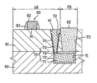
- FIG. 5 illustrates a section of a semiconductor device in accordance with a third exemplary embodiment of the present invention.
- FIGS. 6A–6K illustrate sections showing the steps of a method for fabricating a semiconductor device in accordance with a third exemplary embodiment of the present invention.
- the semiconductor device includes a first conductive type (for an example, an n type) semiconductor substrate 60 having a field region FR and an active region AR defined thereon. There is a trench T 1 in the field region FR. Formed in the trench T 1 in the first conductive type semiconductor substrate 60 , there is a capacitor 70 . A second conductive type (for an example, a p type) epitaxial layer 61 is formed on an entire surface of the first conductive type semiconductor substrate 60 inclusive of the capacitor.
- the active region AR of the second conductive type epitaxial layer 61 there is a transistor 80 for switching a charge flow selectively.
- a second storage electrode 73 for connecting the active cell isolation film 62 , the source/drain diffusion layer of the transistor 80 , and the capacitor 70 .
- the transistor 80 includes a gate insulating film pattern 81 and a gate electrode pattern 82 on the second conductive type epitaxial layer 61 in the active region AR, spacers 83 at sides of the gate electrode pattern 82 , and first conductive type (for an example, an n type) source/drain diffusion layer in the second conductive type epitaxial layer on opposite sides of the gate electrode pattern 82 .
- first conductive type for an example, an n type
- the capacitor 70 includes a dielectric storage film 72 on an inside surface of the trench T 1 , and a first storage electrode 71 in the trench T 1 having the storage dielectric film 72 formed thereon.
- the second storage electrode 73 electrically connects the first storage electrode 71 of the capacitor 70 to the source/drain diffusion layer 84 of the transistor 80 .
- the second storage electrode 73 is electrically isolated from the second conductive epitaxial layer 61 by the insulating film 75 .
- On a surface of the first storage electrode 71 there is a passivation film 74 of nitride formed additionally for preventing damage to the first storage electrode 71 .
- the capacitor 70 is formed in the field region and first conductive type semiconductor substrate 60 is used as a common electrode of the capacitor 70 , a requirement for an area of the active region AR of the semiconductor substrate 60 can be substantially reduced by an area of the capacitor. That is, because the trench type capacitor in the related art occupies a portion of the active region, a required area of the active region of the semiconductor device must increase significantly as much as the occupied area of the capacitor if no other measure is taken. Since the present invention can reduce the active region of the semiconductor device, fabrication of a high density device package is possible. Moreover, the trench type capacitor avoids damage caused by step height increases, while maintaining an area of the active region AR to a minimum.
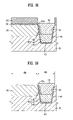
- a first conductive type semiconductor substrate 60 such as single crystal silicon, or so on, is etched selectively, to form a trench T 1 in a field region.
- the trench T 1 has adequate size and depth so that a storage dielectric film and a storage electrode to be formed later have good charge storage capability.
- a thermal oxidation process, a low pressure chemical vapor deposition process, or the like is performed selectively to form an oxide film 72 a for a storage dielectric film on an entire surface of the first conductive type semiconductor substrate 60 inclusive of the trench T 1 , with a thickness in a range of about 100 ⁇ to about 1000 ⁇ .
- a first storage electrode 71 is formed in the trench T 1 .
- a nitride film is formed on the oxide film 72 a inclusive of the first storage electrode 71 .
- the nitride film and the oxide film 72 a are polished by a chemical mechanical polishing process until substantially flush with a surface of the first conductive type semiconductor substrate 60 .
- a capacitor 70 is thus formed.
- the protective film 74 protects the first storage electrode 71 from following process environments.
- a second conductive type epitaxial layer 61 is formed by an epitaxial process, or a second conductive type silicon layer is deposited.
- an epitaxial layer 61 is formed on the first conductive type semiconductor substrate 60 inclusive of the capacitor 70 and the protective film 74 .
- a chemical mechanical polishing process, an etch back process, or the like is performed selectively to smooth the epitaxial layer 61 .
- the epitaxial layer 61 is formed to have a thickness in a range of about 3000 ⁇ to about 8000 ⁇ , so that a transistor formed in a following process is satisfactorily operative.
- a high temperature thermal oxidation process and a low pressure vapor deposition process are performed to form a sacrificial oxide film 101 and a sacrificial nitride film 102 on the second conductive type epitaxial layer. Then, the sacrificial oxide film 101 and the sacrificial nitride film 102 are removed selectively to expose the second conductive type epitaxial layer 61 in the field region FR.
- a reactive ion etching process is performed by using the patterned sacrificial oxide film 10 , and the patterned sacrificial nitride film 102 as a mask.
- the exposed second conductive type epitaxial layer 61 is etched in the field region FR anisotropically to a depth in a range of about 6000 ⁇ to about 12000 ⁇ to form an active cell isolation trench T 3 .
- the active cell isolation trench T 3 is in the second conductive type epitaxial layer 61 , and is in contact with the protective film 74 in the trench T 1 .
- An ozone-TEOS (Tetra Ortho Silicate Glass) process is performed to form an insulating film (oxide film) of an adequate thickness on the second conductive type epitaxial layer 61 inclusive of the active cell isolation trench T 3 to fill the trench T 3 .
- a chemical mechanical polishing process is performed by using the sacrificial nitride film 102 as an etch stop layer to smooth the insulating film, and to form an active cell isolation film 62 which fills a space of the active cell isolation trench T 3 . Then, the sacrificial nitride film 102 and the sacrificial oxide film 101 are removed.
- a high temperature thermal oxidation process, a low pressure chemical vapor deposition process, and the like are performed to form a sacrificial oxide film 103 and a sacrificial nitride film 104 on the second conductive type epitaxial layer 61 .
- the sacrificial oxide film 103 and the sacrificial nitride film 104 are again patterned until a portion of the second conductive type epitaxial layer 61 is exposed in the active region AR.
- a reactive ion etching process is performed by using the patterned sacrificial oxide film 103 and the patterned sacrificial nitride film 104 as a mask.
- the exposed second conductive type epitaxial layer 61 is etched in the active region FR adjacent to the active cell isolation film 62 and a portion of the protective film 74 to form an open trench T 2 which exposes the first storage electrode 71 .
- the open trench T 2 serves as an electric passage between the first storage electrode 71 and the transistor.
- an insulating film 75 is formed on an inside surface of the open trench T 2 by thermal oxidation.
- the insulating film 75 is selectively removed from an upper surface of the first storage electrode 71 and an upper surface of the open trench T 2 by anisotropic etching.
- a polysilicon layer is deposited to substantially fill the open trench T 2 .
- the polysilicon layer is smoothed by chemical mechanical polishing by using the sacrificial nitride film 104 as an etch stop layer. Then, the smoothed polysilicon layer is etched down to a height of a surface of the second conductive type epitaxial layer 61 to form the second storage electrode 73 in the open trench T 2 connected to the first storage electrode 71 .
- the second storage electrode 73 electrically connects source/drain diffusion layers of a transistor 80 to be formed layer and the first storage electrode 71 .
- the sacrificial nitride film 104 and the sacrificial oxide film 103 are removed.
- a gate insulating film is formed on the second conductive type epitaxial layer 61 by thermal oxidation.
- a conductive layer for a gate electrode is formed on the gate insulating film by chemical vapor deposition. Then, the gate insulating film and the conductive layer are patterned to form a gate insulating film pattern 81 and a gate electrode pattern 82 .
- First conductive type (for an example, a n type) impurity ions are injected into the second conductive type epitaxial layer 61 on opposite sides of the gate electrode pattern 82 by using the gate electrode pattern 82 and the spacers 83 as a mask to form source/drain diffusion layers 84 .
- the source/drain diffusion layer 84 is electrically connected to the first storage electrode 71 of the capacitor 70 through the second storage electrode 73 in the open trench T 2 . According to this, the capacitor 70 , formed in the field region, can store charges switched by the transistor 80 .
- an interlayer insulating film forming process, a contact hole forming process, a metal wiring process, and so on are performed, additionally, to complete fabrication of a semiconductor device.
- the semiconductor device and the method for fabricating the same have the following advantages.
- the capacitor which has a storage dielectric film and a storage electrode formed in the trench, and uses the semiconductor substrate as a plate electrode, allows reduction of a step height lower than a stacking type in which the capacitor is stacked on the semiconductor substrate.
Landscapes
- Engineering & Computer Science (AREA)
- Manufacturing & Machinery (AREA)
- Semiconductor Memories (AREA)
Abstract
Description
Claims (9)
Applications Claiming Priority (4)
| Application Number | Priority Date | Filing Date | Title |
|---|---|---|---|
| KR1020030100708A KR100591015B1 (en) | 2003-12-30 | 2003-12-30 | Semiconductor device and manufacturing method |
| KR10-2003-0100955 | 2003-12-30 | ||
| KR10-2003-0100708 | 2003-12-30 | ||
| KR1020030100955A KR100604987B1 (en) | 2003-12-30 | 2003-12-30 | Semiconductor device and manufacturing method |
Publications (2)
| Publication Number | Publication Date |
|---|---|
| US20050139890A1 US20050139890A1 (en) | 2005-06-30 |
| US7205193B2 true US7205193B2 (en) | 2007-04-17 |
Family
ID=34703450
Family Applications (1)
| Application Number | Title | Priority Date | Filing Date |
|---|---|---|---|
| US11/024,733 Expired - Fee Related US7205193B2 (en) | 2003-12-30 | 2004-12-30 | Semiconductor device and method for fabricating the same |
Country Status (1)
| Country | Link |
|---|---|
| US (1) | US7205193B2 (en) |
Cited By (1)
| Publication number | Priority date | Publication date | Assignee | Title |
|---|---|---|---|---|
| US20050142794A1 (en) * | 2003-12-30 | 2005-06-30 | Dongbuanam Semiconductor, Inc. | Semiconductor device and method for fabricating the same |
Families Citing this family (1)
| Publication number | Priority date | Publication date | Assignee | Title |
|---|---|---|---|---|
| DE102004005951B4 (en) * | 2004-02-02 | 2005-12-29 | Atmel Germany Gmbh | Method for producing vertically insulated components on SOI material of different thickness |
Citations (3)
| Publication number | Priority date | Publication date | Assignee | Title |
|---|---|---|---|---|
| US6204527B1 (en) * | 1997-12-03 | 2001-03-20 | Kabushiki Kaisha Toshiba | Semiconductor memory device and method for producing same |
| US20010053577A1 (en) * | 1997-07-08 | 2001-12-20 | Leonard Forbes | Method of fabricating a semiconductor-on-insulator memory cell with buried word and body lines |
| US20040106254A1 (en) * | 2002-11-28 | 2004-06-03 | Takeo Furuhata | Semiconductor device and its manufacturing method |
-
2004
- 2004-12-30 US US11/024,733 patent/US7205193B2/en not_active Expired - Fee Related
Patent Citations (3)
| Publication number | Priority date | Publication date | Assignee | Title |
|---|---|---|---|---|
| US20010053577A1 (en) * | 1997-07-08 | 2001-12-20 | Leonard Forbes | Method of fabricating a semiconductor-on-insulator memory cell with buried word and body lines |
| US6204527B1 (en) * | 1997-12-03 | 2001-03-20 | Kabushiki Kaisha Toshiba | Semiconductor memory device and method for producing same |
| US20040106254A1 (en) * | 2002-11-28 | 2004-06-03 | Takeo Furuhata | Semiconductor device and its manufacturing method |
Cited By (2)
| Publication number | Priority date | Publication date | Assignee | Title |
|---|---|---|---|---|
| US20050142794A1 (en) * | 2003-12-30 | 2005-06-30 | Dongbuanam Semiconductor, Inc. | Semiconductor device and method for fabricating the same |
| US7416937B2 (en) * | 2003-12-30 | 2008-08-26 | Dongbu Electronics Co., Ltd. | Semiconductor device and method for fabricating the same |
Also Published As
| Publication number | Publication date |
|---|---|
| US20050139890A1 (en) | 2005-06-30 |
Similar Documents
| Publication | Publication Date | Title |
|---|---|---|
| US5206183A (en) | Method of forming a bit line over capacitor array of memory cells | |
| EP0682372B1 (en) | DRAM device with upper and lower capacitor and production method | |
| EP2372772B1 (en) | Semiconductor device and method of making the same | |
| KR101096976B1 (en) | Semiconductor device and method of forming the same | |
| US8697579B2 (en) | Method of forming an isolation structure and method of forming a semiconductor device | |
| US20080191288A1 (en) | Semiconductor device and method of manufacturing the same | |
| US20080048232A1 (en) | Trench-capacitor dram device and manufacture method thereof | |
| KR20100057203A (en) | Wiring structure of semiconductor device and method of forming a wiring structure | |
| US7332392B2 (en) | Trench-capacitor DRAM device and manufacture method thereof | |
| US7271056B2 (en) | Method of fabricating a trench capacitor DRAM device | |
| KR20120015178A (en) | Semiconductor device and semiconductor device manufacturing method | |
| US6613672B1 (en) | Apparatus and process of fabricating a trench capacitor | |
| US6964898B1 (en) | Method for fabricating deep trench capacitor | |
| KR20040013529A (en) | Method of manufacturing in Split gate flash memory device | |
| US20020123198A1 (en) | Method of fabricating a self-aligned shallow trench isolation | |
| US12593435B2 (en) | eDRAM and method for making same | |
| US7205193B2 (en) | Semiconductor device and method for fabricating the same | |
| CN220629948U (en) | Semiconductor memory device | |
| US20050205922A1 (en) | Flash memory cell and methods for fabricating same | |
| KR100591016B1 (en) | Semiconductor device and manufacturing method | |
| US6897108B2 (en) | Process for planarizing array top oxide in vertical MOSFET DRAM arrays | |
| US7612399B2 (en) | Semiconductor integrated circuit devices | |
| JP4364523B2 (en) | Manufacturing method of flash memory device | |
| US6929996B2 (en) | Corner rounding process for partial vertical transistor | |
| US7122428B2 (en) | Device isolation method of semiconductor memory device and flash memory device fabricating method using the same |
Legal Events
| Date | Code | Title | Description |
|---|---|---|---|
| AS | Assignment |
Owner name: DONGBUANAM SEMICONDUCTOR INC., KOREA, REPUBLIC OF Free format text: ASSIGNMENT OF ASSIGNORS INTEREST;ASSIGNOR:KOH, KWAN JOO;REEL/FRAME:016151/0446 Effective date: 20041221 |
|
| AS | Assignment |
Owner name: DONGBU ELECTRONICS CO., LTD.,KOREA, REPUBLIC OF Free format text: CHANGE OF NAME;ASSIGNOR:DONGBU-ANAM SEMICONDUCTOR, INC.;REEL/FRAME:017663/0468 Effective date: 20060324 Owner name: DONGBU ELECTRONICS CO., LTD., KOREA, REPUBLIC OF Free format text: CHANGE OF NAME;ASSIGNOR:DONGBU-ANAM SEMICONDUCTOR, INC.;REEL/FRAME:017663/0468 Effective date: 20060324 |
|
| STCF | Information on status: patent grant |
Free format text: PATENTED CASE |
|
| FEPP | Fee payment procedure |
Free format text: PAYOR NUMBER ASSIGNED (ORIGINAL EVENT CODE: ASPN); ENTITY STATUS OF PATENT OWNER: LARGE ENTITY |
|
| FPAY | Fee payment |
Year of fee payment: 4 |
|
| AS | Assignment |
Owner name: DSS TECHNOLOGY MANAGEMENT, INC., VIRGINIA Free format text: ASSIGNMENT OF ASSIGNORS INTEREST;ASSIGNOR:DONGBU HITEK CO., LTD.;REEL/FRAME:033035/0680 Effective date: 20140522 |
|
| REMI | Maintenance fee reminder mailed | ||
| FEPP | Fee payment procedure |
Free format text: PAYER NUMBER DE-ASSIGNED (ORIGINAL EVENT CODE: RMPN); ENTITY STATUS OF PATENT OWNER: LARGE ENTITY Free format text: PAYOR NUMBER ASSIGNED (ORIGINAL EVENT CODE: ASPN); ENTITY STATUS OF PATENT OWNER: LARGE ENTITY |
|
| FPAY | Fee payment |
Year of fee payment: 8 |
|
| SULP | Surcharge for late payment |
Year of fee payment: 7 |
|
| FEPP | Fee payment procedure |
Free format text: PAT HOLDER CLAIMS SMALL ENTITY STATUS, ENTITY STATUS SET TO SMALL (ORIGINAL EVENT CODE: LTOS); ENTITY STATUS OF PATENT OWNER: LARGE ENTITY |
|
| FEPP | Fee payment procedure |
Free format text: ENTITY STATUS SET TO UNDISCOUNTED (ORIGINAL EVENT CODE: BIG.) |
|
| FEPP | Fee payment procedure |
Free format text: MAINTENANCE FEE REMINDER MAILED (ORIGINAL EVENT CODE: REM.); ENTITY STATUS OF PATENT OWNER: LARGE ENTITY |
|
| LAPS | Lapse for failure to pay maintenance fees |
Free format text: PATENT EXPIRED FOR FAILURE TO PAY MAINTENANCE FEES (ORIGINAL EVENT CODE: EXP.); ENTITY STATUS OF PATENT OWNER: LARGE ENTITY |
|
| STCH | Information on status: patent discontinuation |
Free format text: PATENT EXPIRED DUE TO NONPAYMENT OF MAINTENANCE FEES UNDER 37 CFR 1.362 |
|
| FP | Lapsed due to failure to pay maintenance fee |
Effective date: 20190417 |