US7190852B2 - Semiconductor devices with curved waveguides and mode transformers - Google Patents
Semiconductor devices with curved waveguides and mode transformers Download PDFInfo
- Publication number
- US7190852B2 US7190852B2 US10/270,370 US27037002A US7190852B2 US 7190852 B2 US7190852 B2 US 7190852B2 US 27037002 A US27037002 A US 27037002A US 7190852 B2 US7190852 B2 US 7190852B2
- Authority
- US
- United States
- Prior art keywords
- semiconductor device
- waveguide
- mode
- curved portion
- length
- Prior art date
- Legal status (The legal status is an assumption and is not a legal conclusion. Google has not performed a legal analysis and makes no representation as to the accuracy of the status listed.)
- Expired - Lifetime, expires
Links
- 239000004065 semiconductor Substances 0.000 title claims abstract description 70
- 230000009466 transformation Effects 0.000 claims abstract description 8
- 230000003287 optical effect Effects 0.000 claims description 53
- 230000008878 coupling Effects 0.000 claims description 15
- 238000010168 coupling process Methods 0.000 claims description 15
- 238000005859 coupling reaction Methods 0.000 claims description 15
- 238000000034 method Methods 0.000 claims description 10
- 230000001131 transforming effect Effects 0.000 claims description 6
- 238000004519 manufacturing process Methods 0.000 abstract description 5
- 230000009286 beneficial effect Effects 0.000 abstract description 2
- 239000013307 optical fiber Substances 0.000 description 6
- 238000004891 communication Methods 0.000 description 4
- 238000005516 engineering process Methods 0.000 description 3
- 230000005855 radiation Effects 0.000 description 3
- 230000005540 biological transmission Effects 0.000 description 2
- 230000007423 decrease Effects 0.000 description 2
- 230000003595 spectral effect Effects 0.000 description 2
- 239000006117 anti-reflective coating Substances 0.000 description 1
- 230000008901 benefit Effects 0.000 description 1
- 239000000969 carrier Substances 0.000 description 1
- 238000000576 coating method Methods 0.000 description 1
- 239000000463 material Substances 0.000 description 1
- 238000012986 modification Methods 0.000 description 1
- 230000004048 modification Effects 0.000 description 1
- 239000007787 solid Substances 0.000 description 1
- 230000007704 transition Effects 0.000 description 1
Images


Classifications
-
- G—PHYSICS
- G02—OPTICS
- G02B—OPTICAL ELEMENTS, SYSTEMS OR APPARATUS
- G02B6/00—Light guides; Structural details of arrangements comprising light guides and other optical elements, e.g. couplings
- G02B6/10—Light guides; Structural details of arrangements comprising light guides and other optical elements, e.g. couplings of the optical waveguide type
- G02B6/12—Light guides; Structural details of arrangements comprising light guides and other optical elements, e.g. couplings of the optical waveguide type of the integrated circuit kind
- G02B6/122—Basic optical elements, e.g. light-guiding paths
- G02B6/125—Bends, branchings or intersections
-
- G—PHYSICS
- G02—OPTICS
- G02B—OPTICAL ELEMENTS, SYSTEMS OR APPARATUS
- G02B6/00—Light guides; Structural details of arrangements comprising light guides and other optical elements, e.g. couplings
- G02B6/10—Light guides; Structural details of arrangements comprising light guides and other optical elements, e.g. couplings of the optical waveguide type
- G02B6/12—Light guides; Structural details of arrangements comprising light guides and other optical elements, e.g. couplings of the optical waveguide type of the integrated circuit kind
- G02B6/12004—Combinations of two or more optical elements
-
- G—PHYSICS
- G02—OPTICS
- G02B—OPTICAL ELEMENTS, SYSTEMS OR APPARATUS
- G02B6/00—Light guides; Structural details of arrangements comprising light guides and other optical elements, e.g. couplings
- G02B6/10—Light guides; Structural details of arrangements comprising light guides and other optical elements, e.g. couplings of the optical waveguide type
- G02B6/12—Light guides; Structural details of arrangements comprising light guides and other optical elements, e.g. couplings of the optical waveguide type of the integrated circuit kind
- G02B6/122—Basic optical elements, e.g. light-guiding paths
- G02B6/1228—Tapered waveguides, e.g. integrated spot-size transformers
-
- H—ELECTRICITY
- H01—ELECTRIC ELEMENTS
- H01S—DEVICES USING THE PROCESS OF LIGHT AMPLIFICATION BY STIMULATED EMISSION OF RADIATION [LASER] TO AMPLIFY OR GENERATE LIGHT; DEVICES USING STIMULATED EMISSION OF ELECTROMAGNETIC RADIATION IN WAVE RANGES OTHER THAN OPTICAL
- H01S5/00—Semiconductor lasers
- H01S5/10—Construction or shape of the optical resonator, e.g. extended or external cavity, coupled cavities, bent-guide, varying width, thickness or composition of the active region
-
- G—PHYSICS
- G02—OPTICS
- G02B—OPTICAL ELEMENTS, SYSTEMS OR APPARATUS
- G02B6/00—Light guides; Structural details of arrangements comprising light guides and other optical elements, e.g. couplings
- G02B6/10—Light guides; Structural details of arrangements comprising light guides and other optical elements, e.g. couplings of the optical waveguide type
- G02B6/12—Light guides; Structural details of arrangements comprising light guides and other optical elements, e.g. couplings of the optical waveguide type of the integrated circuit kind
- G02B2006/12083—Constructional arrangements
- G02B2006/12097—Ridge, rib or the like
-
- G—PHYSICS
- G02—OPTICS
- G02B—OPTICAL ELEMENTS, SYSTEMS OR APPARATUS
- G02B6/00—Light guides; Structural details of arrangements comprising light guides and other optical elements, e.g. couplings
- G02B6/10—Light guides; Structural details of arrangements comprising light guides and other optical elements, e.g. couplings of the optical waveguide type
- G02B6/12—Light guides; Structural details of arrangements comprising light guides and other optical elements, e.g. couplings of the optical waveguide type of the integrated circuit kind
- G02B2006/12083—Constructional arrangements
- G02B2006/12119—Bend
-
- G—PHYSICS
- G02—OPTICS
- G02B—OPTICAL ELEMENTS, SYSTEMS OR APPARATUS
- G02B6/00—Light guides; Structural details of arrangements comprising light guides and other optical elements, e.g. couplings
- G02B6/10—Light guides; Structural details of arrangements comprising light guides and other optical elements, e.g. couplings of the optical waveguide type
- G02B6/12—Light guides; Structural details of arrangements comprising light guides and other optical elements, e.g. couplings of the optical waveguide type of the integrated circuit kind
- G02B2006/12083—Constructional arrangements
- G02B2006/12121—Laser
-
- G—PHYSICS
- G02—OPTICS
- G02B—OPTICAL ELEMENTS, SYSTEMS OR APPARATUS
- G02B6/00—Light guides; Structural details of arrangements comprising light guides and other optical elements, e.g. couplings
- G02B6/10—Light guides; Structural details of arrangements comprising light guides and other optical elements, e.g. couplings of the optical waveguide type
- G02B6/12—Light guides; Structural details of arrangements comprising light guides and other optical elements, e.g. couplings of the optical waveguide type of the integrated circuit kind
- G02B2006/12166—Manufacturing methods
- G02B2006/12195—Tapering
-
- G—PHYSICS
- G02—OPTICS
- G02B—OPTICAL ELEMENTS, SYSTEMS OR APPARATUS
- G02B6/00—Light guides; Structural details of arrangements comprising light guides and other optical elements, e.g. couplings
- G02B6/10—Light guides; Structural details of arrangements comprising light guides and other optical elements, e.g. couplings of the optical waveguide type
- G02B6/14—Mode converters
-
- H—ELECTRICITY
- H01—ELECTRIC ELEMENTS
- H01S—DEVICES USING THE PROCESS OF LIGHT AMPLIFICATION BY STIMULATED EMISSION OF RADIATION [LASER] TO AMPLIFY OR GENERATE LIGHT; DEVICES USING STIMULATED EMISSION OF ELECTROMAGNETIC RADIATION IN WAVE RANGES OTHER THAN OPTICAL
- H01S5/00—Semiconductor lasers
- H01S5/10—Construction or shape of the optical resonator, e.g. extended or external cavity, coupled cavities, bent-guide, varying width, thickness or composition of the active region
- H01S5/1003—Waveguide having a modified shape along the axis, e.g. branched, curved, tapered, voids
- H01S5/101—Curved waveguide
-
- H—ELECTRICITY
- H01—ELECTRIC ELEMENTS
- H01S—DEVICES USING THE PROCESS OF LIGHT AMPLIFICATION BY STIMULATED EMISSION OF RADIATION [LASER] TO AMPLIFY OR GENERATE LIGHT; DEVICES USING STIMULATED EMISSION OF ELECTROMAGNETIC RADIATION IN WAVE RANGES OTHER THAN OPTICAL
- H01S5/00—Semiconductor lasers
- H01S5/10—Construction or shape of the optical resonator, e.g. extended or external cavity, coupled cavities, bent-guide, varying width, thickness or composition of the active region
- H01S5/1003—Waveguide having a modified shape along the axis, e.g. branched, curved, tapered, voids
- H01S5/1014—Tapered waveguide, e.g. spotsize converter
-
- H—ELECTRICITY
- H01—ELECTRIC ELEMENTS
- H01S—DEVICES USING THE PROCESS OF LIGHT AMPLIFICATION BY STIMULATED EMISSION OF RADIATION [LASER] TO AMPLIFY OR GENERATE LIGHT; DEVICES USING STIMULATED EMISSION OF ELECTROMAGNETIC RADIATION IN WAVE RANGES OTHER THAN OPTICAL
- H01S5/00—Semiconductor lasers
- H01S5/10—Construction or shape of the optical resonator, e.g. extended or external cavity, coupled cavities, bent-guide, varying width, thickness or composition of the active region
- H01S5/1082—Construction or shape of the optical resonator, e.g. extended or external cavity, coupled cavities, bent-guide, varying width, thickness or composition of the active region with a special facet structure, e.g. structured, non planar, oblique
- H01S5/1085—Oblique facets
-
- H—ELECTRICITY
- H01—ELECTRIC ELEMENTS
- H01S—DEVICES USING THE PROCESS OF LIGHT AMPLIFICATION BY STIMULATED EMISSION OF RADIATION [LASER] TO AMPLIFY OR GENERATE LIGHT; DEVICES USING STIMULATED EMISSION OF ELECTROMAGNETIC RADIATION IN WAVE RANGES OTHER THAN OPTICAL
- H01S5/00—Semiconductor lasers
- H01S5/10—Construction or shape of the optical resonator, e.g. extended or external cavity, coupled cavities, bent-guide, varying width, thickness or composition of the active region
- H01S5/14—External cavity lasers
- H01S5/141—External cavity lasers using a wavelength selective device, e.g. a grating or etalon
- H01S5/143—Littman-Metcalf configuration, e.g. laser - grating - mirror
-
- H—ELECTRICITY
- H01—ELECTRIC ELEMENTS
- H01S—DEVICES USING THE PROCESS OF LIGHT AMPLIFICATION BY STIMULATED EMISSION OF RADIATION [LASER] TO AMPLIFY OR GENERATE LIGHT; DEVICES USING STIMULATED EMISSION OF ELECTROMAGNETIC RADIATION IN WAVE RANGES OTHER THAN OPTICAL
- H01S5/00—Semiconductor lasers
- H01S5/50—Amplifier structures not provided for in groups H01S5/02 - H01S5/30
Definitions
- the present invention relates generally to semiconductor devices and methods of fabricating such devices and, more particularly, to semiconductor angled-facet laser devices (gain chips) having curved waveguides and mode transformers and methods of fabricating these devices.
- optical information communication technologies have evolved as the technology of choice for backbone information communication systems due to, among other things, their ability to provide large bandwidth, fast transmission speeds and high channel quality.
- Semiconductor laser devices are used in many aspects of optical communication systems, for example to generate optical carriers in optical transceivers and to generate optically amplified signals in optical amplifiers. In order to use laser devices in this capacity, they are coupled to the optical fibers over which the optical signals are carried.
- an external cavity semiconductor laser comprises a semiconductor gain element 100 having front and back facets 102 and 104 , respectively, with a waveguide 105 formed therebetween.
- a lens 106 (or other collimating optics) collimates the divergent optical output from waveguide 105 onto a diffraction grating 108 .
- Diffracted light is then directed toward retroreflector 110 , reflected back to diffraction grating 108 and, from there, back to front facet 102 .
- This establishes a laser cavity between the retroreflector 110 and back facet 104 .
- Optical energy is coupled outside the cavity from the semiconductor gain element 100 as shown by the dotted arrow in FIG. 1 .
- Optical energy can also be extracted from the back facet through lens 112 as shown by the solid arrow in FIG. 1 .
- the high refractive index associated with the semiconductor material used to fabricate gain element 100 tends to cause reflections of the light from front facet 102 toward back facet 104 . These reflections interfere with the primary lasing mode of the external lasing cavity and reduce the spectral quality of the laser emission.
- Initial attempts to reduce these undesirable reflections involved applying an anti-reflective coating to the front facet 102 . However, these coatings are expensive and also are effective only in a relatively limited bandwidth. More recent innovations in reducing these unwanted reflections involve angling the facet 102 relative to the optical axis of propagation and providing a curved waveguide 105 .
- Another challenge faced by laser designers involves coupling the laser light generated by the laser of FIG. 1 to an optical fiber. Coupling of optical signals between a laser and an optical fiber results in coupling losses, which designers attempt to minimize in order to improve transmission and power efficiency.
- One cause of coupling losses is the different optical mode profiles (e.g., beam sizes and/or shapes) associated with lasers and optical fibers. Lasers typically have an elliptical mode profile whereas optical fibers typically have a circular mode profile that is also larger in dimension than the laser mode. Accordingly, it is desirable to transform the mode profile associated with the optical energy generated by the laser in the region where it is coupled to the optical fiber.
- the mode transformer itself can be fabricated as all or part of the curved waveguide.
- it is beneficial to use mode transformers whose active regions are relatively short to minimize losses associated with the introduced curvature e.g., mode transformers that employ resonantly coupled waveguides and a tapered active waveguide in the mode transformation region.
- the mode transformer can be disposed along a straight portion of the waveguide, e.g., between the curved portion and the back facet.
- a semiconductor laser chip includes a front and back facet, a waveguide extending between the front and back facets, the waveguide having at least one curved portion and a mode transformer for transforming a mode of optical energy generated by the semiconductor gain section of the chip.
- FIG. 1 depicts a conventional single angled-facet external cavity semiconductor laser having a curved waveguide
- FIG. 2 illustrates an exemplary semiconductor package in which devices according to the present invention can be implemented
- FIG. 3 depicts a curved mode transformer according to an exemplary embodiment of the present invention
- FIG. 4 shows the placement of a mode transformer relative to a curved waveguide according to an exemplary embodiment of the present invention
- FIG. 5 is a graph depicting optical radiation loss as a function of chip length for an exemplary single angled facet device.
- FIG. 6 depicts techniques for cleaving a wafer to obtain different types of semiconductor devices according to exemplary embodiments of the present invention.
- Devices and methods according to exemplary embodiments of the present invention provide integrated semiconductor devices including gain chips with curved waveguides and mode transformers for use in single angled-facet (SAF) semiconductor laser devices, semiconductor optical amplifiers and other optical devices.
- SAF single angled-facet
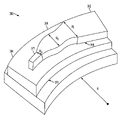
- FIG. 2 a gain chip 202 has been attached (e.g., soldered) to a submount 204 which acts as a heat sink for the gain chip 202 .
- Electrical connections to the gain chip 202 can be provided by bond wires or other means, which connections are not shown in FIG. 2 .
- the semiconductor optical waveguide 206 has both a curved portion 208 and a straight portion 210 .
- R radius of curvature
- L 1 is the length of the curved portion 208
- ⁇ is the angle at which the curved portion 208 intersects the front facet 212 relative to a normal axis 214 associated with the front facet 212 .
- Other curving functions e.g., sinusoidal or exponential, can be used to define the shape of the curved portion 208 .
- the total chip length L is the sum of L 1 and L 2 where L 2 is the length of the straight waveguide 210 .
- L 2 is the length of the straight waveguide 210 .
- exemplary embodiments of the present invention also provide a mode transformer in tandem with the curved waveguide structure.
- a mode transformer in tandem with the curved waveguide structure.
- such devices can be fabricated in different ways depending upon the desired characteristics, e.g., length, of the resulting gain chip 202 .
- one or both of the location and type of mode transformer which is employed can vary based on, among other things, the length of the gain chip 202 .
- a first exemplary embodiment as depicted generically by block 216 in FIG.
- a mode transformer 216 can be disposed within the gain chip 202 so as to be connected to, or form all or part of, the curved portion 208 of waveguide 206 .
- mode transformers per se, e.g., as described in U.S. Pat. Nos. 5,278,926 and 5,659,646, the disclosures of which are expressly incorporated here by reference, which techniques can be used to fabricate mode transformer 216 as all or part of the curved portion 208 of waveguide 206 .
- Applicants have recognized that by introducing curvature to the mode transformer 216 , the active regions thereof will experience greater losses than would be the case when employed in a mode transformer associated with a linear geometry. To minimize the losses associated with introducing curvature to the active regions of the mode transformer, Applicants have found that the use of a resonantly coupled mode transformer with a tapered active waveguide may be preferred for use as curved mode transformer 216 relative to other mode transformer implementations.
- a resonantly coupled mode transformer with a tapered active waveguide that can be adapted to function as all (or a portion of) the curved portion 208 of waveguide 206 can be found in U.S. Pat. No. 6,310,995, the disclosure of which is incorporated here by reference.
- This device can be adapted for use in a semiconductor package according to the present invention by applying the radius of curvature R to each of the surfaces of the device as shown in FIG. 3 .
- a resonant coupler 360 is shown coupling an active gain section 362 , a passive section 364 and an intermediate mode transformer section 366 .
- the coupler 360 resonantly couples modes bidirectionally between an active waveguide 368 and a passive waveguide 370 .
- the active gain section 362 can have a ridge width of approximately 2.5 ⁇ m, while the top waveguide 371 in the passive section can have a ridge width of about 0.3 ⁇ m
- the intermediate mode transformer 366 can have a length of about 100 ⁇ m
- the lengths and widths associated with the tapered mode transformer section 366 i.e., W P , W C , and W i , are selected to optimize coupling between the modes present in the active waveguide 368 and passive waveguide 370 , i.e., to create a taper that results in a phase matching condition occurring within the coupling length of the tapered region.
- the resulting optical mode is asymmetrical in the transverse cross-sectional plane as compared with other mode transformers wherein the optical mode is typically symmetrical.
- these types of mode transformers have the useful characteristic of being able to transform the mode of the optical energy from a more elliptical mode to a more circular mode using a curved geometry because the active region 362 of these devices is generally shorter than that found in other types of adiabatic mode transformers, thereby reducing the losses associated with introducing the curvature R.
- the mode transformer 216 can be disposed along the straight portion of the waveguide 206 as opposed to the curved portion 208 .
- the active region of the mode transformer 216 can be fabricated with a linear geometry to avoid the losses introduced by curvature.
- the curved portion 208 will then, in this exemplary embodiment, be a passive waveguide that is designed to support both a circular beam and the smaller radius of curvature R that is associated with the shorter gain chip 202 .
- a passive waveguide a more strongly confined mode can be supported in comparison with the active waveguide, leading to lower losses in the curved section of the waveguide and, consequently, to lower overall optical loss on the chip.
- the mode transformer 216 possesses a straight, or substantially straight, geometry in this exemplary embodiment, the selection of the type of mode transformer used in this embodiment need not be based on its ability to mitigate losses in the active region associated with curvature.
- any of the aforedescribed mode transformers, and other types, maybe employed as mode transformer 216 in the exemplary embodiment of FIG. 4 as long as they are consistent with the short chip length
- the mode tranformer 216 may or may not abut the curved portion 208 of the waveguide 206 .
- the choice of whether to implement the mode transformer 216 along the curved portion 208 or the straight portion 210 of the waveguide 206 will vary depending upon the desired gain chip implementation.
- One consideration in making this choice is that, for the same gain chip length, the length of the active region 210 of the waveguide 206 is shorter in the exemplary embodiment of FIG. 4 as compared with the exemplary embodiment of FIG. 2 due to the longer passive section 208 , 220 in the former emdodiment. In some applications it may be desirable to maximize the length of the active region, making the embodiment of FIG. 2 more desirable.
- another consideration is the chip length and corresponding radius of curvature of the curved portion of the waveguide.
- the mode transformer 216 may be implemented along the curved portion 208 of the waveguide 206 if the chip length is greater than, for example, 400 microns.
- the gain chip arrangement of FIG. 4 also confers manufacturing flexibility.
- the exemplary portion 600 of a semiconductor wafer shown in FIG. 6 Therein, devices are created in reverse orientation relative to one another on the semiconductor wafer, i.e., the curved portions 208 of the waveguides are disposed on opposite sides of the wafer surface.
- the mode transformers 216 , curved passive portions 208 , straight passive portions 220 and straight active portion 210 of the waveguide as illustrated in FIG. 6 , the device manufacturer can create different types of devices from the same semiconductor wafer by selecting which line or lines along which to cleave the wafer.
- the structure 600 is cleaved along lines A, C and E, then two of the single angled facet gain chips described above with respect to FIG. 4 will be created.
- one semiconductor optical amplifier (SOA) chip is created.
- SOA semiconductor optical amplifier
- Yet another option is to cleave along lines B, C and D to create two semiconductor laser chips, each having one mode transformer.
- cleaving along lines B and E will result in one SAF device having two mode transformers.
- This flexibility in device selection from the same structure created on a semiconductor wafer will enable devices according to the present invention to be manufactured more cost effectively.
- one skilled in the art may elect to fabricate SAF devices with the embodiment of FIG. 4 that are much longer than 500 um, e.g., up to or exceeding 1500 microns, to take advantage of this manufacturing flexibility.
Landscapes
- Physics & Mathematics (AREA)
- General Physics & Mathematics (AREA)
- Optics & Photonics (AREA)
- Engineering & Computer Science (AREA)
- Microelectronics & Electronic Packaging (AREA)
- Condensed Matter Physics & Semiconductors (AREA)
- Electromagnetism (AREA)
- Power Engineering (AREA)
- Semiconductor Lasers (AREA)
Abstract
Description
Claims (21)
Priority Applications (1)
| Application Number | Priority Date | Filing Date | Title |
|---|---|---|---|
| US10/270,370 US7190852B2 (en) | 2002-10-15 | 2002-10-15 | Semiconductor devices with curved waveguides and mode transformers |
Applications Claiming Priority (1)
| Application Number | Priority Date | Filing Date | Title |
|---|---|---|---|
| US10/270,370 US7190852B2 (en) | 2002-10-15 | 2002-10-15 | Semiconductor devices with curved waveguides and mode transformers |
Publications (2)
| Publication Number | Publication Date |
|---|---|
| US20040071384A1 US20040071384A1 (en) | 2004-04-15 |
| US7190852B2 true US7190852B2 (en) | 2007-03-13 |
Family
ID=32068959
Family Applications (1)
| Application Number | Title | Priority Date | Filing Date |
|---|---|---|---|
| US10/270,370 Expired - Lifetime US7190852B2 (en) | 2002-10-15 | 2002-10-15 | Semiconductor devices with curved waveguides and mode transformers |
Country Status (1)
| Country | Link |
|---|---|
| US (1) | US7190852B2 (en) |
Cited By (5)
| Publication number | Priority date | Publication date | Assignee | Title |
|---|---|---|---|---|
| US20090154935A1 (en) * | 2007-12-18 | 2009-06-18 | Shrenik Deliwala | Bidirectional optical link over a single multimode fiber or waveguide |
| US20110170825A1 (en) * | 2009-08-14 | 2011-07-14 | Massachusetts Institute Of Technology | Waveguide Coupler Having Continuous Three-Dimensional Tapering |
| US20120281274A1 (en) * | 2011-05-04 | 2012-11-08 | Electronics And Telecommunications Research Institute | Semiconductor optical devices and methods of fabricating the same |
| US20150036975A1 (en) * | 2013-07-30 | 2015-02-05 | President And Fellows Of Harvard College | Device support structures from bulk substrates |
| US9939582B2 (en) * | 2011-04-21 | 2018-04-10 | Lionix International Bv | Layer having a non-linear taper and method of fabrication |
Families Citing this family (9)
| Publication number | Priority date | Publication date | Assignee | Title |
|---|---|---|---|---|
| US20040057253A1 (en) * | 2002-09-25 | 2004-03-25 | International Business Machines Corporation | Optical backplane connector with positive feedback and mode conversion |
| JP2006086228A (en) * | 2004-09-14 | 2006-03-30 | Hamamatsu Photonics Kk | Array for semiconductor laser element |
| JP2010219227A (en) * | 2009-03-16 | 2010-09-30 | Nec Corp | Wavelength variable laser, and method of manufacturing the same |
| JP2011180180A (en) * | 2010-02-26 | 2011-09-15 | Sumitomo Bakelite Co Ltd | Optical waveguide, optical wiring, optoelectric hybrid substrate, and electronic equipment |
| US9606293B2 (en) | 2015-06-29 | 2017-03-28 | Elenion Technologies, Llc | Bent taper with varying widths for an optical waveguide |
| US9829632B2 (en) | 2015-06-29 | 2017-11-28 | Elenion Technologies, Llc | Bent and tapered optical waveguide for mode converter and polarization rotator |
| WO2021117161A1 (en) * | 2019-12-11 | 2021-06-17 | 日本電信電話株式会社 | Optical waveguide |
| CN113376742B (en) * | 2021-06-18 | 2022-09-13 | 哈尔滨理工大学 | Parameter selection method of simple high-conversion-rate conical mode converter |
| JP2023032196A (en) * | 2021-08-26 | 2023-03-09 | 日本電信電話株式会社 | Optical mode converter and optical mode multiplexer/demultiplexer |
Citations (15)
| Publication number | Priority date | Publication date | Assignee | Title |
|---|---|---|---|---|
| US5278926A (en) | 1991-12-04 | 1994-01-11 | Alcatel Alsthom Compagnie Generale | Widened output mode semiconductor optical component and method of fabricating it |
| US5659646A (en) | 1994-01-27 | 1997-08-19 | Alcatel N.V. | Optical waveguide transition and method of fabricating it |
| US5978400A (en) | 1995-03-07 | 1999-11-02 | British Telecommunications Public Limited Company | Laser |
| US5982531A (en) | 1996-03-05 | 1999-11-09 | Alcatel Optronics | Semiconductor optical amplifier |
| US6118803A (en) | 1997-11-21 | 2000-09-12 | Sdl, Inc. | Optically amplifying semiconductor diodes with curved waveguides for external cavities |
| US6310995B1 (en) | 1998-11-25 | 2001-10-30 | University Of Maryland | Resonantly coupled waveguides using a taper |
| US6314117B1 (en) | 1998-12-16 | 2001-11-06 | Quan Photonics, Inc | Laser diode package |
| US6411763B1 (en) * | 1998-09-24 | 2002-06-25 | Alcatel | Integrated optical component |
| US6456429B1 (en) | 2000-11-15 | 2002-09-24 | Onetta, Inc. | Double-pass optical amplifier |
| US6600847B2 (en) * | 2001-11-05 | 2003-07-29 | Quantum Photonics, Inc | Semiconductor optical device with improved efficiency and output beam characteristics |
| US20040126063A1 (en) * | 2000-02-25 | 2004-07-01 | Alphonse Gerard A | Multi-pass, arcuate bent waveguide, high power super luminescent diode |
| US6813404B2 (en) * | 2001-03-19 | 2004-11-02 | Nec Corporation | Integrated optical module |
| US6819814B2 (en) * | 1998-06-24 | 2004-11-16 | The Trustees Of Princeton University | Twin waveguide based design for photonic integrated circuits |
| US6856709B2 (en) * | 2001-11-01 | 2005-02-15 | Opnext Japan, Inc. | Optical modulation device |
| US20050175045A1 (en) * | 2002-02-28 | 2005-08-11 | Barbara Paldus | Laser tuning by spectrally dependent spatial filtering |
-
2002
- 2002-10-15 US US10/270,370 patent/US7190852B2/en not_active Expired - Lifetime
Patent Citations (15)
| Publication number | Priority date | Publication date | Assignee | Title |
|---|---|---|---|---|
| US5278926A (en) | 1991-12-04 | 1994-01-11 | Alcatel Alsthom Compagnie Generale | Widened output mode semiconductor optical component and method of fabricating it |
| US5659646A (en) | 1994-01-27 | 1997-08-19 | Alcatel N.V. | Optical waveguide transition and method of fabricating it |
| US5978400A (en) | 1995-03-07 | 1999-11-02 | British Telecommunications Public Limited Company | Laser |
| US5982531A (en) | 1996-03-05 | 1999-11-09 | Alcatel Optronics | Semiconductor optical amplifier |
| US6118803A (en) | 1997-11-21 | 2000-09-12 | Sdl, Inc. | Optically amplifying semiconductor diodes with curved waveguides for external cavities |
| US6819814B2 (en) * | 1998-06-24 | 2004-11-16 | The Trustees Of Princeton University | Twin waveguide based design for photonic integrated circuits |
| US6411763B1 (en) * | 1998-09-24 | 2002-06-25 | Alcatel | Integrated optical component |
| US6310995B1 (en) | 1998-11-25 | 2001-10-30 | University Of Maryland | Resonantly coupled waveguides using a taper |
| US6314117B1 (en) | 1998-12-16 | 2001-11-06 | Quan Photonics, Inc | Laser diode package |
| US20040126063A1 (en) * | 2000-02-25 | 2004-07-01 | Alphonse Gerard A | Multi-pass, arcuate bent waveguide, high power super luminescent diode |
| US6456429B1 (en) | 2000-11-15 | 2002-09-24 | Onetta, Inc. | Double-pass optical amplifier |
| US6813404B2 (en) * | 2001-03-19 | 2004-11-02 | Nec Corporation | Integrated optical module |
| US6856709B2 (en) * | 2001-11-01 | 2005-02-15 | Opnext Japan, Inc. | Optical modulation device |
| US6600847B2 (en) * | 2001-11-05 | 2003-07-29 | Quantum Photonics, Inc | Semiconductor optical device with improved efficiency and output beam characteristics |
| US20050175045A1 (en) * | 2002-02-28 | 2005-08-11 | Barbara Paldus | Laser tuning by spectrally dependent spatial filtering |
Non-Patent Citations (3)
| Title |
|---|
| Heim, Peter J.S. et al, "Single-Angled Facet Laser Diode for Tunable External Cavity Lasers", IEEE Princeton Section Sarnoff Symposium, Apr. 28, 1995. |
| Heim, Peter J.S. et al, "Single-Angled-Facet Laser Diode For Widely Tunable External Cavity Semiconductor Lasers with High Spectral Purity", Electronics Letters, vol. 33, No. 16, pp. 1387-1389, Jul. 1997. |
| Semenov, A.T. "Wide Spectrum Single Quantum Well Superluminescent Diodes at 0.8micrometers With Bent Optical Waveguide", Electronics Letters, vol. 29, No. 10, pp. 854-856, May 1993. |
Cited By (11)
| Publication number | Priority date | Publication date | Assignee | Title |
|---|---|---|---|---|
| US20090154935A1 (en) * | 2007-12-18 | 2009-06-18 | Shrenik Deliwala | Bidirectional optical link over a single multimode fiber or waveguide |
| US7693373B2 (en) * | 2007-12-18 | 2010-04-06 | Analog Devices, Inc. | Bidirectional optical link over a single multimode fiber or waveguide |
| US20100284699A1 (en) * | 2007-12-18 | 2010-11-11 | Analog Devices, Inc. | Bidirectional optical link over a single multimode fiber or waveguide |
| US8542965B2 (en) * | 2007-12-18 | 2013-09-24 | Analog Devices, Inc. | Bidirectional optical link over a single multimode fiber or waveguide |
| US20110170825A1 (en) * | 2009-08-14 | 2011-07-14 | Massachusetts Institute Of Technology | Waveguide Coupler Having Continuous Three-Dimensional Tapering |
| US8472766B2 (en) * | 2009-08-14 | 2013-06-25 | Massachusetts Institute Of Technology | Waveguide coupler having continuous three-dimensional tapering |
| US9939582B2 (en) * | 2011-04-21 | 2018-04-10 | Lionix International Bv | Layer having a non-linear taper and method of fabrication |
| US20120281274A1 (en) * | 2011-05-04 | 2012-11-08 | Electronics And Telecommunications Research Institute | Semiconductor optical devices and methods of fabricating the same |
| US8804232B2 (en) * | 2011-05-04 | 2014-08-12 | Electronics And Telecommunications Research Institute | Semiconductor optical devices and methods of fabricating the same |
| US20150036975A1 (en) * | 2013-07-30 | 2015-02-05 | President And Fellows Of Harvard College | Device support structures from bulk substrates |
| US10281648B2 (en) * | 2013-07-30 | 2019-05-07 | President And Fellows Of Harvard College | Device support structures from bulk substrates |
Also Published As
| Publication number | Publication date |
|---|---|
| US20040071384A1 (en) | 2004-04-15 |
Similar Documents
| Publication | Publication Date | Title |
|---|---|---|
| JP5082414B2 (en) | Optical semiconductor device and optical waveguide device | |
| US6580850B1 (en) | Optical waveguide multimode to single mode transformer | |
| US10608410B2 (en) | Single facet laser sources | |
| EP1210753B1 (en) | Tunable laser source with integrated optical amplifier | |
| US6091755A (en) | Optically amplifying semiconductor diodes with curved waveguides for external cavities | |
| US11728622B2 (en) | Single-facet, variable-confinement optical waveguide amplifier | |
| US7190852B2 (en) | Semiconductor devices with curved waveguides and mode transformers | |
| CN103875140B (en) | There is the high-power semiconductor laser of phase-matched optical element | |
| JP4827410B2 (en) | High power semiconductor laser diode and method of manufacturing such a diode | |
| US20020154393A1 (en) | Semiconductor optical amplifier and semiconductor laser | |
| WO2001017076A2 (en) | Tunable laser source with integrated optical amplifier | |
| CN112868149A (en) | Optical amplifier | |
| US20060034576A1 (en) | Superluminescent diodes having high output power and reduced internal reflections | |
| JPH11511911A (en) | Opto-semiconductor component with deep ridge waveguide | |
| US6499888B1 (en) | Wide ridge pump laser | |
| US6658035B1 (en) | Tunable laser source with integrated optical amplifier | |
| US20230296841A1 (en) | Optical component | |
| US7215686B2 (en) | Waveguide structure having improved reflective mirror features | |
| US6574262B1 (en) | High-power and high efficiency large area single-mode laser | |
| WO2002029905A1 (en) | Optical mode size converter | |
| US6711199B2 (en) | Laser diode with an internal mirror | |
| US20250329993A1 (en) | Semiconductor optical amplifier | |
| JP3411324B2 (en) | Semiconductor laser with waveguide | |
| JP2003518758A (en) | Pump laser with wide ridge | |
| US6829276B1 (en) | Integrated high power semiconductor laser |
Legal Events
| Date | Code | Title | Description |
|---|---|---|---|
| AS | Assignment |
Owner name: QUANTUM PHOTONICS, INC., MARYLAND Free format text: ASSIGNMENT OF ASSIGNORS INTEREST;ASSIGNORS:HEIM, PETER J.S.;DAGENAIS, MARIO;SAINI, SIMARJEET S.;REEL/FRAME:013647/0507 Effective date: 20021018 |
|
| AS | Assignment |
Owner name: COMERICA BANK, CALIFORNIA Free format text: INTELLECTUAL PROPERTY SECURITY AGREEMENT;ASSIGNOR:COVEGA CORPORATION;REEL/FRAME:015766/0083 Effective date: 20050210 |
|
| AS | Assignment |
Owner name: COVEGA CORPORATION, MARYLAND Free format text: CHANGE OF NAME;ASSIGNOR:QUANTUM PHOTONICS, INC.;REEL/FRAME:018591/0812 Effective date: 20030311 |
|
| STCF | Information on status: patent grant |
Free format text: PATENTED CASE |
|
| AS | Assignment |
Owner name: SQUARE 1 BANK, NORTH CAROLINA Free format text: ASSIGNMENT OF ASSIGNORS INTEREST;ASSIGNOR:COVEGA CORPORATION;REEL/FRAME:019265/0490 Effective date: 20060807 |
|
| FEPP | Fee payment procedure |
Free format text: PAYOR NUMBER ASSIGNED (ORIGINAL EVENT CODE: ASPN); ENTITY STATUS OF PATENT OWNER: LARGE ENTITY |
|
| AS | Assignment |
Owner name: COVEGA CORPORATION, MARYLAND Free format text: RELEASE BY SECURED PARTY;ASSIGNOR:SQUARE BANK 1;REEL/FRAME:022408/0516 Effective date: 20090317 |
|
| AS | Assignment |
Owner name: COVEGA CORPORATION, NEW JERSEY Free format text: RELEASE BY SECURED PARTY;ASSIGNOR:COMERICA BANK;REEL/FRAME:022416/0253 Effective date: 20090317 |
|
| AS | Assignment |
Owner name: THORLABS QUANTUM ELECTRONICS, INC., NEW JERSEY Free format text: ASSIGNMENT OF ASSIGNORS INTEREST;ASSIGNOR:COVEGA CORPORATION;REEL/FRAME:022427/0994 Effective date: 20090317 |
|
| FEPP | Fee payment procedure |
Free format text: PAT HOLDER NO LONGER CLAIMS SMALL ENTITY STATUS, ENTITY STATUS SET TO UNDISCOUNTED (ORIGINAL EVENT CODE: STOL); ENTITY STATUS OF PATENT OWNER: LARGE ENTITY |
|
| FPAY | Fee payment |
Year of fee payment: 4 |
|
| FPAY | Fee payment |
Year of fee payment: 8 |
|
| MAFP | Maintenance fee payment |
Free format text: PAYMENT OF MAINTENANCE FEE, 12TH YEAR, LARGE ENTITY (ORIGINAL EVENT CODE: M1553); ENTITY STATUS OF PATENT OWNER: LARGE ENTITY Year of fee payment: 12 |