US7190850B2 - PMD emulator - Google Patents
PMD emulator Download PDFInfo
- Publication number
- US7190850B2 US7190850B2 US11/087,532 US8753205A US7190850B2 US 7190850 B2 US7190850 B2 US 7190850B2 US 8753205 A US8753205 A US 8753205A US 7190850 B2 US7190850 B2 US 7190850B2
- Authority
- US
- United States
- Prior art keywords
- dgd
- polarization
- pmd
- sections
- emulator
- Prior art date
- Legal status (The legal status is an assumption and is not a legal conclusion. Google has not performed a legal analysis and makes no representation as to the accuracy of the status listed.)
- Expired - Fee Related
Links
Images


Classifications
-
- G—PHYSICS
- G02—OPTICS
- G02F—OPTICAL DEVICES OR ARRANGEMENTS FOR THE CONTROL OF LIGHT BY MODIFICATION OF THE OPTICAL PROPERTIES OF THE MEDIA OF THE ELEMENTS INVOLVED THEREIN; NON-LINEAR OPTICS; FREQUENCY-CHANGING OF LIGHT; OPTICAL LOGIC ELEMENTS; OPTICAL ANALOGUE/DIGITAL CONVERTERS
- G02F1/00—Devices or arrangements for the control of the intensity, colour, phase, polarisation or direction of light arriving from an independent light source, e.g. switching, gating or modulating; Non-linear optics
- G02F1/01—Devices or arrangements for the control of the intensity, colour, phase, polarisation or direction of light arriving from an independent light source, e.g. switching, gating or modulating; Non-linear optics for the control of the intensity, phase, polarisation or colour
- G02F1/0136—Devices or arrangements for the control of the intensity, colour, phase, polarisation or direction of light arriving from an independent light source, e.g. switching, gating or modulating; Non-linear optics for the control of the intensity, phase, polarisation or colour for the control of polarisation, e.g. state of polarisation [SOP] control, polarisation scrambling, TE-TM mode conversion or separation
-
- H—ELECTRICITY
- H04—ELECTRIC COMMUNICATION TECHNIQUE
- H04B—TRANSMISSION
- H04B10/00—Transmission systems employing electromagnetic waves other than radio-waves, e.g. infrared, visible or ultraviolet light, or employing corpuscular radiation, e.g. quantum communication
- H04B10/25—Arrangements specific to fibre transmission
- H04B10/2507—Arrangements specific to fibre transmission for the reduction or elimination of distortion or dispersion
- H04B10/2569—Arrangements specific to fibre transmission for the reduction or elimination of distortion or dispersion due to polarisation mode dispersion [PMD]
-
- G—PHYSICS
- G02—OPTICS
- G02F—OPTICAL DEVICES OR ARRANGEMENTS FOR THE CONTROL OF LIGHT BY MODIFICATION OF THE OPTICAL PROPERTIES OF THE MEDIA OF THE ELEMENTS INVOLVED THEREIN; NON-LINEAR OPTICS; FREQUENCY-CHANGING OF LIGHT; OPTICAL LOGIC ELEMENTS; OPTICAL ANALOGUE/DIGITAL CONVERTERS
- G02F1/00—Devices or arrangements for the control of the intensity, colour, phase, polarisation or direction of light arriving from an independent light source, e.g. switching, gating or modulating; Non-linear optics
- G02F1/01—Devices or arrangements for the control of the intensity, colour, phase, polarisation or direction of light arriving from an independent light source, e.g. switching, gating or modulating; Non-linear optics for the control of the intensity, phase, polarisation or colour
- G02F1/09—Devices or arrangements for the control of the intensity, colour, phase, polarisation or direction of light arriving from an independent light source, e.g. switching, gating or modulating; Non-linear optics for the control of the intensity, phase, polarisation or colour based on magneto-optical elements, e.g. exhibiting Faraday effect
-
- G—PHYSICS
- G02—OPTICS
- G02F—OPTICAL DEVICES OR ARRANGEMENTS FOR THE CONTROL OF LIGHT BY MODIFICATION OF THE OPTICAL PROPERTIES OF THE MEDIA OF THE ELEMENTS INVOLVED THEREIN; NON-LINEAR OPTICS; FREQUENCY-CHANGING OF LIGHT; OPTICAL LOGIC ELEMENTS; OPTICAL ANALOGUE/DIGITAL CONVERTERS
- G02F2201/00—Constructional arrangements not provided for in groups G02F1/00 - G02F7/00
- G02F2201/16—Constructional arrangements not provided for in groups G02F1/00 - G02F7/00 series; tandem
-
- G—PHYSICS
- G02—OPTICS
- G02F—OPTICAL DEVICES OR ARRANGEMENTS FOR THE CONTROL OF LIGHT BY MODIFICATION OF THE OPTICAL PROPERTIES OF THE MEDIA OF THE ELEMENTS INVOLVED THEREIN; NON-LINEAR OPTICS; FREQUENCY-CHANGING OF LIGHT; OPTICAL LOGIC ELEMENTS; OPTICAL ANALOGUE/DIGITAL CONVERTERS
- G02F2202/00—Materials and properties
- G02F2202/20—LiNbO3, LiTaO3
Definitions
- the present invention relates to a PMD (Polarization Mode Dispersion) emulator for estimating PMD which occurs when signal light propagates or for compensating optical transmission path.
- PMD Polarization Mode Dispersion
- WDM Widelength Division Multiplexing
- PMD Polarization Mode Dispersion
- PMD of an optical fiber installed in previous years is around 1 ps/km 1/2 and therefore, when the bit rate is 10 Gb/s, possible transmission distance is about 170 km while when the bit rate is 40 Gb/s, possible transmission distance is decreased to be only 10 km.
- PMD affects optical transmission significantly, which results in difficulty to construct a high-bit-rate practical optical transmission system.
- a PMD emulator is used to estimate a PMD characteristic in an optical transmission system which performs transmission at a high bit rate, and to compensate PMD which occurs in the optical transmission system.
- a conventional PMD emulator used to emulate PMD characteristics of an actually used SMF (Single Mode Fiber) is described. If PMD is estimated with use of an actual SMF in an experimental laboratory, as the experimental laboratory is an environment more stable than the place where the SMF is actually installed, more time will be required. Accordingly, it is effective to use a PMD emulator to perform PMD estimation.
- An SMF used in this example is tens through hundreds of kilometer long and PMD is zero through tens ps approximately and two or more PMD are included.
- first-order PMD DMD: Differential Group Delay
- SOPMD second-order PMD
- FIG. 18 A schematic view of the PMD emulator of this example is shown in FIG. 18 .
- This PMD emulator is modeled by coupling plural (for example 100) DGD sections 161 1 through 161 n .
- a birefringent portion is used in a DGD section.
- DGD sections 161 1 through 161 n are rotated.
- the rotation speed is different between DGD sections however, each rotation speed is fixed and the speed is not controlled.
- FIG. 19 is a graph showing DGD and SOPMD characteristics obtained by this PMS emulator.
- the horizontal axis of the graph indicates a wavelength (nm) and the vertical axis indicates DGD (ps) and SOPMD (ps 2 ).
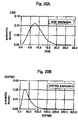
- FIG. 20A shows DGD distribution and FIG. 20B shows SOPMD distribution. Correlation between DGD and SOPMD at each wavelength is proved to be positive as shown in FIG. 21 .
- FIG. 17 shows a schematic configuration of this device. Light to be measured is input into this device and then an accurate PMD can be obtained.
- This PMD emulator 100 includes an input-side optical fiber 101 and an output-side optical fiber 102 , birefringent portions 104 , 106 and 108 which are composed of DGD portions 122 , 132 and 142 and phase shift portions 124 , 134 and 144 , respectively and polarization mode mixing portions 110 , 112 and 114 .
- the birefringent portions 104 , 106 and 108 and polarization mode mixing portions 110 , 112 and 114 are connected by turn to make up plural stages (one birefringent portion and one polarization mode mixing portion consist in one stage). In FIG. 17 , N stages made up of N birefringent portions and N polarization mode mixing portions are shown.
- phase shift portions 124 , 134 and 144 are provided with controllers 126 , 136 and 146 for controlling a phase shift amount while the polarization mode mixing portions are provided with controllers 116 , 118 and 120 for controlling polarization rotational direction.
- PMD generated in a transmission path installed previously is distributed in the temporal direction and in the frequency direction. These distributions are in accordance with theoretically shown probability density distribution, DGD (first-order PMD) is given a Maxwell's distribution and SOPMD (second-order PMD) is given a corresponding probability density function (see OPTICAL FIBER TELECOMMUNICATIONS, VOLUME IVB, Chapter 5 “Polarization-Mode Dispersion”).
- PMD emulator configured of multi-stage DGD sections of polarization maintaining fiber or a birefringent crystal, a variable polarization rotator being arranged between every two of the DGD sections and rotates them at randomly set rotation angle (see Proc.PFC02, paper ThA3, pp 374–375, 2002).
- YVO4 or LiNbO3 used as a polarization mode mixing portion is YVO4 or LiNbO3. Since they utilize electro-optic effect, a large-scale device such as a piezoelectric element is required, which presents a problem of large power consumption. YVO4 and LiNbO3 also present a problem of large insertion loss.
- An object of the present invention is to provide a PMD emulator which operates stably at low power consumption, which is low in insertion loss, which is configured of less components, which does not need a complex and expensive device, which generate a desired DGD value at some time, which allows an average DGD to be changed without changing DGD values of respective sections and which can obtain PMD characteristics without changing a connection angle.
- a PMD emulator of the present invention is a PMD emulator comprising:
- an input-side optical fiber for receiving light to be measured
- an output-side optical fiber for outputting the light to be measured
- a first polarization rotating portion including M DGD sections (M is an integer equal to or more than 2) concatenated by (M ⁇ 1) polarization rotators, one DGD section being arranged at each end of said first polarization rotating portion;
- a second polarization rotating portion including N DGD sections (N is an integer equal to or more than 2) concatenated by (N ⁇ 1) polarization rotators, one DGD section being arranged at each end of said second polarization rotating portion; and
- said input-side optical fiber is connected to a DGD section at an input side of said first polarization rotating portion, a DGD section at an output side of said first polarization rotating portion being connected to a connecting portion at an input side of said arbitrary-arbitrary polarization controller, a connecting portion at an output side of said arbitrary-arbitrary polarization controller being connected to a DGD section at an input side of said second rotating portion, and a DGD section at an output side of said second polarization rotating portion being connected to said output-side optical fiber.
- PMD emulator of the present invention is a PMD emulator in which said polarization controller has a polarization shifter connected between polarization rotators.
- PMD emulator of the present invention is a PMD emulator in which M is 2 and N is 2.
- PMD emulator of the present invention is a PMD emulator in which said polarization rotators are controlled based on a control parameter obtained by a simulation thereby to generate a desired PMD value.
- PMD emulator of the present invention is a PMD emulator in which said polarization rotators are controlled to change an average DGD without changing DGD characteristics of the DGD sections.
- PMD emulator of the present invention is a PMD emulator including 40 or more DGD sections connected with a random relative angle and a temperature controlling mechanism for changing a temperature as a whole.
- PMD emulator of the present invention is a PMD emulator in which the DGD sections have difference DGD in accordance with normal distribution.
- PMD emulator of the present invention is a PMD emulator in which standard deviation of the normal distribution is 20% of an average of the normal distribution.
- PMD emulator of the present invention is a PMD emulator in which the DGD sections are polarization maintaining fibers or uniaxial birefringent crystals.
- FIGS. 1A and 1B are views each illustrating a configuration of a PMD emulator according to the present invention
- FIGS. 2A through 2C are graphs each for comparing PMD calculated values with measured values by a conventional PMD emulator consisting of 100 DGD sections;
- FIGS. 3A through 3C are graphs each for comparing PMD calculated values with measured values obtained after given rotation by a PMD emulator consisting of four DGD sections;
- FIGS. 4A through 4C are graphs each for comparing DGD calculated values with measured values by a PMD emulator consisting of four DGD sections according to the present invention
- FIG. 5 is a view illustrating another configuration of a PMD emulator according to the present invention.
- FIG. 6 is a view illustrating another configuration of the PMD emulator on FIG. 5 ;
- FIG. 7 is a view illustrating another configuration of the PMD emulator on FIG. 6 ;
- FIG. 8 is a view illustrating yet another configuration of the PMD emulator on FIG. 6 ;
- FIG. 9 is a view illustrating yet another configuration of the PMD emulator on FIG. 6 ;
- FIG. 10 is a view illustrating a configuration of a PMD measuring unit
- FIG. 11 is a graph of DGD values for comparing PMD characteristics of a PMD emulator and calculated values in theory
- FIG. 12 is a graph of SOPMD values for comparing PMD characteristics of a PMD emulator and calculated values in theory
- FIG. 13 is a graph of PCD absolute values and PSD divided from SOPMD values for comparing PMD characteristics of a PMD emulator and calculated values in theory
- FIG. 14 shows calculation results of DGD distribution
- FIG. 15 is a view illustrating a PMD emulator configured by connecting 40 or more DGD sections with relative angles determined in a random fashion;
- FIG. 16 shows calculation results of DGD distribution in a PMD emulator shown on FIG. 15 ;
- FIG. 17 is a view illustrating a configuration of a conventional PMD emulator
- FIG. 18 is a view illustrating a configuration of a conventional PMD emulator
- FIG. 19 is a graph showing DGD and SOPMD characteristics of a SMF
- FIG. 20A is a graph of DGD distribution
- FIG. 20B is a graph of SOPMD distribution
- FIG. 21 is a graph showing a relationship between DGD and SOPMD
- FIG. 22 is a view illustrating a configuration of a conventional PMD emulator
- FIG. 23 is a schematic view of a LN waveguide polarization controller according to the present invention.
- FIG. 24 is a schematic diagram showing a state of refractive index when an LN waveguide polarization controller is used as a mode converter
- FIG. 25 is a view for explaining a way of applying to upper and lower electrodes voltages of the same magnitude but different signs;
- FIG. 26 is a view for explaining a way of applying to upper and lower electrodes voltages of the same magnitude and sign;
- FIG. 27 is a view showing an electrolytic component applied effectively on a wave 6 guide, and an original state and a changed state of refractive indexes;
- FIG. 28 is a view showing an effect of the way of applying voltages of the same magnitude and sign to upper and lower electrodes
- FIG. 29 is a view showing a principle when an LN waveguide polarization controller is used as a waveplate.
- FIG. 30 is a view showing a state of refractive indexes when a waveplate is under operation.
- PMD Polarization Mode Dispersion
- PMFs polarization maintaining fibers
- ⁇ (n+1) The first-order PMD vector output by the (n+1)th DGD section, ⁇ (n+1), and the second-order PMD vector, ⁇ (n+1), are represented by connection relational equations as shown below:
- ⁇ n+1 is the first-order PMD vector output by the (n+1)th DGD section
- ⁇ (n) is the first-order PMD vector output by first n DGD sections
- Rn is rotation matrix for the n-th rotation polarizer
- the amount of PMD (DGD and SOPMD) generated by two DGD sections may be represented as:
- ⁇ 1 and ⁇ 2 are the DGD of the two DGD sections and ⁇ is the rotation angle.
- the DGD and the SOPMD are independent of frequency. The subfix denotes differentiation.
- ⁇ is the DGD
- ⁇ is angular frequency of the carrier wave.
- SOPMD since the SOPMD is always perpendicular to the first-order PMD vector, SOPMD has only the PSD component.
- the DGD and SOPMD generated by the concatenation of more than two DGD sections have a periodic characteristic with respect to frequency, and the SOPMD has two components.
- the free spectrum range (FSR) of a device is determined by the length of each DGD section.
- FSR free spectrum range
- a plurality of FSRs are mixed, however, if the plurality of FSRs are equal, a single FSR can be generated for whole the emulator, and stable emulator characteristic can be achieved.
- FSRs are shifted by the same amount, the characteristics can be shifted while keeping the characteristic profile.
- FIGS. 1A and 1B show an embodiment of a PMD emulator including a polarization controller according to the present invention.
- the first polarization rotating unit 73 is configured by connecting the DGD section 76 to a polarization rotator 80 , and connecting the polarization rotator 80 to the DGD section 77 .
- the second polarization rotating unit 74 is configured by connecting the DGD section 78 to a polarization rotator 81 , and connecting the polarization rotator 81 to the DGD section 79 .
- An input-side optical fiber 71 which receives light to be measured is connected to the DGD section 76 which is located at the input side of the first polarization rotating unit 73 .
- the DGD section 77 at the output side of the first polarization rotating unit 73 is connected to a connecting portion at the input side of an arbitrary-arbitrary polarization controller 75 .
- a connecting portion at the output side of the arbitrary-arbitrary polarization controller 75 is connected to the DGD section 78 at the input side of the second polarization rotating unit 74 .
- the DGD section 79 at the output side of the second polarization rotating unit 74 is connected to the output-side optical fiber 72 which outputs light to be measured.
- the DGD sections 76 through 79 are made of PMFs (Polarization Maintaining Fibers). However, they may be made of birefringent crystals such as TiO2 instead of PMF.
- the polarization rotators 80 and 81 may be realized by Faraday rotators or by rotating a 1 ⁇ 2 waveplate.
- FIG. 1B shows an arbitrary-arbitrary polarization controller 75 of the present embodiment.
- the arbitrary-arbitrary polarization controller 75 has the most common configuration such that a polarization rotator 83 and a polarization rotator 84 are connected to a polarization shifter 82 interposed therebetween.
- This configuration can be realized by a smaller number of components than another configuration and therefore can provide an inexpensive device.
- the polarization rotators 83 and 84 configured of the arbitrary-arbitrary polarization controller 75 may be realized by Faraday rotators or by rotating a 1 ⁇ 2 waveplate.
- the polarization shifter 82 may be realized by sandwiching a polarization rotator between two 1 ⁇ 4 waveplates.
- light to be measured transmitted on the input-side optical fiber 71 is propagated along the DGD section 76 , the polarization rotator 80 , the DGD section 77 , polarization rotator 83 , the polarization shifter 82 , the polarization rotator 84 , the DGD section 78 , the polarization rotator 81 and DGD section 79 , in this order, and is transmitted to the outside from the output-side optical fiber 72 .
- collimators are arranged at ends of input-side optical fiber 71 and the output-side optical fiber 72 .
- M and N may be set at any numbers more than 2.
- simulations are performed of a PMD emulator with a large number of DGD sections by computer calculation so as to obtain temporal change of DGD and SOPMD values (the PMD emulator is not activated in fact).
- non-linear fitting is performed by the same computer calculation to calculate a control parameter of each polarization rotator of the PMD emulator 70 corresponding to desired DGD and SOPMD values.
- This calculated control parameter can be utilized to activate the PMD emulator 70 with four DGD section so as to generate desired DGD and SOPMD values.
- the DGD and SOPMD values generated by the PMD emulator 70 can be measured by a polarization mode dispersion measuring unit.
- the average DGD can be changed by accurately controlling polarization rotators.
- FIG. 2A is a graph for comparing a DGD characteristic based on calculated values with measured values by a conventional PMD emulator consisting of 100 DGD sections. An average DGD of this PMD emulator is 10 ps.
- FIG. 2B is a graph for comparing a SOPMD characteristic based on calculated values with measured values by a conventional PMD emulator. As is seen from FIGS. 2A and 2B , for both of DGD and SOPMD, the calculated values almost agree with measured values.
- FIG. 2C is a graph for showing correlation between DGD measured values and SOPMD measured values, which shows they are in positive correlation.
- FIG. 3A is a graph comparing DGD calculated values with DGD measured values obtained after rotation at a given rotational speed (with no particular control) in a PMD emulator consisting of four DGD sections of 8 ps DGD according to the present invention.
- FIG. 3B is a graph comparing SOPMD calculated values with SOPMD measured values obtained after rotation at a given rotational speed in a PMD emulator 70 consisting of four DGD sections. As is seen from FIGS. 3A and 3B , for both of the DGD and SOPMD, the calculation and the measurement present different values.
- FIG. 3C is a graph for showing correlation between DGD measured values and SOPMD measured values. This graph shows that there is no correlation between them.
- FIG. 4A is a graph for comparing calculated DGD characteristic with measured DGD values obtained when a polarization rotator is accurately controlled in a PMD emulator according to the present invention, the PMD emulator being configured by four DGD sections each with 8 ps DGD.
- FIG. 4B is a graph for comparing calculated SOPMD characteristic with measured SOPMD characteristic obtained when a polarization rotator is accurately controlled in a PMD emulator with four DGD sections. For both of DGD and SOPMD, the calculated values and the measured values are almost identical.
- FIG. 4C is a graph for showing correlation between DGD measured values and the SOPMD measured values. This graph shows that they have positive correlation.
- FIG. 5 shows a configuration of another embodiment of the present invention.
- a PMD emulator 10 of this embodiment includes optical fibers 12 and 14 for inputting and outputting light to be measured, and four DGD sections 16 and three polarization controllers 18 , and four DGD sections 16 and three polarization controllers 18 are connected by turns.
- a polarization controller 18 consists of a Faraday rotator and a DGD section 16 consists of a PMF (Polarization Maintaining Fiber).
- the DGD section 16 may be made of a birefringent crystal such as TiO2 instead of PMF.
- first DGD section 16 a first polarization controller, a second DGD section 16 , a second polarization controller 18 , a third DGD section 16 and a third polarization controller and a fourth DGD section 16 in this order, and the fourth DGD section 16 is coupled to an output-side optical fiber 14 .
- first DGD section 16 and the fourth DGD section 16 are made of crystals, collimators (not shown) are arranged at ends of the optical fibers 12 and 14 .
- the four DGD sections 16 and the three polarization controllers 18 are connected by turns, however, the numbers of DGD sections and polarization controllers are not limited to such a configuration. For example, five, six, . . . N DGD sections 16 may be arranged. Since a polarization controller is arranged between DGD sections 16 , the number of polarization controllers to be arranged is one less than the number of DGD sections 16 . In other words, if the number of DGD sections 16 is N, the number of polarization controllers 18 to be arranged will be (N ⁇ 1).
- a Faraday rotator is used to control polarization rotation of light output from a DGD section 6 .
- the polarization controller 18 controls the angle of polarization surface of light in the reverse direction to traveling light. Since the Faraday rotator controls polarization rotation with a current of approximately 20 mA, it is characterized by low power consumption.
- FIG. 6 Another embodiment of a PMD emulator is described with reference to FIG. 6 .
- the PMD emulator 30 shown in FIG. 6 is configured differently from that in FIG. 5 in that a shifter 32 is arranged in the PMD emulator.
- DGD sections 16 and polarization controllers 18 are configured and arranged in the same fashion, however, a shifter 32 is connected to each of the polarization controllers 18 , which presents a difference in configuration between the PMD emulator of FIG. 6 from that of FIG. 5 .
- a shifter 32 is made of a Faraday rotator arranged between two 1 ⁇ 4 waveplates.
- shifters 32 are arranged. With the configuration on FIG. 6 , shifters 32 which are the same in number as the polarization controllers 18 will be arranged. Each of shifters 32 is arranged nearer to the input-side optical fiber 12 than the corresponding polarization controller 18 is.
- the number of shifters 32 may be set to (N ⁇ 2) depending on arrangement. An example of such a configuration is described with reference to FIG. 7 .
- FIG. 7 shows a configuration of a PMD emulator 40 which includes N DGD sections 16 , (N ⁇ 1) polarization controllers 18 and (N ⁇ 2) shifters 32 .
- an input-side optical fiber 12 , a first DGD section 16 , a first polarization controller 18 and a first shifter 32 are arranged in this order.
- a second DGD section 16 Arranged next to the first shifter 32 are a second DGD section 16 , a second polarization controller 18 and a second shifter 32 in this order.
- a third DGD section 16 Arranged next to the second shifter 32 are a third DGD section 16 , a third polarization controller 18 , a third shifter 32 , a fourth DGD section, . . . , a (n ⁇ 1)th DGD section 16 , a (n ⁇ 2)th polarization controller 18 and a (n ⁇ 2)th shifter 32 .
- n ⁇ 1)th DGD section 16 and a (n ⁇ 1)th polarization controller 18 are arranged at the (n ⁇ 1)th stage, and only a nth DGD section 16 is arranged at the nth stage.
- the nth DGD section 16 is then connected to the output-side optical fiber 14 .
- a configuration of a PMD emulator 50 shown in FIG. 8 may be adopted, in which a first DGD section 16 and a first polarization controller 18 are arranged in this order, and then, a second DGD section 16 , a first shifter 32 and a second polarization controller 18 are arranged in this order. These are followed by a third DGD section 16 , a second shifter 32 and a third polarization controller 18 arranged in this order. DGD sections 16 , shifters and polarization controllers are arranged in this way until the (n ⁇ 1)th polarization controller 18 , and after the (n ⁇ 1)th polarization controller 18 nth DGD section 16 is arranged.
- a configuration of a PMD emulator 60 shown in FIG. 9 may be adopted, in which a first shifter 32 is arranged between a second polarization controller 18 and a second DGD section 16 , and a second shifter 32 is arranged between the second polarization controller 18 and a third DGD section.
- shifters 32 are arranged to be connected one between an even-numbered polarization controller 18 and a DGD section 18 anterior to the polarization controller 18 and one between the polarization controller 18 and a DGD section 18 posterior to the polarization controller 18 .
- Polarization controllers 18 are three Faraday rotators which function as polarization rotator. Connected to the respective polarization controllers 18 are four DGD sections 16 , which is composed of PMFs.
- DGD sections 16 Although the number of DGD sections 16 is four, that number can be reduced by setting VFR angles to zero. For example, setting any two angles to zero reduces the number of DGD sections to two.
- This PMD measuring unit 50 is based on the general polarization analysis method, and a polarizer 581 and a Faraday rotator 58 b which functions as a polarization rotator are used as a polarization controller 58 .
- a PMD vector is analyzed by the Muller matrix method (MMM), and is determined by measuring the two output Stokes vectors resulting from two orthogonal input Stokes vectors. Two Stokes vector measurements performed at different wavelengths are required to determine the PMD vector at one wavelength. Determining SOPMD requires Stokes vector measurement at one more wavelength. Determining SOPMD requires the measurement of at least two Stokes responses at three wavelengths. For accurate determination, these measurements have to be completed before the PMD, the SOPMD and the polarization states of the DUT change.
- MMMM Muller matrix method
- a polarization controller (Faraday rotator) that has a short response time for input SOP control
- measurement time can be shortened and precise measurement of PMD vector becomes possible.
- precise measurement of the two components of SOPMD can be performed.
- the response time of the Faraday rotator for a ⁇ /2 rotation is less than 0.2 ms.
- FIGS. 11 and 12 show DGD and SOPMD characteristics by PMD emulator and theoretical calculated values
- FIG. 11 shows DGD
- FIG. 12 shows SOPMD.
- the data generated by PMD emulator proved to be repeatable and the sets of values are consistent.
- FIG. 13 shows the absolute values of PCD and PSD separated from SOPMD when the target SOPMD was set to 100 ps 2 , demonstrating good agreement between the measured and theoretical values. Because PCD is zero at the center frequency, SOPMD includes only the PSD component at that frequency. The ratio of PCD to PSD increases as the frequency deviates from the center frequency and the PSD component is shown again at the half cycle.
- the two-section configuration of the emulator can generate flat PMD spectrum in frequency. Then, target SOPMD can be set to 75, 100 and 125 ps2. This PMD emulator can generate more than 2 kinds of PMD with SOPMD fixed. With use of this PMD emulator, it is possible to estimate degradation in performance by two components of SOPMD in an optical communication system.
- a programmable PMD emulator which uses a polarization controller (Faraday rotator) and a PMD measuring unit enable accurate calculation.
- this PMD emulator is stable and DGD and two components of SOPMD obtained by measuring by the PMD measuring unit PMD generated by the PMD emulator are in good agreement with theoretical calculation values.
- ⁇ i( ⁇ ) denotes the phase of a component in defiance of fluctuation of DGD sections and depends on a frequency
- ⁇ i( ⁇ , t) denotes the phase of a component which fluctuates depending on the ambient temperature and depends on a frequency and the ambient temperature.
- variable parameters in this model are a rotation angle ⁇ i and a phase ⁇ i( ⁇ ,t) by fluctuation.
- FIGS. 2A through 2 c show calculation results of DGD (first-order PMD) distribution obtained when in the above model, the number of stages of DGD sections is changed and ⁇ i(t) is only a random number, ((t) is fixed to be a random number), (t) is only a random number ( ⁇ i(t) is fixed to be a random number) and both are set to random numbers.
- a value of DGD section is determined so as to have an average DGD of 30 ps.
- normal distribution of each DGD section is given so that standard deviation can be 20% of the average.
- Total DGD is a sum of DGD values of used DGD sections and “average DGD” denotes an average value of used DGD sections.
- the resultant distribution is close to theoretical values even in 9 sections and in both cases of when rotation ⁇ i(t) is only given a number and when both are given any numbers.
- the resultant distribution does not become close to the theoretical values.
- the phase is changed randomly, if DGDs of the respective DGD sections are different, the respective phase change rates for a temperature become different. Accordingly, if all the DGD sections are subjected to temperature fluctuation at once, respective phases of the DGD sections can be given random values without the need to make the DGD sections subject to temperature fluctuation one after another.
- FIG. 16 shows DGD distributions of a PMD emulator with a function of temperature control designed and tested so as to generate average DGD of 30 ps for 50 sections, one graph for the case when the PMD emulator is placed at a room temperature (without temperature variation) and the other for the case when the temperature is changed by a temperature controlling mechanism.
- an LN waveguide polarization controller is described bellow.
- a LiNb03 crystal (hereinafter referred to as “LN”) with an electro-optical effect is used as a substrate material, and Ti is deposited on the LN substrate and thermally diffused to form an optical waveguide.
- LN LiNb03 crystal
- light is propagated in the direction of C axis (same as z axis) which is an optical axis of the LN crystal.
- FIG. 23 A configuration and a cross section of a device are shown in FIG. 23 .
- An LN crystal which makes up the device is cut in the x axis direction and a waveguide and electrodes for control are formed on the +x face.
- Electrodes for control arranged include a center electrode arranged directly on the waveguide, an upper electrode arranged apart from the waveguide and a lower electrode arranged apart from the waveguide and in the opposite direction to the upper electrode.
- This center electrode and upper and lower electrodes constitute one stage.
- one stage functions as a waveplate (see supplemental A).
- the whole polarization controller includes three stages of waveplates or four stages of waveplates.
- Waveplate characteristics of first, second, third and fourth stages are expressed by ⁇ /4, ⁇ /2, ⁇ /4 and ⁇ /a (value of the last stage is unknown).
- the waveplate characteristics are expressed in terms of a phase difference, they are ⁇ /2 rad, ⁇ rad, ⁇ /2 rad and b rad.
- This LN waveguide polarization controller presents two ways of use, that is, as a mode converter and as a waveplate.
- the LN waveguide polarization controller used as a mode converter is described.
- phase difference ⁇ is in proportion to a product of a difference between the two equivalent refractive indexes ( ⁇ nTE ⁇ nTM) and a propagation distance (depth d). ⁇
- the propagation distance d depends on the length of an electrode, when the phase difference is fixed like waveplates, the difference of the two refractive indexes is controlled to be fixed.
- the direction of electric field effectively applied on the waveguide is y direction.
- the original state is indicated by a broken line and the changed state is indicated by a continuous line.
- the refractive indexes are changed by the same magnitude but different signs between x axis and y axis and a changed amount of the refractive index is in proportion to the magnitude of voltage.
- the refractive indexes are apparently changed, for example, due to forming of waveguide and the ellipse-shaped refractive index state can be corrected to a round one.
- the refractive index for a light component in the x axis direction and the refractive index for a light component in the y axis direction can be differentiated.
- the refractive indexes can be controlled by changing the amount of applied voltage.
- FIG. 28 An effect given when voltages are applied in the way of (2) is shown in FIG. 28 .
- the electric voltage effectively applied to the waveguide is in x direction.
- the voltages are applied in the way of (1) at the initial state, the elliptic state of refractive indexes are returned to a round one as a waveguide is formed.
- the long-axis direction and short-axis direction of the ellipse are arranged to be inclined by 45 degree with respect to the original coordinate system and a changed amount of the refractive index is in proportion to the voltage Vc to be applied.
- TM mode light input in the TM mode is converted into light in the TE mode.
- phase difference is not ⁇ rad but another value
- a portion of light input in the TE(TM) mode is converted into light in the TM mode.
- a light amount of TE ⁇ TM conversion can be controlled by an amount of applied voltage thereby serving as a mode converter.
- Vs Vb (Vb: constant number (voltage for allowing an elliptic refractive index state caused by forming a waveguide to be returned to a round one))
- Vc Vc (value depends on desired degree of mode conversion)
- a waveplate has two refractive indexes based on states of polarization of light in the light propagating direction.
- the waveplate is an optical element which, when light is input to the waveplate, can add a fixed phase difference between the two states of polarization inherent to the waveplate (which is used for converting a state of polarization into another state of polarization, and which is most commonly implemented by a plate-type-manufactured quartz (LN is possible) (see FIG. 29 )).
- the LN waveguide polarization controller serves as a waveplate, this can be also realized by an electric field component in the x direction and an electric field component in the y direction.
- the polarization controller functions as a waveplate, it is required to set a fixed phase difference between the two axes and a rotation angle which are parameters indicative of characteristics of the waveplate (see FIG. 30 ), and therefore, an amount of applied voltage is different from that for a mode converter.
- a mode converter As an electric field component in the y axis direction, it is necessary to apply an amount of voltage that allows to correct a refractive index difference between TE ⁇ TM modes and change an elliptic state into a round one.
- an electric field component in the y direction In order to be used as a waveplate, it is necessary to adjust an electric field component in the y direction together with an electric field component in the x direction depending on obtained phase difference and rotation angle.
- an amount of voltage to be applied is required to be set to a value shifted from the applied voltage amount for allowing an elliptic refractive index state to be returned to a round one based on a rotational amount of the waveplate.
- Vs ( ⁇ / ⁇ ) V ⁇ cos(2 ⁇ )+ Vb
- Vc ( ⁇ / ⁇ ) V 0 sin(2 ⁇ )
- ⁇ and ⁇ are a phase difference of a waveplate and an angle, respectively, and V 0 , V ⁇ and Vb (Vb denotes voltage for allowing an elliptic refractive index state caused by forming a waveguide to be returned to a round one) are constant.
- a PMD emulator it is possible to make average DGD variable be controlling a polarization rotator accurately without changing PMD characteristics of each DGD section. Since the Faraday rotator is made of a garnet crystal, it is possible to reduce insertion loss as compared with YVO4, LiNbo3.
- a Faraday rotator is arranged to function as a polarization controller, it is possible to control polarization rotation by less power consumption.
- An LN waveguide polarization controller according to the present invention can be applicable to a mode converter and a waveplate.
Landscapes
- Physics & Mathematics (AREA)
- Nonlinear Science (AREA)
- Electromagnetism (AREA)
- Engineering & Computer Science (AREA)
- Computer Networks & Wireless Communication (AREA)
- Signal Processing (AREA)
- General Physics & Mathematics (AREA)
- Optics & Photonics (AREA)
- Optical Modulation, Optical Deflection, Nonlinear Optics, Optical Demodulation, Optical Logic Elements (AREA)
- Optical Communication System (AREA)
- Testing Of Optical Devices Or Fibers (AREA)
Applications Claiming Priority (3)
| Application Number | Priority Date | Filing Date | Title |
|---|---|---|---|
| JP2002277982 | 2002-09-24 | ||
| JP2002-277982 | 2002-09-24 | ||
| PCT/JP2003/012150 WO2004029699A1 (fr) | 2002-09-24 | 2003-09-24 | Émulateur pmd |
Related Parent Applications (1)
| Application Number | Title | Priority Date | Filing Date |
|---|---|---|---|
| PCT/JP2003/012150 Continuation WO2004029699A1 (fr) | 2002-09-24 | 2003-09-24 | Émulateur pmd |
Publications (2)
| Publication Number | Publication Date |
|---|---|
| US20050244092A1 US20050244092A1 (en) | 2005-11-03 |
| US7190850B2 true US7190850B2 (en) | 2007-03-13 |
Family
ID=32040416
Family Applications (1)
| Application Number | Title | Priority Date | Filing Date |
|---|---|---|---|
| US11/087,532 Expired - Fee Related US7190850B2 (en) | 2002-09-24 | 2005-03-24 | PMD emulator |
Country Status (5)
| Country | Link |
|---|---|
| US (1) | US7190850B2 (fr) |
| EP (1) | EP1557711A4 (fr) |
| JP (1) | JP4460054B2 (fr) |
| AU (1) | AU2003266575A1 (fr) |
| WO (1) | WO2004029699A1 (fr) |
Cited By (6)
| Publication number | Priority date | Publication date | Assignee | Title |
|---|---|---|---|---|
| US20080151232A1 (en) * | 2004-02-06 | 2008-06-26 | Verizon Business Global Llc | Methods and systems for controlling fiber polarization mode dispersion (pmd) |
| US20090207409A1 (en) * | 2008-02-04 | 2009-08-20 | General Photonics Corporation | Measuring Optical Spectral Property of Light Based on Polarization Analysis |
| US20100239245A1 (en) * | 2009-03-21 | 2010-09-23 | General Photonics Corporation | Polarization Mode Emulators and Polarization Mode Dispersion Compensators Based on Optical Polarization Rotators with Discrete Polarization States |
| US8780433B2 (en) | 2011-09-28 | 2014-07-15 | General Photonics Corporation | Polarization scrambling based on cascaded optical polarization devices having modulated optical retardation |
| US8787755B1 (en) | 2008-02-04 | 2014-07-22 | General Photonics Corporation | Monitoring polarization-mode dispersion and signal-to-noise ratio in optical signals based on polarization analysis |
| US9646639B2 (en) | 2015-06-26 | 2017-05-09 | Western Digital (Fremont), Llc | Heat assisted magnetic recording writer having integrated polarization rotation waveguides |
Families Citing this family (6)
| Publication number | Priority date | Publication date | Assignee | Title |
|---|---|---|---|---|
| WO2003077448A1 (fr) * | 2002-03-14 | 2003-09-18 | University Of Ottawa | Emulateur de dispersion de mode de polarisation dynamique |
| JP4972982B2 (ja) * | 2006-04-17 | 2012-07-11 | 富士通株式会社 | 偏波制御装置および偏波操作装置 |
| JP5278159B2 (ja) | 2009-05-20 | 2013-09-04 | 富士通株式会社 | 偏波コントローラおよび偏波モード分散補償器 |
| JP5681598B2 (ja) * | 2011-09-20 | 2015-03-11 | 日本電信電話株式会社 | 偏波モード分散発生装置 |
| JP5884559B2 (ja) * | 2012-03-05 | 2016-03-15 | 沖電気工業株式会社 | 偏波モード分散発生装置及び偏波モード分散の発生方法、並びに偏波モード分散補償装置 |
| US20230155682A1 (en) * | 2021-11-18 | 2023-05-18 | Ranovus Inc. | Devices to mitigate polarization mode dispersion |
Citations (6)
| Publication number | Priority date | Publication date | Assignee | Title |
|---|---|---|---|---|
| WO1999053363A2 (fr) | 1998-04-14 | 1999-10-21 | Siemens Aktiengesellschaft | Emulateur et compensateur pour la distorsion de modes de polarisation |
| US20020075477A1 (en) * | 2000-09-01 | 2002-06-20 | Qian Yu | Compensation and control of both first-order and higher-order polarization-mode dispersion |
| US20020080467A1 (en) * | 2000-12-07 | 2002-06-27 | Yafo Networks, Inc. | Methods and apparatus for frequency shifting polarization mode dispersion spectra |
| US20020118455A1 (en) * | 2000-12-07 | 2002-08-29 | Yafo Networks, Inc. | Methods and apparatus for generation and control of coherent polarization mode dispersion |
| US6847484B2 (en) * | 2001-03-15 | 2005-01-25 | Jay N. Damask | Methods and apparatus for generating polarization mode dispersion |
| US20050129346A1 (en) * | 2002-03-14 | 2005-06-16 | University Of Ottawa | Dynamic polarization mode dispersion emulator |
Family Cites Families (1)
| Publication number | Priority date | Publication date | Assignee | Title |
|---|---|---|---|---|
| AU1937501A (en) * | 1999-11-30 | 2001-06-12 | University Of Southern California | Polarization-mode dispersion emulator |
-
2003
- 2003-09-24 JP JP2004539499A patent/JP4460054B2/ja not_active Expired - Fee Related
- 2003-09-24 EP EP03798456A patent/EP1557711A4/fr not_active Withdrawn
- 2003-09-24 WO PCT/JP2003/012150 patent/WO2004029699A1/fr active Application Filing
- 2003-09-24 AU AU2003266575A patent/AU2003266575A1/en not_active Abandoned
-
2005
- 2005-03-24 US US11/087,532 patent/US7190850B2/en not_active Expired - Fee Related
Patent Citations (9)
| Publication number | Priority date | Publication date | Assignee | Title |
|---|---|---|---|---|
| WO1999053363A2 (fr) | 1998-04-14 | 1999-10-21 | Siemens Aktiengesellschaft | Emulateur et compensateur pour la distorsion de modes de polarisation |
| US20020075477A1 (en) * | 2000-09-01 | 2002-06-20 | Qian Yu | Compensation and control of both first-order and higher-order polarization-mode dispersion |
| US6654103B2 (en) * | 2000-09-01 | 2003-11-25 | University Of Southern California | Compensation and control of both first-order and higher-order polarization-mode dispersion |
| US20020080467A1 (en) * | 2000-12-07 | 2002-06-27 | Yafo Networks, Inc. | Methods and apparatus for frequency shifting polarization mode dispersion spectra |
| US20020118455A1 (en) * | 2000-12-07 | 2002-08-29 | Yafo Networks, Inc. | Methods and apparatus for generation and control of coherent polarization mode dispersion |
| US20040263973A1 (en) * | 2000-12-07 | 2004-12-30 | Damask Jay N. | Methods and apparatus for generation and control of coherent polarization mode dispersion |
| US6934083B2 (en) * | 2000-12-07 | 2005-08-23 | Yafo Networks, Inc. | Methods and apparatus for generation and control of coherent polarization mode dispersion |
| US6847484B2 (en) * | 2001-03-15 | 2005-01-25 | Jay N. Damask | Methods and apparatus for generating polarization mode dispersion |
| US20050129346A1 (en) * | 2002-03-14 | 2005-06-16 | University Of Ottawa | Dynamic polarization mode dispersion emulator |
Non-Patent Citations (2)
| Title |
|---|
| Hauer et al. "Compact all-fiber PMD emulator using an integrated series thin-film micro-heaters", Optical Fiber Communications Conference and Exhibit, 2002, OFC. 2002, Mar. 2002, pp. 374-375. * |
| J.H. Lee and Y.C. Chung, Statistical PMD Emulator using Variable DGD Elements, Oprical Communication Conference and Exhibit, 2002, OFC 2002, Mar. 2002, pp. 375-376. |
Cited By (10)
| Publication number | Priority date | Publication date | Assignee | Title |
|---|---|---|---|---|
| US20080151232A1 (en) * | 2004-02-06 | 2008-06-26 | Verizon Business Global Llc | Methods and systems for controlling fiber polarization mode dispersion (pmd) |
| US8103139B2 (en) * | 2004-02-06 | 2012-01-24 | Verizon Business Global Llc | Methods and systems for controlling fiber polarization mode dispersion (PMD) |
| US8644659B2 (en) | 2004-02-06 | 2014-02-04 | Verizon Business Global Llc | Methods and systems for predicting an optical fiber performance parameter |
| US8649642B2 (en) | 2004-02-06 | 2014-02-11 | Verizon Business Global Llc | Methods and systems for predicting an optical fiber performance parameter |
| US20090207409A1 (en) * | 2008-02-04 | 2009-08-20 | General Photonics Corporation | Measuring Optical Spectral Property of Light Based on Polarization Analysis |
| US8345238B2 (en) * | 2008-02-04 | 2013-01-01 | General Photonics Corporation | Measuring optical spectral property of light based on polarization analysis |
| US8787755B1 (en) | 2008-02-04 | 2014-07-22 | General Photonics Corporation | Monitoring polarization-mode dispersion and signal-to-noise ratio in optical signals based on polarization analysis |
| US20100239245A1 (en) * | 2009-03-21 | 2010-09-23 | General Photonics Corporation | Polarization Mode Emulators and Polarization Mode Dispersion Compensators Based on Optical Polarization Rotators with Discrete Polarization States |
| US8780433B2 (en) | 2011-09-28 | 2014-07-15 | General Photonics Corporation | Polarization scrambling based on cascaded optical polarization devices having modulated optical retardation |
| US9646639B2 (en) | 2015-06-26 | 2017-05-09 | Western Digital (Fremont), Llc | Heat assisted magnetic recording writer having integrated polarization rotation waveguides |
Also Published As
| Publication number | Publication date |
|---|---|
| AU2003266575A1 (en) | 2004-04-19 |
| EP1557711A1 (fr) | 2005-07-27 |
| JPWO2004029699A1 (ja) | 2006-01-26 |
| JP4460054B2 (ja) | 2010-05-12 |
| WO2004029699A1 (fr) | 2004-04-08 |
| EP1557711A4 (fr) | 2007-07-11 |
| US20050244092A1 (en) | 2005-11-03 |
Similar Documents
| Publication | Publication Date | Title |
|---|---|---|
| US7190850B2 (en) | PMD emulator | |
| Offrein et al. | Adaptive gain equalizer in high-index-contrast SiON technology | |
| US6867918B2 (en) | Methods and apparatus for generation and control of coherent polarization mode dispersion | |
| US6978056B2 (en) | Waveguide modulators having bias control with reduced temperature dependence | |
| US6856710B2 (en) | Polarization mode dispersion compensation in optical transmission media | |
| US5889900A (en) | Integrated optic tunable filters and their methods of fabrication and use | |
| US6847484B2 (en) | Methods and apparatus for generating polarization mode dispersion | |
| El Amari et al. | Statistical prediction and experimental verification of concatenations of fiber optic components with polarization dependent loss | |
| Damask | A programmable polarization-mode dispersion emulator for systematic testing of 10 Gb/s PMD compensators | |
| US6891674B2 (en) | Methods and apparatus for frequency shifting polarization mode dispersion spectra | |
| US20030076588A1 (en) | Generation of variable differential group delay | |
| US6907199B2 (en) | Method for polarization mode dispersion compensation | |
| US6671038B2 (en) | Measurement of polarization dependent characteristic of optical components | |
| US6748126B2 (en) | System for polarization mode dispersion compensation | |
| EP1786122B1 (fr) | Compensateur et procédé pour la compensation de dispersion modale de polarisation | |
| US6765672B1 (en) | Fast optical stokes polarimeter | |
| US7154668B2 (en) | Wavelength dependent optical attenuator and variable attenuation profile controller | |
| Xing et al. | A simple all-fiber Solc filter based on 45°-tilted fiber gratings | |
| Hauden et al. | Quasi-polarization-independent Mach-Zehnder coherence modulator/demodulator integrated in Z-propagating lithium niobate | |
| US20030165284A1 (en) | PMD compensating apparatus for controlling polarization controller based on detection of magnitude of waveform distortion | |
| Lin et al. | Scattering induced crosstalk in active directional couplers | |
| US20020109901A1 (en) | Hybrid methods and apparatus for polarization transformation | |
| Mimura | A programmable second-order PMD emulator and precision PMD measurement system based on a variable Faraday rotator | |
| Noé et al. | Strategies for fast control speed and DC drift avoidance in distributed LiNbO/sub 3/-based PMD compensators | |
| Heismann et al. | Polarization Control |
Legal Events
| Date | Code | Title | Description |
|---|---|---|---|
| AS | Assignment |
Owner name: FURUKAWA ELECTRIC CO., LTD., THE, JAPAN Free format text: ASSIGNMENT OF ASSIGNORS INTEREST;ASSIGNORS:MIMURA, YU;IKEDA, KAZUHIRO;REEL/FRAME:016780/0087 Effective date: 20050322 |
|
| FEPP | Fee payment procedure |
Free format text: PAYOR NUMBER ASSIGNED (ORIGINAL EVENT CODE: ASPN); ENTITY STATUS OF PATENT OWNER: LARGE ENTITY |
|
| FPAY | Fee payment |
Year of fee payment: 4 |
|
| REMI | Maintenance fee reminder mailed | ||
| LAPS | Lapse for failure to pay maintenance fees | ||
| STCH | Information on status: patent discontinuation |
Free format text: PATENT EXPIRED DUE TO NONPAYMENT OF MAINTENANCE FEES UNDER 37 CFR 1.362 |
|
| FP | Lapsed due to failure to pay maintenance fee |
Effective date: 20150313 |