US7187618B2 - Circuit of SDRAM and method for data communication - Google Patents
Circuit of SDRAM and method for data communication Download PDFInfo
- Publication number
- US7187618B2 US7187618B2 US10/904,267 US90426704A US7187618B2 US 7187618 B2 US7187618 B2 US 7187618B2 US 90426704 A US90426704 A US 90426704A US 7187618 B2 US7187618 B2 US 7187618B2
- Authority
- US
- United States
- Prior art keywords
- data
- sdram
- pin
- circuit
- outputting
- Prior art date
- Legal status (The legal status is an assumption and is not a legal conclusion. Google has not performed a legal analysis and makes no representation as to the accuracy of the status listed.)
- Expired - Fee Related, expires
Links
- 238000000034 method Methods 0.000 title claims description 20
- 230000003287 optical effect Effects 0.000 claims description 7
- 230000001360 synchronised effect Effects 0.000 claims description 6
- 230000001172 regenerating effect Effects 0.000 claims 3
- 238000010586 diagram Methods 0.000 description 8
- 230000005540 biological transmission Effects 0.000 description 1
Images


Classifications
-
- G—PHYSICS
- G11—INFORMATION STORAGE
- G11C—STATIC STORES
- G11C7/00—Arrangements for writing information into, or reading information out from, a digital store
- G11C7/10—Input/output [I/O] data interface arrangements, e.g. I/O data control circuits, I/O data buffers
- G11C7/1006—Data managing, e.g. manipulating data before writing or reading out, data bus switches or control circuits therefor
-
- G—PHYSICS
- G11—INFORMATION STORAGE
- G11C—STATIC STORES
- G11C7/00—Arrangements for writing information into, or reading information out from, a digital store
- G11C7/10—Input/output [I/O] data interface arrangements, e.g. I/O data control circuits, I/O data buffers
- G11C7/1015—Read-write modes for single port memories, i.e. having either a random port or a serial port
- G11C7/1045—Read-write mode select circuits
-
- G—PHYSICS
- G11—INFORMATION STORAGE
- G11C—STATIC STORES
- G11C7/00—Arrangements for writing information into, or reading information out from, a digital store
- G11C7/10—Input/output [I/O] data interface arrangements, e.g. I/O data control circuits, I/O data buffers
- G11C7/1051—Data output circuits, e.g. read-out amplifiers, data output buffers, data output registers, data output level conversion circuits
- G11C7/1057—Data output buffers, e.g. comprising level conversion circuits, circuits for adapting load
-
- G—PHYSICS
- G11—INFORMATION STORAGE
- G11C—STATIC STORES
- G11C7/00—Arrangements for writing information into, or reading information out from, a digital store
- G11C7/10—Input/output [I/O] data interface arrangements, e.g. I/O data control circuits, I/O data buffers
- G11C7/1078—Data input circuits, e.g. write amplifiers, data input buffers, data input registers, data input level conversion circuits
- G11C7/1084—Data input buffers, e.g. comprising level conversion circuits, circuits for adapting load
-
- G—PHYSICS
- G11—INFORMATION STORAGE
- G11C—STATIC STORES
- G11C2207/00—Indexing scheme relating to arrangements for writing information into, or reading information out from, a digital store
- G11C2207/10—Aspects relating to interfaces of memory device to external buses
- G11C2207/105—Aspects related to pads, pins or terminals
Definitions
- the present invention relates to a synchronous dynamic random access memory (SDRAM), and more particularly to a data communication circuit of SDRAM and a data communication method of a SDRAM, which is adapted for an optical storage medium.
- SDRAM synchronous dynamic random access memory
- FIG. 1 is a schematic circuit block diagram showing a prior art data communication circuit of a SDRAM.
- the prior data communication circuit 100 of the SDRAM comprises a plurality of control lines 110 , such as /CS, /RAS, /CAS, /WE, and so on, for transmitting control signals to the SDRAM 102 .
- the data communication circuit 100 also comprises address lines 120 and data lines 130 .
- the address lines 120 transmit address signals from the data communication circuit 100 to the SDRAM 102 .
- the data lines 130 transmit data from the data communication circuit 100 to the SDRAM 102 .
- the data lines 130 of the data communication circuit 100 are coupled to the data pins, Q 1 –Qn, of the SDRAM 102 .
- each of the data lines 130 of the data communication circuit 100 is coupled to each of the data pins, Q 1 –Qn, of the SDRAM 102 , respectively.
- the number of the data lines 130 represents the width of the data bus of the data communication circuit 100 .
- SDRAM includes X1, X2, X4, X8, X16 and X32. Due to the market demand, the width of the data bus thus is limited. The situation is apparent for low-capacity electronic devices, such as video compact disk systems. For example, a 16-M bite memory usually adapts a 1 M ⁇ 16 package. It means that a data bus with ⁇ 16 width is required. For those low-capacity electronic devices, the selection of the width of the data bus is not flexible due to the package request.
- the present invention is directed to a data communication circuit of a synchronous dynamic random access memory (SDRAM) capable of transmitting/receiving a large number of data using a data bus with a narrow width.
- SDRAM synchronous dynamic random access memory
- the present invention is also directed to a data communication method of a SDRAM, which is adapted for low-capacity electronic devices.
- the present invention discloses a data communication circuit of a synchronous dynamic random access memory (SDRAM).
- SDRAM comprises a plurality of data pins for receiving or outputting data.
- the SDRAM comprises an upper data mask (UDQM) pin and a lower data mask (LDQM) pin.
- the data communication circuit comprising a data input circuit and a data output circuit.
- the data input circuit is coupled to the data pins of the SDRAM through a plurality of data lines. The number of data lines are less than the number of data pins.
- the data input circuit receives a first part of the data from a part of the data pins during a period of a preset clock signal.
- the data pins receive a second part of the data from the other part of the data pins during the next period of the preset clock signal.
- the data output circuit is coupled to the data pins through the data lines.
- the data output circuit outputs the first part of the data to the part of the data pins during the period of the preset clock signal.
- the data circuit outputs the second part of the data to the other part of the data pins during the next period of the preset clock signal.
- the data communication circuit of the present invention further comprises a mask signal generating circuit, which is coupled to the UDQM pin and the LDQM pin.
- the mask signal generating circuit enables the UDQM pin or the LDQM pin depending upon whether the data communication circuit outputs/inputs the first part or the second part of the data.
- the first part of the data comprise one of high address data and low address data
- the second part of the data comprise another of the low address data or the high address data
- the data input circuit comprises a first D-type flip-flop circuit and a second D-type flip-flop circuit.
- the first D-type flip-flop circuit receives the first part of the data input into the data communication circuit and outputs the first part of the data according to the preset clock signal to the second D-type flip-flop circuit.
- the second D-type flip-flop circuit receives an output of the first D-type flip-flop circuit and the second part of the data of the data communication circuit, and reproduces the data by combining the first part data and the second part data according to the preset clock signal.
- the data output circuit comprises a third D-type flip-flop circuit, a selector and a fourth D-type flip-flop circuit.
- the third D-type flip-flop circuit receives the second part of the data output from the data communication circuit and outputs the second part of the data to the selector according to the preset clock signal.
- the selector receives an output of the third D-type flip-flop circuit and the first part of the data of the data communication circuit, and outputs the first part of the data or the second part of the data according to a counting signal.
- the fourth D-type flip-flop circuit receives an output of the selector, and outputs the first part of the data or the second part of the data to a SDRAM according to the preset clock signal.
- the present invention also discloses a data communication method of a synchronous dynamic random access memory (SDRAM).
- SDRAM comprises a plurality of data pins coupled to a data bus of an optical storage medium. A width of the data bus is smaller than a number of the data pins.
- the SDRAM comprises an upper data mask (UDQM) pin and a lower data mask (LDQM) pin.
- UDF upper data mask
- LQM lower data mask
- the data communication method is described as following.
- One of the UDQM pin and the LDQM pin is enabled when outputting the data to the SDRAM, and a first part of data is outputting to part of the data pins of the SDRAM.
- the other one of the UDQM pin and the LDQM pin is enabled and a second part of the data is output thereto.
- the first part of the data is received from a part of the data pins and then the second part of the data is received from the other part of the data pins when the SDRAM receives the data.
- the data communication method further comprises providing a preset clock signal.
- the step of outputting the data to the SDRAM further comprises defining a period of a next preset clock signal as a first period while outputting the data to the SDRAM.
- one of the UDQM pin and the LDQM pin is enabled during the first period and the first part of the data is outputted; and the second part of the data is locked up during the first period.
- the other UDQM pin and the LDQM pin is enabled during the second period and the second part of the data is outputted.
- the step of receiving the data by the SDRAM further comprises defining a period of a next preset clock signal as a first period while outputting the data to the SDRAM.
- one of the UDQM pin and the LDQM pin is enabled during the first period and the first part of the data is received.
- the other one of the UDQM pin and the LDQM pin is enabled during the second period and the second part of the data is received.
- the data is created by combining the first part of the data and the second part of the data.
- the data communication circuit of the present invention comprises the data input circuit and the data output circuit.
- the data to be transmitted is divided into two parts.
- the first part and the second part of data are transmitted at two sequential periods.
- the present invention can be adapted for low-capacity electronic devices, such as optical storage media.
- FIG. 1 is a schematic circuit block diagram showing a prior art circuit of a SDRAM.
- FIG. 2 is a schematic drawing showing a circuit of a SDRAM according to an embodiment of the present invention.
- FIG. 3 is a flowchart showing a data communication method of a SDRAM according to an embodiment of the present invention.
- FIG. 4A is a schematic circuit block diagram of a data input circuit according to an embodiment of the present invention.
- FIG. 4B is a flowchart showing a data input method according to an embodiment of the present invention.
- FIG. 4C is a signal time sequence of the data input circuit of FIG. 4A .
- FIG. 5A is a schematic circuit block diagram of a data output circuit according to an embodiment of the present invention.
- FIG. 5B is a flowchart showing a data output method according to an embodiment of the present invention.
- FIG. 5C is a signal time sequence of the data input circuit of FIG. 5A .
- FIG. 6 is a circuit block diagram showing a mask signal generating circuit according to an embodiment of the present invention.
- FIG. 2 is a schematic drawing showing a data communication circuit of a SDRAM according to an embodiment of the present invention.
- the data communication circuit 200 is adapted for an optical storage medium, such as a video compact disk (VCD) system or a digital video display (DVD) system for data communication with the SDRAM 220 .
- the data communication circuit 200 comprises a data input circuit 202 , a data output circuit 204 and a mask signal generating circuit 206 .
- the data input circuit 202 and the data output circuit 204 are coupled to the data pins Q 0 ⁇ Qn of the SDRAM 220 through the data lines 208 .
- the number of data lines 208 i.e.
- the SDRAM 220 comprises an upper data mask (UDQM) pin and a lower data mask (LDQM) pin which are coupled to the mask signal generating circuit 206 .
- UQM upper data mask
- LQM lower data mask
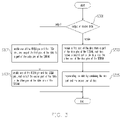
- FIG. 3 is a flowchart showing a data communication method of a SDRAM according to an embodiment of the present invention.
- step S 301 whether the data communication circuit 200 received the data from the SDRAM 220 or the data is output to the SDRAM 220 is determined.
- step S 303 wherein when the SDRAM 220 receives the data, the data input circuit 202 receives a first part of the data from a part of the data pins of the SDRAM, such as Q 0 –Qm, and then receives a second part of the data from the other part of the data pins of the SDRAM, such as Qm+1 ⁇ Qn.
- the data communication circuit 200 regenerates the data by combining the first part of the data and the second part of the data.
- the mask signal generating circuit 206 outputs a mask signal for enabling one of the UDQM pin and the LDQM pin, and the first part of the data is output to the part of the data pins, such as Q 0 –Qm.
- the mask signal generating circuit 206 outputs the mask signal for enabling the other one of the UDQM pin and the LDQM pin, and the second part of the data is output to the other part of the data pins, such as Qm+1 ⁇ Qn.
- the first part of the data comprises one of high address data and low address data
- the second part of the data comprises the remainder of the low address data or the high address data
- FIG. 4A is a schematic circuit block diagram of a data input circuit according to an embodiment of the present invention.
- the data input circuit 202 comprises a first D-type flip-flop circuit 401 and a second D-type flip-flop circuit 403 .
- the input of the first D-type flip-flop circuit 401 is coupled to the data bus DQ [7:0].
- the second D-type flip-flop circuit 403 receives an output DQ_DLY[7:0] of the first D-type flip-flop circuit 401 and the data bus DQ [7:0].
- FIG. 4B is a flowchart showing a data input method according to an embodiment of the present invention.
- FIG. 4C is a signal time sequence of the data input circuit of FIG. 4A .
- a period of a next preset clock signal T 1 is defined as a first period while the data input circuit 202 about to receive the data transmitted from the SDRAM at the period T 0 of the present clock signal CK.
- one of the UDQM pin and the LDQM pin is enabled during the first period T 1 .
- the first D-type flip-flop circuit 401 receives and locks the first part D 0 of the data from the data bus DQ[7:0].
- step S 405 another one of UDQM pin and the LDQM pin is enabled during the second period.
- the first D-type flip-flop circuit 401 outputs the first part D 0 of the data DQ_DLY[7:0] to the second D-type flip-flop circuit 403 .
- the second part D 1 of the data is transmitted from the data bus DQ[7:0] to the second D-type flip-flop circuit 403 through the output DQ_DLY[7:0] of the first D-type flip-flop circuit 401 .
- the second D-type flip-flop circuit 403 regenerates the data by combining the first part D 0 and the second part D 1 of the data and outputs the original data at the output terminal DIN[15:0].
- FIG. 5A is a schematic circuit block diagram of a data output circuit according to an embodiment of the present invention.
- the data communication circuit has a local bus DOUT[15:0] which has a width of 16 for transmitting data to the SDRAM.
- the input of the third D-type flip-flop circuit 501 is coupled to a part DOUT[15:8] of the local bus DOUT[15:0].
- the output DOUT_DLY[15:8] of the third D-type-flip-flop circuit 501 is coupled to the input terminal of the selector 503 .
- the other input terminal of the selector 503 is coupled to the other part DOUT[7:0] of the local bus DOUT[15:0].
- the output terminal DOUT_TMP[7:0] of the selector 503 is coupled to the fourth D-type flip-flop circuit 505 .
- the output terminal of the fourth D-type flip-flop circuit 505 is coupled to the data pins of the SDRAM through the data bus composed of the data lines. It is assumed that the number of the data lines, i.e. the width of the data bus, is 8.
- the selective terminal of the selector 503 receives the counting signal from the counter 507 for determining whether the output terminal DOUT_TMP[7:0] should be coupled to the input terminal DOUT[15:8] or DOUT[7:0].
- FIG. 5B is a flowchart showing a data output method according to an embodiment of the present invention.
- FIG. 5C is a signal time sequence of the data input circuit of FIG. 5A .
- a period of a next preset clock signal T 1 is defined as a first period while the data to be transmitted from the local bus DOUT[15:0] to the SDRAM at the period T 0 of the present clock signal CK.
- the first part D 0 of the data is transmitted from DOUT[7:0] of part of the local bus DOUT[15:0] to the selector 503 .
- the counter 507 outputs the counting signal so that the selector 503 transmits the first part D 0 of the data to the forth D-type-flip-flop directly and is locked during the period T 0 .
- the second part D 1 of the data is simultaneously transmitted from another part DOUT[15:8] of the local bus DOUT[15:0] to the third D-type flip-flop circuit 501 and is locked during the period T 0 .
- one of the UDQM pin and the LDQM pin of the SDRAM is enabled during the first period T 1 .
- the fourth D-type flip-flop circuit 505 outputs the first part D 0 of the data to the part of the data pins of the SDRAM through the data bus DQ[7:0].
- the third D-type flip-flop circuit 501 substantially simultaneously outputs the second part D 1 of the data to the selector 503 .
- the counter 507 outputs the counting signal so that the selector 503 outputs the second part D 1 of the data to the fourth D-type flip-flop circuit 505 and then the second part D 1 of the data is locked.
- another one of the UDQM pin and the LDQM is enabled during the second period T 2 .
- the fourth D-type flip-flop circuit 505 outputs the second part D 1 of the data to another part of the data pins of the SDRAM.
- FIG. 6 is a circuit block diagram showing a mask signal generating circuit according to an embodiment of the present invention.
- the mask signal generating circuit comprises a multiplexer 601 .
- the multiplexer 601 receives the mask signal DQM and then determines whether the mask signal DQM should be transmitted to the LDQM or the UDQM of the SDRAM according to the flag status stored, for example, in the flag register 603 .
- the present invention controls the UDQM pin and the LDQM pin of the SDRAM so as to divide the data into two parts for transmission.
- the data can be transmitted in two steps. Therefore, more data can be transmitted to the SDRAM using a data bus with a narrow width. Accordingly, the present invention can be adapted for low-capacity electronic devices.
Landscapes
- Dram (AREA)
- Semiconductor Integrated Circuits (AREA)
Abstract
Description
Claims (15)
Applications Claiming Priority (2)
| Application Number | Priority Date | Filing Date | Title |
|---|---|---|---|
| TW093121575A TWI242778B (en) | 2004-07-20 | 2004-07-20 | Circuitry and method of SDRAM for exchanging data |
| TW093121575 | 2004-07-20 |
Publications (2)
| Publication Number | Publication Date |
|---|---|
| US20060018178A1 US20060018178A1 (en) | 2006-01-26 |
| US7187618B2 true US7187618B2 (en) | 2007-03-06 |
Family
ID=35656962
Family Applications (1)
| Application Number | Title | Priority Date | Filing Date |
|---|---|---|---|
| US10/904,267 Expired - Fee Related US7187618B2 (en) | 2004-07-20 | 2004-11-02 | Circuit of SDRAM and method for data communication |
Country Status (2)
| Country | Link |
|---|---|
| US (1) | US7187618B2 (en) |
| TW (1) | TWI242778B (en) |
Families Citing this family (2)
| Publication number | Priority date | Publication date | Assignee | Title |
|---|---|---|---|---|
| US7546402B2 (en) * | 2005-03-24 | 2009-06-09 | Sunplus Technology Co., Ltd. | Optical storage system comprising interface for transferring data |
| EP2568390A1 (en) | 2011-09-08 | 2013-03-13 | ST-Ericsson SA | DRAM memory interface |
Citations (3)
| Publication number | Priority date | Publication date | Assignee | Title |
|---|---|---|---|---|
| US6496403B2 (en) * | 2000-07-31 | 2002-12-17 | Hitachi, Ltd. | Semiconductor memory device |
| US6867993B2 (en) * | 2000-07-21 | 2005-03-15 | Kabushiki Kaisha Toshiba | Semiconductor memory device |
| US6944092B2 (en) * | 2003-04-02 | 2005-09-13 | Hynix Semiconductor Inc. | Semiconductor memory device |
-
2004
- 2004-07-20 TW TW093121575A patent/TWI242778B/en not_active IP Right Cessation
- 2004-11-02 US US10/904,267 patent/US7187618B2/en not_active Expired - Fee Related
Patent Citations (3)
| Publication number | Priority date | Publication date | Assignee | Title |
|---|---|---|---|---|
| US6867993B2 (en) * | 2000-07-21 | 2005-03-15 | Kabushiki Kaisha Toshiba | Semiconductor memory device |
| US6496403B2 (en) * | 2000-07-31 | 2002-12-17 | Hitachi, Ltd. | Semiconductor memory device |
| US6944092B2 (en) * | 2003-04-02 | 2005-09-13 | Hynix Semiconductor Inc. | Semiconductor memory device |
Also Published As
| Publication number | Publication date |
|---|---|
| TWI242778B (en) | 2005-11-01 |
| US20060018178A1 (en) | 2006-01-26 |
| TW200605086A (en) | 2006-02-01 |
Similar Documents
| Publication | Publication Date | Title |
|---|---|---|
| US10762947B2 (en) | Memory devices | |
| US6459651B1 (en) | Semiconductor memory device having data masking pin and memory system including the same | |
| KR100499417B1 (en) | A method for masking the ringing in SDRAM and the device therefor | |
| US20100180143A1 (en) | Techniques for improved timing control of memory devices | |
| US6982924B2 (en) | Data output control circuit | |
| CN117193664A (en) | Apparatus and method including memory command for semiconductor memory | |
| US9218860B2 (en) | Multiple data rate memory with read timing information | |
| US7983095B2 (en) | Semiconductor memory apparatus | |
| US9324394B2 (en) | Strobe signal generation device and memory apparatus using the same | |
| US6920080B2 (en) | Methods for generating output control signals in synchronous semiconductor memory devices and related semiconductor memory devices | |
| US7546497B2 (en) | Semiconductor memory device and data write and read method thereof | |
| US6564287B1 (en) | Semiconductor memory device having a fixed CAS latency and/or burst length | |
| US6839291B2 (en) | Method for controlling column decoder enable timing in synchronous semiconductor device and apparatus thereof | |
| US8295100B2 (en) | Pipe latch circuit and method for operating the same | |
| US7295489B2 (en) | Method and circuit for writing double data rate (DDR) sampled data in a memory device | |
| US7706195B2 (en) | Strobe signal controlling circuit | |
| US9406357B2 (en) | Data capture system and method, and memory controllers and devices | |
| US7187618B2 (en) | Circuit of SDRAM and method for data communication | |
| US7995406B2 (en) | Data writing apparatus and method for semiconductor integrated circuit | |
| US7210017B2 (en) | Information processing apparatus, memory, information processing method, and program | |
| US20030188064A1 (en) | Register for the parallel-serial conversion of data | |
| US7898883B2 (en) | Method for controlling access of a memory | |
| KR100594294B1 (en) | Memory Device and Data Training Methods | |
| KR100615081B1 (en) | Dual data rate semiconductor memory device and data strobe signal output method | |
| US20050270853A1 (en) | Memory module and method for accessing the same |
Legal Events
| Date | Code | Title | Description |
|---|---|---|---|
| AS | Assignment |
Owner name: SUNPLUS TECHNOLOGY CO., LTD., TAIWAN Free format text: ASSIGNMENT OF ASSIGNORS INTEREST;ASSIGNORS:YANG, YING-CHIH;LIAO, JEN-YI;CHEN, YUAN-NING;AND OTHERS;REEL/FRAME:015318/0970 Effective date: 20041014 |
|
| STCF | Information on status: patent grant |
Free format text: PATENTED CASE |
|
| FPAY | Fee payment |
Year of fee payment: 4 |
|
| FPAY | Fee payment |
Year of fee payment: 8 |
|
| FEPP | Fee payment procedure |
Free format text: PAYOR NUMBER ASSIGNED (ORIGINAL EVENT CODE: ASPN); ENTITY STATUS OF PATENT OWNER: LARGE ENTITY |
|
| FEPP | Fee payment procedure |
Free format text: MAINTENANCE FEE REMINDER MAILED (ORIGINAL EVENT CODE: REM.); ENTITY STATUS OF PATENT OWNER: LARGE ENTITY |
|
| LAPS | Lapse for failure to pay maintenance fees |
Free format text: PATENT EXPIRED FOR FAILURE TO PAY MAINTENANCE FEES (ORIGINAL EVENT CODE: EXP.); ENTITY STATUS OF PATENT OWNER: LARGE ENTITY |
|
| STCH | Information on status: patent discontinuation |
Free format text: PATENT EXPIRED DUE TO NONPAYMENT OF MAINTENANCE FEES UNDER 37 CFR 1.362 |
|
| FP | Lapsed due to failure to pay maintenance fee |
Effective date: 20190306 |