US7158455B2 - Servo error detecting device for optical disk - Google Patents
Servo error detecting device for optical disk Download PDFInfo
- Publication number
- US7158455B2 US7158455B2 US10/339,376 US33937603A US7158455B2 US 7158455 B2 US7158455 B2 US 7158455B2 US 33937603 A US33937603 A US 33937603A US 7158455 B2 US7158455 B2 US 7158455B2
- Authority
- US
- United States
- Prior art keywords
- signal
- envelope
- signals
- light receiving
- difference
- Prior art date
- Legal status (The legal status is an assumption and is not a legal conclusion. Google has not performed a legal analysis and makes no representation as to the accuracy of the status listed.)
- Expired - Lifetime
Links
Images


Classifications
-
- G—PHYSICS
- G11—INFORMATION STORAGE
- G11B—INFORMATION STORAGE BASED ON RELATIVE MOVEMENT BETWEEN RECORD CARRIER AND TRANSDUCER
- G11B7/00—Recording or reproducing by optical means, e.g. recording using a thermal beam of optical radiation by modifying optical properties or the physical structure, reproducing using an optical beam at lower power by sensing optical properties; Record carriers therefor
- G11B7/08—Disposition or mounting of heads or light sources relatively to record carriers
- G11B7/09—Disposition or mounting of heads or light sources relatively to record carriers with provision for moving the light beam or focus plane for the purpose of maintaining alignment of the light beam relative to the record carrier during transducing operation, e.g. to compensate for surface irregularities of the latter or for track following
- G11B7/094—Methods and circuits for servo offset compensation
-
- G—PHYSICS
- G11—INFORMATION STORAGE
- G11B—INFORMATION STORAGE BASED ON RELATIVE MOVEMENT BETWEEN RECORD CARRIER AND TRANSDUCER
- G11B7/00—Recording or reproducing by optical means, e.g. recording using a thermal beam of optical radiation by modifying optical properties or the physical structure, reproducing using an optical beam at lower power by sensing optical properties; Record carriers therefor
- G11B7/08—Disposition or mounting of heads or light sources relatively to record carriers
- G11B7/085—Disposition or mounting of heads or light sources relatively to record carriers with provision for moving the light beam into, or out of, its operative position or across tracks, otherwise than during the transducing operation, e.g. for adjustment or preliminary positioning or track change or selection
- G11B7/08505—Methods for track change, selection or preliminary positioning by moving the head
- G11B7/08511—Methods for track change, selection or preliminary positioning by moving the head with focus pull-in only
Abstract
Servo error signal circuitry apparatus and methods are described. The difference between two bottom envelope signals SEbtm and SFbtm is calculated by a subtracter (40) to generate a difference signal (SEbtm−SFbtm). The difference signal (SEbtm−SFbtm) is input as an alignment signal (AL) to an equalizer (42) and as a basic tracking error signal to the positive input terminal of a second subtracter (52). On the other hand, the difference between two top envelope signals SEtop and SFtop is calculated by a third subtracter (48) to generate a difference signal (SEtop−SFtop). The signal K(SEtop−SFtop) obtained by multiplying a coefficient K with the difference signal using a coefficient multiplier (50) is input to the negative input terminal of the second subtracter (52). The difference signal {(SEbtm−SFbtm)−K(SEtop−SFtop)} output from the second subtracter (52) is used as an offset corrected tracking error signal.
Description
The present invention relates generally to a servo mechanism in an optical disk device; and, in particular, a servo error detecting device and method used for detecting positional or optical errors of the positioning of a light beam used for reading an optical disk.
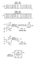
A light pick-up 14 that can move in the radial direction of the disk is set opposite the signal recording side 10 a of optical disk 10. Light pick-up 14 focuses and radiates a laser beam LB onto the signal recording side 10 a of optical disk 10, detects the light beam reflected from signal recording side 10 a, performs photoelectric transformation, and generates an electric signal having a waveform corresponding to the embossment pattern of the pit arrays. The electric signal output from light pick-up 14 is sent to an RF amplifier 16. RF amplifier 16 generates a reproduced data signal SM, as well as a tracking error signal TE and a focus error signal FE. The reproduced data signal SM output from RF amplifier 16 is input to a data signal processing unit (not shown in the figure), where decoding, error correction, or other signal processing is performed. A servo error signal, such as the tracking error signal TE or focus error signal FE, output from RF amplifier 16 is sent to a pick-up servo 18. Pick-up servo 18 performs tracking control for positioning or tracking the beam spot SP of laser beam LB on the track (pit array) and also performs focusing control for focusing beam spot SP to the size of the pit.
The RF signals SA and SD obtained from light receiving regions A and D on the left side of the boundary that is the central line in parallel with the track direction have the same phase. The RF signals SB and SC obtained from the light receiving regions B and C on the right side of the same boundary also have the same phase. The RF signals SA, SD have opposite phases from RF signals SB, SC.
When the beam spot SP of laser beam LB on signal recording side 10 a of optical disk 10 is positioned on the track center, that is, when it is on track, the light beam LB′ reflected from signal recording side 10 a is incident onto the central part of the light receiving regions A, B, C, D of the light detector. The level of the RF signals SA and SD obtained from the light receiving regions A and D on the left side is almost the same as that of the RF signals SB and SC obtained from the light receiving regions B and C on the right side.
However, when beam spot SP shifts from the center of the track in the radial direction, the reflected light beam LB′ is incident onto a position that deviates to the left or right from the central part of the light receiving regions A, B, C, D of the light detector. The level of the RF signals SA and SD obtained from the light receiving regions A and D on the left side becomes different from that of the RF signals SB and SC obtained from the light receiving regions B and C on the right side. For example, if beam spot SP shifts inward in the radial direction, the focusing position of the reflected light beam LB′ is offset to the left side of light receiving regions A, B, C, D. The level of the RF signals SA and SD obtained from the light receiving regions A and D on the left side becomes higher than that when the beam spot is on track. On the other hand, the level of the RF signals SB and SC on the side of right-side light receiving regions B and C becomes lower than that when the beam spot is on track. If beam spot SP shifts outward in the radial direction, the focusing position of reflected light beam LB′ is offset to the right side of the light receiving regions A, B, C, D. The level of the RF signals SB and SC obtained from the right-side light receiving regions B and C becomes higher than that when the beam spot is on track, while the level of the RF signals SA and SD obtained from the left-side light receiving regions A and D becomes lower than that when the beam spot is on track.
According to the astigmatism method, when the objective lens in light pick-up 14 is too close to optical disk 10, the spot of the reflected light beam focused onto the light receiving region A, B, C, D of the light detector becomes an elliptic shape that is stretched on the side of light receiving regions A and C and is compressed on the side of light receiving regions B and D, as shown by broken line LBa in FIG. 6 . On the other hand, when the objective lens is too far away from optical disk 10, the spot of the reflected light beam focused in the light receiving region A, B, C, D of the light detector becomes an elliptic shape that is stretched on the side of light receiving regions B and D and is compressed on the side of light receiving regions A and C, as shown by dot-dashed line LBb in FIG. 6 .
In an optical disk device, the accuracy of a servo error signal, such as the tracking error signal TE or the focus error signal FE, controls the accuracy of the servo. For example, for a tracking servo, when the light pick-up is jump-shifted from the track during the current tracking to another track, if the accuracy of the tracking error signal is low, a long time will be required from applying the tracking servo near the targeted track until reaching the state of on-track, or it is difficult to correctly perform an on-track operation.
In a conventional tracking error detecting circuit (FIG. 4 ), operation circuits 200, 202, 204 perform the required operation (push-pull operation) for the RF signals SA, SB, SC, SD obtained from the light receiving regions A, B, C, D of the light detector, respectively. In this way, tracking error signal TE that indicates the positional error of beam spot SP in the radial direction can be obtained. However, whether in low-speed or high-speed playback, as a result of passing through the low-pass filter, the tracking signal TE is attenuated significantly (by about one-half), leading to deterioration in the SN (signal-to-noise) characteristic (see FIGS. 8 and 9 ). The reason for this is that the top envelope component of the RF signal is almost flat. Also, in the case of low-speed playback, the frequency of the RF signal is relatively close to that of the tracking error signal. It is difficult to separate the two signals using a low-pass filter. The RF signal component tends to be left over in the tracking error signal TE as shown in FIG. 8 .
In general optical disks, such as a CD (Compact Disc) and a DVD (Digital Versatile Disk), EFM (eight to fourteen modulation) or EFM Plus is usually used as the modulation method for the data recorded on the tracks. The length of the pits is limited to the range of 3T–11T (T is the length of one bit) in order to satisfy the [2, 10] RLL (Run-Length Limited) code condition, that is, the length of “0” is in the range of 2–11. Therefore, for example, in a CD, the frequency of the channel clock is 4.32 MHz at double speed. However, the frequency of the RF signal reaches the highest level of 720 kHz in the case of 3T/3T. It is as low as 196 kHz in the case of 11T/11T. In order to perform tracking servo correctly, such an RF signal component in the tracking error signal is desired to be so small that it can be ignored.
In the conventional tracking error detecting circuit, however, it is difficult to separate or cut the RF signal component with a frequency of about 196 kHz from the tracking error signal TE obtained from the tracking modulation component Ste that usually has a frequency of tens of kHz by passing the signal through low-pass filter 106.
Also, in order to match the input range of the AD converter (not shown in the figure) in a later stage during conversion to digital signals, the amplitude of the tracking error signal TE is increased by using operation circuits 200, 202, 204 or a special gain control amplifier (not shown in the figure). However, since the RF signal component is also amplified, the gain cannot be increased sufficiently. In addition, the accuracy of the digital signal becomes low due to mixing of the RF signal component.
On the other hand, during high-speed playback performed at 30-fold speed for a CD or 6-fold speed for a DVD, the band of the RF signal becomes 10 MHz or higher. When the band of operation circuits 200, 202, 204 is only several MHz, these operation circuits act as low-pass filters. They not only attenuate the RF signal component but also reduce the tracking error signal TE by half to its original form, that is, to the tracking modulation component Ste. As a result, SN becomes as low as 6 dB.
In a conventional focus error detecting circuit (FIG. 5 ), the accuracy of the focus error signal and SN are also low. Other servo error detecting systems using light detectors other than the four-division type also have the same problem.
There is a need to solve the problem of the conventional technology by providing a servo error detecting device for an optical disk that can generate error signals for servo, from which the high-frequency component can be effectively cut off.
There is also a need to provide a servo error detecting device for an optical disk that can generate error signals for a servo with a high SN ratio.
In accordance with one aspect of the invention, a first implementation of servo error detecting device for an optical disk is used to detect errors on the positional or optical servo of a light beam on the signal recording side of an optical disk. The servo error detecting device has an optical detector that receives a light beam reflected from the signal recording side of the optical disk in one or multiple light receiving regions and outputs an electric signal corresponding to the light intensity of the reflected light beam, an envelope detector that detects the top envelope and/or bottom envelope of each of the electric signals and generates a top envelope signal and/or bottom envelope signal representative of the waveform of the top envelope and/or bottom envelope, and a servo error signal generator that processes the top envelope signal and/or bottom envelope signal to generate a servo error signal.
In the described first servo error detecting device, appropriate processing is performed to convert the high-frequency electric signal output from each light receiving region of the light detector to a low-frequency top envelope signal and/or bottom envelope signal, effectively removing or rendering negligible the high-frequency component, and enabling a servo error signal with an excellent SN characteristic to be obtained.
In one embodiment, a servo error signal generator calculates the difference between the bottom envelope signal obtained from a first light receiving region and the bottom envelope signal obtained from a second light receiving region to generate a tracking error signal that indicates the tracking error. In order to compensate the offset caused by displacement of the optical disk or dislocation of the optical system, a bottom envelope signal correcting circuit is used that corrects each of the bottom envelope signals obtained from the first and second light receiving regions by subtracting the corresponding top envelope signal from it. The bottom envelope signal correction may be done by a first coefficient multiplier that multiples a desired coefficient with the top envelope signal before the subtraction.
The servo error detecting device may also have a top envelope differential signal generator, which calculates the difference between the top envelope signals obtained from the first and second light receiving regions to generate a top envelope differential signal, and have offset correction to correct the offset of the tracking error signal depending on the top envelope differential signal. In this case, the servo error detecting device may have a second coefficient multiplier that multiplies a desired coefficient with each of the top envelope signals or a third coefficient multiplier that multiplies a desired coefficient with the top envelope differential signal.
In another embodiment, the servo error signal generator may have an equalizer circuit, which selectively amplifies or attenuates a desired frequency band component for the difference signal obtained by calculating the difference between the bottom envelope signal obtained from the first light receiving region and the bottom envelope signal obtained from the second light receiving region, and utilize frequency characteristic adjustment to adjust the frequency characteristic of the tracking error signal based on the output signal of the equalizer circuit.
In accordance with another aspect of the invention, a second implementation of servo error detecting device for an optical disk provided is used to detect errors on the positional or optical servo of a light beam on the signal recording side of an optical disk. The servo error detecting device has an optical detecting means that receives a light beam reflected from the signal recording side of the optical disk in a first group and a second group of light receiving regions and outputs multiple electric signals corresponding to the light intensity of the reflected light beam in each of the light receiving regions of each group, an envelope detector that detects the top envelopes and/or bottom envelopes of the multiple electric signals and generates multiple top envelope signals and/or bottom envelope signals representative of the waveform of each of the top envelopes and/or bottom envelopes, and a servo error signal generator that processes the multiple top envelope signals and/or bottom envelope signals to generate servo error signals.
In the described second servo error detecting device, appropriate processing is performed to convert the multiple high-frequency electric signals output from each of the first and second groups of light receiving regions of the light detector to a low-frequency top envelope signal and/or bottom envelope signal, effectively removing or rendering negligible the high-frequency component, and enabling a servo error signal with an excellent SN characteristic to be obtained.
In a described embodiment, the first and second groups of light receiving regions are arranged in an opposite phase mode using a push-pull method. The servo error signal generator has a first adder that calculates the sum of the multiple bottom envelope signals obtained from the first group of light receiving regions to generate a first sum signal, a second adder that calculates the sum of the multiple bottom envelope signals obtained from the second group of light receiving regions to generate a second sum signal, and a tracking error signal generator that calculates the difference between the first and second signals to generate a tracking error signal that indicates the tracking error.
In another embodiment, the first and second groups of light receiving regions are arranged in an opposite phase mode using an astigmatism method. The servo error signal generator has a first adder that calculates the sum of the multiple bottom envelope signals obtained from the first group of light receiving regions to generate a first sum signal, a second adder that calculates the sum of the multiple bottom envelope signals obtained from the second group of light receiving regions to generate a second sum signal, and a focus error signal generator that calculates the difference between the first and second sum signals to generate a focus error signal that indicates the focusing error.
In another aspect of the invention, a third implementation of servo error detecting device is used to detect errors on the positional or optical servo of a light beam on the signal recording side of an optical disk. The servo error detecting device has an optical detector that receives a light beam reflected from the signal recording side of the optical disk in a first group and a second group of light receiving regions and outputs multiple electric signals corresponding to the light intensity of the reflected light beam in each of the light receiving regions of each group, a first electric signal combiner combines the multiple electric signals obtained from the first group of light receiving regions to generate a first combined electric signal, a second electric signal combiner combines the multiple electric signals obtained from the second group of light receiving regions to generate a second combined electric signal, an envelope detector detects the top envelopes and/or bottom envelopes of the first and second combined electric signals and generates multiple top envelope signals and/or button signals representative of the waveform of each of the top envelopes and/or bottom envelopes, and a servo error signal generator processes the multiple top envelope signals and/or bottom envelope signals to generate desired servo error signals.
In the described third servo error detecting device, the multiple high-frequency electric signals output from each of the first and second groups of light receiving regions of the light detector are combined for each group, and a required processing is carried out to convert each of the combined signals to a low-frequency top envelope signal and/or bottom envelope signal. High-frequency components are minimized, and a servo error signal with an excellent SN characteristic can be obtained.
Implementations of the invention are described with reference to the accompanying figures and in the context of an optical disk apparatus having the basic configuration previously described and shown in FIG. 1 .
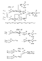
A first implementation utilizes an arrangement of light receiving regions of a light detector shown in FIG. 10 . Such light detector is typical of a so-called three-beam system. A pair of light receiving regions E and F are arranged at a prescribed distance on the left and right sides of the four-division light receiving regions A, B, C, D. In the three-beam system, a pair of secondary beams LBE and LBF are focused and radiated in the radial direction from light pick-up 14 (see FIG. 1 ) to the signal recording side 10 a of optical disk 10 at a prescribed interval. The main beam LB is sandwiched between them. The beam LB′ of the light reflected from signal recording side 10 a corresponding to the main beam LB is focused and incident onto the central light receiving regions A, B, C, D. The beams LBE′ and LBF′ of the returning or reflected light corresponding to secondary beams LBE′ and LBF′ are focused and incident onto the light receiving regions E and F on the left and right sides, respectively. Light receiving regions A, B, C, D, E, F generate electric signals or RF signals SA, SB, SC, SD, SE, SF, respectively, corresponding to the quantity or intensity of the received light. These RF signals may be voltage signals obtained as a result of I–V conversion performed in pick-up 14. The level of a reference voltage Vc applied as a bias voltage from outside to the pickup is used as the reference.
With the same reference voltage Vc applied to light pick-up 14 used as a reference level, gain control amplifiers 20A–20F amplify the RF signals SA−SF at desired gains, respectively. As a result of this gain amplification, amplitude error depending on the type of optical disk can also be absorbed, and the reference level of the RF signals can be aligned with a prescribed value.
Basically, the difference signal (SEbtm−SFbtm) output from subtracter 26 can be used as the tracking error signal for a three-beam system. In this embodiment, the difference signal passes through gain control amplifier 28 and offset circuit 30 sequentially, where the signal is subjected to gain adjustment and offset adjustment for the tracking error. Then, the signal is output as tracking error signal TE and is supplied to an A/D converter (not shown in the figure) in a later stage. For example, if the input range of the A/D converter is 2 V, the amplitude of the tracking error signal TE is amplified to about 1.5 V by gain control amplifier 28. Since the tracking error signal TE essentially contains no RF signal component and the SN ratio is high, a good waveform can be maintained even after amplification. In this way, a highly accurate tracking error signal can be obtained. It is also possible to pass the tracking error signal TE through a low-pass filter or anti-aliasing circuitry (not shown in the figure) before inputting it into the A/D converter.
During track jump, as shown in FIG. 14 , tracking servo is performed with the tracking error signal TE used as a feedback signal after entering an interval of 180° before and after the desired on-track position TRon, i. According to this embodiment, since the accuracy of the tracking error signal TE is high, the beam spot can be shifted to the targeted track quickly and correctly.
The tracking error detecting circuit has a circuit used for compensating the offset corresponding to the change in the top level of each RF signal SE and SF. The offset compensating circuit is comprised of coefficient multipliers 32, 34 and subtracters 36, 38.
More specifically, the bottom envelope signal SEbtm output from bottom envelope circuit 24E is input to the positive input terminal of subtracter 36, while the top envelope signal SEtop output from top envelope circuit 22E is input to coefficient multiplier 32. The output signal K•SEtop of coefficient multiplier 32 is supplied to the negative input terminal of subtracter 36. In this case, K is a multiplication coefficient set in coefficient multiplier 32. Subtracter 36 calculates the difference between the two input signals and outputs the different signal (SEbtm−K•SEtop) as compensated bottom envelope signal SEbtm′.
Also, the bottom envelope signal SFbtm output from bottom envelope circuit 24F is input to the positive input terminal of subtracter 38, while the top envelope signal SFtop output from top circuit 22F is input to coefficient multiplier 34. The output signal K•SFtop of coefficient multiplier 34 is supplied to the negative input terminal of subtracter 38. The same multiplication coefficient K as that of coefficient multiplier 32 is set in coefficient multiplier 34. Subtracter 38 calculates the difference between the two input signals and outputs the difference signal (SFbtm−K•SFtop) as corrected bottom envelope signal SFbtm′.
For the RF signal, when the top level oscillates, as shown in FIGS. 16A–16C , the oscillation component also affects the bottom level. As a result, an offset corresponding to the oscillation of the top level appears in the tracking modulation component Ste on the bottom side. In this embodiment, the top level change Stw in the RF signal is separated in the state of top envelope signal Stop. The signal K•SFtop obtained by multiplying an appropriate coefficient K with top envelope signal Stop is used as the offset component, which is subtracted from bottom envelope signal Sbtm. In this way, offset of the tracking modulation component Ste corresponding to the top level change Stw is cancelled out.
In this way, in FIG. 15 , both the corrected bottom envelope signals SEbtm′ and SFbtm′ output from subtracters 36 and 38 almost contain no RF signal component, and influence (offset) of the top level can be eliminated. Consequently, there is almost no RF signal component in the finally obtained tracking error signal TE, and the influence of the top level can be eliminated.
In this embodiment, there is also a circuit used for adjusting the frequency characteristic of the tracking error signal TE. The frequency characteristic adjusting circuit is comprised of subtracter 40, equalizer 42, and gain control amplifier 44. Subtracter 40 calculates the difference between the two bottom envelope signals SEbtm and SFbtm and outputs the difference signal (SEbtm−SFbtm) as alignment signal AL. Equalizer 42 emphasizes (amplifies) or attenuates the desired frequency band component to change the frequency characteristic of the alignment signal AL. After the gain of the alignment signal AL with the desired frequency characteristic is adjusted by gain control amplifier 44, the signal is added by adder 46 to basic tracking error signal (SEbtm′−SFbtm′) output from subtracter 26. Since the alignment signal AL essentially contains no RF signal component, the frequency characteristic of the tracking error signal TE can be adjusted without lowering SN.
(SEbtm−SFbtm)−K(SEtop−SFtop)=(SEbtm−K•SEtop)−(SFbtm−K•SFtop) (1)
In the embodiment shown in FIG. 17 , a center error detecting circuit is comprised of subtracter 48, gain control amplifier 54, and offset circuit 56. Subtracter 48 is shared with the tracking error detecting circuit. It calculates the difference between two top envelope signals SEtop and SFtop and outputs the difference signal (SEtop−SFtop). The difference signal (SEtop−SFtop) passes through gain control amplifier 54 and offset circuit 56, where gain adjustment and offset adjustment used for the center error are performed for the signal. The obtained signal is then supplied as a center error signal CE to an A/D converter (not shown in the figure) in a later stage. The center error signal CE essentially contains no RF signal component. It can be used as a servo error signal that indicates the positional error of light pick-up 14 in the radial direction.
The focus error detecting circuit is comprised of adders 60, 62, coefficient multiplier 64, subtracter 66, gain control amplifier 68, and offset circuit 70. Adder 60 receives the inputs of top envelope signals SAtop and SCtop output from top envelope circuits 22A and 22C corresponding to light receiving regions A and C, calculates the sum of the two input signals, and outputs the sum signal (SAtop+SCtop). The sum signal (SAtop+SCtop) is multiplied with a desired coefficient K in coefficient multiplier 64 and is then input to the positive input terminal of subtracter 66. The other adder 62 receives the inputs of top envelope signals SBtop and SDtop output from top envelope circuits 22B and 22D corresponding to light receiving regions B and D, calculates the sum of the two input signals, and outputs the sum signal (SBtop+SDtop). The sum signal (SBtop+SDtop) is input to the negative input terminal of subtracter 66. Subtracter 66 calculates the difference between the two input signals and outputs difference signal {K(SAtop+SCtop)−(SBtop+SDtop)}. Basically, the difference signal output from subtracter 66 can be used as the focus error signal. In this embodiment, the difference signal passes through amplifier 68 and offset circuit 70, where the gain adjustment and offset adjustment used for the focus error FE are performed for the signal. The obtained signal is supplied to an A/D converter (not shown in the figure) in a later stage. It is also possible to omit coefficient multiplier 64 and input the output of adder 60 directly to subtracter 66.
In the astigmatism method, if the objective lens in pick-up 14 is too close to disk 10 (see FIG. 1 ), the levels of the RF signals SA and SC generated from light receiving regions A and C in the light detector are higher than those of the RF signals SB and SD generated from light receiving regions B and D. The focus error signal FE is offset to the positive side. On the other hand, if the objective lens in pick-up 14 is too far away from disk 10, the levels of RF signals SB and SD are higher than those of RF signals SA and SC, and the focus error signal FE is offset to the negative side. In this way, focusing servo is performed appropriately so that the level of focus error signal FE approaches zero. In this embodiment, since the focus error signal FE essentially contains no RF signal component and the SN ratio is high, highly-accurate focusing servo can be performed.
In FIG. 18 , the pull-in circuit is comprised of adders 60, 62, adder 72, gain control amplifier 74, and offset circuit 76. Adders 60 and 62 are shared with the focus error detecting circuit. Adder 72 adds the signal (SAtop+SCtop) output from adder 60 to the signal (SBtop+SDtop) output from adder 62 and outputs the total sum signal (SAtop+SCtop+SBtop+SDtop). Basically, the total sum signal can be used as a pull-in signal. In this embodiment, the pull-in signal passes through gain control amplifier 74 and offset circuit 76, where the gain adjustment and offset adjustment used for pull-in are performed for the circuit. The obtained signal is output as a pull-in signal PI to an A/D converter (not shown in the figure) in a later stage.
The level of the pull-in signal PI changes corresponding to the distance between pick-up 14 and optical disk 10. In other words, as pick-up 14 is moved closer to optical disk 10, the levels of the RF signals SA, SB, SC, SD become higher. Therefore, the level of pull-in signal PI becomes higher. For example, during initialization immediately after the power is turned on, pick-up 14 can be moved closer to optical disk 10 with pull-in signal PI used as a monitor signal. Since the pull-in PI signal essentially contains no RF signal and the SN ratio is high, a stable and reliable pick-up starting operation can be performed.
The bottom envelope signals SAbtm and SDbtm obtained from bottom envelope circuits 24A and 24D (see FIG. 11 ) corresponding to the light receiving regions A and D of the light detector are input to adder 80, which outputs the sum signal (SAbtm+SDbtm) that indicates the sum of the two input signals. The sum signal (SAbtm+SDbtm) essentially contains no RF signal component. Also, since the two bottom envelope signals SAbtm and SDbtm are in phase, the peak-to-peak value of the sum signal (SAbtm+SDbtm) is doubled.
The bottom envelope signals SBbtm and SCbtm obtained from bottom envelope circuits 24B and 24C (FIG. 11 ) corresponding to the light receiving regions B and C of the light detector are input to another adder 82, which outputs the sum signal (SBbtm+SCbtm) that indicates the sum of the two input signals. The sum signal (SBbtm+SCbtm) essentially contains no RF signal component. Also, since the two bottom envelope signals SBbtm and SCbtm are in phase, the peak-to-peak value of the sum signal (SBbtm+SCbtm) is doubled.
The sum signal (SAbtm+SDbtm) output from adder 80 and the sum signal (SBbtm+SCbtm) output from adder 82 are input to the positive and negative terminals of subtracter 84, respectively. The subtracter outputs the difference signal {(SAbtm+SDbtm)−(SBbtm+SCbtm)} that indicates the difference between the two input signals. The difference signal essentially contains no RF signal component. Since the two sum signals (SAbtm+SDbtm) and (SBbtm+SCbtm) are out of phase, the peak-to-peak value of the difference signal is doubled.
Basically, the difference signal {(SAbtm+SDbtm)-(SBbtm+SCbtm)} output from subtracter 84 can be used as the tracking error signal of the push-pull system. However, it is also possible to supply the signal to an A/D converter (not shown in the figure) after passing it through a gain control amplifier, offset circuit, or low-pass filter (not shown in the figure).
The light receiving regions A1, A3, A4, A2 in the first stage generate electric signals or RF signals SA1, SA3, SA4, SA2 corresponding to the quantity or intensity of the received light. These RF signals may be voltage signals obtained as a result of I–V conversion performed in pick-up 14. The level of a reference voltage Vc applied as a bias voltage from outside to the pick-up is used as the reference.
More specifically, the RF signals SA1, SA2, SA3, SA4 obtained from the light receiving regions A1, A2, A3, A4 in the first stage are input to top envelope circuits 92A1, 92A2, 92A3, 92A4 and bottom envelope circuits 94A1, 94A2, 94A3, 94A4 via gain control amplifiers 90A1, 90A2, 90A3, 90A4, respectively. The RF signals SB1, SB2, SB3, SB4 obtained from the light receiving regions B1, B2, B3, B4 in the second stage are input to top envelope circuits 92B1, 92B2 92B3, 92B4 and bottom envelope circuits 94B1, 94B2, 94B3, 94B4 via gain control amplifiers 90B1, 90B2, 90B3, 90B4, respectively.
Top envelope circuits 92A1–92A4, 92B1–92B4, for example, are comprised of capacitor-type peak hold circuits. They can detect the top envelopes of RF signals SA1–SA4, SB1–SB4 and output signals SA1top–SA4top, SB1top–SB4top that express the respective top envelope waveforms. The droop rate of the peak hold circuit in each top envelope circuit is set at an appropriate value so that it can follow the top envelope waveform of the RF signal.
Bottom envelope circuits 94A1–94A4, 94B1–94B4, for example, are comprised of capacitor-type peak hold circuits. They can detect the bottom envelopes of RF signals SA1–SA4, SB1–SB4 and output signals SA1btm–SA4btm, SB1btm–SB4btm that express the respective bottom envelope waveforms. The droop rate of the peak hold circuit in each bottom envelope circuit is set at an appropriate value so that it can follow the bottom envelope waveform of the RF signal.
Both of the first and second bottom envelope signals SEbtm and SFbtm almost contain no RF signal component, and the tracking modulation components included in the RF signals are expressed at a high SN ratio. Consequently, when the two bottom envelope signals SEbtm and SFbtm are supplied, for example, to the tracking error detecting circuit shown in FIG. 12 , a tracking error signal TE of the TPP method with a high SN ratio can be obtained according to the present invention.
On the other hand, a first top envelope sum signal SEtop (SA2top+SA4top+SB1top+SB3top) and a second top envelope sum signal SFtop (SA1top+SA3top+SB2top+SB4top) can also be obtained using the same sum signal generating circuit as that shown in FIG. 23 . Consequently, it is also possible to use the tracking error detecting circuit shown in FIG. 15 or 17 with the first and second bottom sum signals SEbtm, SFbtm and the first and second top envelope sum signals SEtop, SFtop used as the input signals.
The second sum signal generating part has the same circuit configuration as the first sum signal generating part. The RF signals SA1, SA3, SB2, SB4 obtained from light receiving regions A1, A3, B2, B4 that are in phase are input to the sum signal generating part, which outputs the second RF sum signal SF (SA1+SA3+SB2+SB4) from combining circuit 126. The second bottom envelope signal SFbtm that expresses the bottom envelope waveform of the second RF sum signal SF is output from bottom envelope circuit 128.
Both of the first and second bottom envelope sum signals SEbtm and SFbtm almost contain no RF signal component and are essentially equivalent to the sum signals shown in FIG. 14 . Consequently, they can be used as the input signals of the tracking error detecting circuit shown in FIG. 12 , 15, or 17.
For top envelope signals, by connecting a first and a second top envelope circuit (not shown in the figure) to the outputs of combining circuits 116 and 126, the first top envelope sum signal SEtop that expresses the top envelope waveform of the first sum signal SE is output from the first envelope circuit, and the second top envelope sum signal SFtop that expresses the top envelope waveform of the second sum signal SF is output from the second envelope circuit. The first and second top envelope sum signals SEtop and SFtop can be used as the input signals of the tracking error detecting circuit shown in FIG. 15 or 17.
As described above, in the present invention, a top envelope and/or bottom envelope are/is extracted from the electric signals or RF signals obtained from the light pick-up or light detector. The RF signal components can be effectively cut off to obtain highly-accurate servo error signals with excellent SN characteristics by performing a required processing for the extracted top envelope and/or bottom envelope. Also, since the required signal components contained in the RF signals required for various types of servo can be converted to low-frequency signals without lowering their levels, there is no need to use a high frequency band circuit.
In the following, real waveform models are used to explain the difference between the system of the present invention that extracts a bottom envelope from an RF signal and a conventional system that simply passes an RF signal through a low-pass filter from the aspect of the frequency spectrum obtained by means of Fourier transformation.
First, as shown in FIG. 25A , a model obtained by simply overlapping a low-frequency modulation component MOD(t) (envelope component) with an RF signal RF(t) with a constant amplitude is taken into consideration. Signal f(t) of this model is defined by equation (2).
In this case, ARF and ωRF represent the amplitude and frequency of RF signal RF(t), respectively. AMOD and ωMOD represent the amplitude and frequency of the low-frequency modulation component MOD(t), respectively. When Fourier transformation is performed, said equation (2) becomes the following equation (3). The integration interval of each integration symbol ∫ is −∞−+∞.
Then, as shown in FIG. 26A , a model of bottom modulation obtained by overlapping a low-frequency modulation component MOD(t) with only the bottom side of an RF signal RF(t) with a constant amplitude is taken into consideration. Signal f(t) of this model is defined by the following equation (4).
In equation (4), ARF and ωRF represent the amplitude and frequency of RF signal RF(t), respectively, AMOD and ωMOD represent the amplitude and frequency of the low-frequency modulation component MOD(t), respectively. When Fourier transformation is performed, said equation (4) becomes the following equation (5). The integration interval of each integration symbol ∫ is −∞−+∞.
When specific values (ARF=1/2, AMOD=0.4/2) are substituted into the equation to compare each coefficient, the following is obtained.
On the other hand, when Fourier transformation is performed directly for 0.4/2 cos ωt (bottom envelope component in FIG. 26A ), the following is obtained.
H(jω)=0.2πδ(ω−ωMOD)+0.2πδ(ω+ωMOD) (7)
H(jω)=0.2πδ(ω−ωMOD)+0.2πδ(ω+ωMOD) (7)
As can be seen from equations (6) and (7), in a conventional system and the system of the present invention, the amplitude of ωMOD spectrum has a relationship of 0.1 and 0.2, that is, a ratio of 1:2.
The embodiments described above pertain to a servo error signal generating circuit for generating tracking error signal, focus error signal, center error signal, and pull-in signal. The present invention, however, is not limited to the servo error signal generating circuits described in these embodiments. It is applicable to circuits and servo error detecting systems for generating various types of servo error signals. Also, the technologies used in the present invention may have various modifications. In particular, the light detecting means, envelope detecting means, and operation means are not limited to those described above. Other systems or configurations can also be adopted.
In the present invention, the envelope component is extracted from an RF signal without passing the RF signal through a low-pass filter, and a tracking error signal is obtained from the extracted envelope component. Therefore, the signal component is not attenuated. As a result, the SN ratio can be increased compared with that in a conventional method.
As explained above, by using the servo error detecting device for an optical disk disclosed in the present invention, the high-frequency component can be effectively cut off to obtain a highly-accurate servo error signal with an excellent SN characteristic.
Those skilled in the art to which the invention relates will appreciate that yet other substitutions and modifications may be made to the described embodiments, without departing from the spirit and scope of the invention and set forth in the description and the claims.
Claims (2)
1. A servo error detector for an optical disk having a signal recording side, comprising:
an optical detector for receiving light reflected from the signal recording side of the optical disk in multiple light receiving regions and generating electric signals corresponding to the light intensity of the reflected light in each of the light receiving regions,
an envelope detector for detecting the top envelope and bottom envelope of each of the electric signals and generating a top envelope signal and a bottom envelope signal for each of the electric signals, and
a servo error signal generator circuit for processing the top envelope signals and bottom envelope signals to generate a servo error signal,
wherein the servo error signal generating circuit calculates the difference between the bottom envelope signal obtained from a first light receiving region and the bottom envelope signal obtained from a second light receiving region to generate an alignment signal, calculates the difference between the top envelope signal obtained from the first light receiving region and the top envelope signal obtained from the second light receiving region to generate a top envelope difference signal, calculates the difference between the alignment signal and the top envelope difference signal to generate a first difference signal, equalizes the alignment signal, and combines the first difference signal and the equalized alignment signal to generate the servo error signal.
2. The servo error detector of claim 1 , wherein the servo error signal generating circuit processes the top envelope difference signal to generate a center error signal.
Applications Claiming Priority (2)
| Application Number | Priority Date | Filing Date | Title |
|---|---|---|---|
| JP2002002581A JP2003203366A (en) | 2002-01-09 | 2002-01-09 | Servo error detector for optical disk |
| JP2002-002581 | 2002-01-09 |
Publications (2)
| Publication Number | Publication Date |
|---|---|
| US20030133374A1 US20030133374A1 (en) | 2003-07-17 |
| US7158455B2 true US7158455B2 (en) | 2007-01-02 |
Family
ID=19190761
Family Applications (1)
| Application Number | Title | Priority Date | Filing Date |
|---|---|---|---|
| US10/339,376 Expired - Lifetime US7158455B2 (en) | 2002-01-09 | 2003-01-09 | Servo error detecting device for optical disk |
Country Status (2)
| Country | Link |
|---|---|
| US (1) | US7158455B2 (en) |
| JP (1) | JP2003203366A (en) |
Cited By (1)
| Publication number | Priority date | Publication date | Assignee | Title |
|---|---|---|---|---|
| US20070076553A1 (en) * | 2003-05-16 | 2007-04-05 | Christian Buchler | Apparatus for reading and/or writing optical recording media |
Families Citing this family (4)
| Publication number | Priority date | Publication date | Assignee | Title |
|---|---|---|---|---|
| US7145849B2 (en) * | 2004-06-02 | 2006-12-05 | Lite-On It Corporation | Method to reduce the offset component of tracking error in an optical disc player |
| KR100674930B1 (en) * | 2004-12-31 | 2007-01-26 | 삼성전자주식회사 | Apparatus and method for generating EFM signal using tangential push-pull signal |
| TWI361431B (en) * | 2007-11-09 | 2012-04-01 | Sunplus Technology Co Ltd | Apparatus and method for generating track-crossing signal of optical disk device |
| JP2011003249A (en) * | 2009-06-19 | 2011-01-06 | Funai Electric Co Ltd | Optical disk device |
Citations (11)
| Publication number | Priority date | Publication date | Assignee | Title |
|---|---|---|---|---|
| US4503324A (en) * | 1981-06-18 | 1985-03-05 | Tokyo Shibaura Denki Kabushiki Kaisha | Automatic focusing device |
| US4651314A (en) * | 1984-09-14 | 1987-03-17 | Olympus Optical Co., Ltd. | Optical recording and reproducing equipment |
| US4998234A (en) * | 1987-03-31 | 1991-03-05 | Rees Theodore D | Logarithmic servo error detection for optical disk drive |
| US5216646A (en) * | 1988-11-16 | 1993-06-01 | Matsushita Electric Industrial Co., Ltd. | Tracking system in recording/reproducing apparatus |
| US5408452A (en) * | 1990-06-20 | 1995-04-18 | Hitachi Maxell, Ltd. | Optical information recording/reproducing system including novel tracking system |
| US6044050A (en) * | 1996-10-04 | 2000-03-28 | Sony Corporation | Optical head transfer circuit, optical head and reproducing apparatus introducing the same circuit |
| US6233208B1 (en) * | 1995-10-19 | 2001-05-15 | Sony Corporation | Tracking servo apparatus for optical disc |
| US6285636B1 (en) * | 1999-01-27 | 2001-09-04 | Texas Instruments Incorporated | Optical disc apparatus with lens position detection and control |
| US20020036967A1 (en) * | 2000-08-07 | 2002-03-28 | Yutaka Osada | Recording and/or reproducing apparatus and recording and/or reproducing method capable of detecting a land pre-pit on disc securely at a high precision |
| US6418105B1 (en) * | 1999-01-05 | 2002-07-09 | Yamaha Corporation | Optical disk recording device |
| US6781930B2 (en) * | 2000-07-05 | 2004-08-24 | Sony Corporation | Diffraction grating, optical pick-up, error signal detection device, and error signal detection method |
-
2002
- 2002-01-09 JP JP2002002581A patent/JP2003203366A/en active Pending
-
2003
- 2003-01-09 US US10/339,376 patent/US7158455B2/en not_active Expired - Lifetime
Patent Citations (11)
| Publication number | Priority date | Publication date | Assignee | Title |
|---|---|---|---|---|
| US4503324A (en) * | 1981-06-18 | 1985-03-05 | Tokyo Shibaura Denki Kabushiki Kaisha | Automatic focusing device |
| US4651314A (en) * | 1984-09-14 | 1987-03-17 | Olympus Optical Co., Ltd. | Optical recording and reproducing equipment |
| US4998234A (en) * | 1987-03-31 | 1991-03-05 | Rees Theodore D | Logarithmic servo error detection for optical disk drive |
| US5216646A (en) * | 1988-11-16 | 1993-06-01 | Matsushita Electric Industrial Co., Ltd. | Tracking system in recording/reproducing apparatus |
| US5408452A (en) * | 1990-06-20 | 1995-04-18 | Hitachi Maxell, Ltd. | Optical information recording/reproducing system including novel tracking system |
| US6233208B1 (en) * | 1995-10-19 | 2001-05-15 | Sony Corporation | Tracking servo apparatus for optical disc |
| US6044050A (en) * | 1996-10-04 | 2000-03-28 | Sony Corporation | Optical head transfer circuit, optical head and reproducing apparatus introducing the same circuit |
| US6418105B1 (en) * | 1999-01-05 | 2002-07-09 | Yamaha Corporation | Optical disk recording device |
| US6285636B1 (en) * | 1999-01-27 | 2001-09-04 | Texas Instruments Incorporated | Optical disc apparatus with lens position detection and control |
| US6781930B2 (en) * | 2000-07-05 | 2004-08-24 | Sony Corporation | Diffraction grating, optical pick-up, error signal detection device, and error signal detection method |
| US20020036967A1 (en) * | 2000-08-07 | 2002-03-28 | Yutaka Osada | Recording and/or reproducing apparatus and recording and/or reproducing method capable of detecting a land pre-pit on disc securely at a high precision |
Cited By (1)
| Publication number | Priority date | Publication date | Assignee | Title |
|---|---|---|---|---|
| US20070076553A1 (en) * | 2003-05-16 | 2007-04-05 | Christian Buchler | Apparatus for reading and/or writing optical recording media |
Also Published As
| Publication number | Publication date |
|---|---|
| US20030133374A1 (en) | 2003-07-17 |
| JP2003203366A (en) | 2003-07-18 |
Similar Documents
| Publication | Publication Date | Title |
|---|---|---|
| JP4023012B2 (en) | Optical disc tilt detection method, optical pickup device, and optical disc device | |
| US5537374A (en) | Optical recording medium and recording and/or reproducing apparatus using such optical recording medium | |
| EP0612063B1 (en) | Focus balance automatic adjusting device and method | |
| JP3545181B2 (en) | Optical information recording / reproducing device | |
| US5926445A (en) | Waveform controlling device for a tracking error signal | |
| JPH08329507A (en) | Method and device for correcting tracking and optical disk | |
| WO2006098071A1 (en) | Optical device and optical disk unit using it | |
| JPH1064080A (en) | Astigmatism focus error signal generating method and optical pickup device | |
| JP3566701B2 (en) | Optical disk recording and playback device | |
| US7057982B2 (en) | Servo error detector for optical disk | |
| US7158455B2 (en) | Servo error detecting device for optical disk | |
| CN100373475C (en) | Tracking error signal generation device, tracking error signal generation method and tracking control method | |
| US6134198A (en) | Optical disc apparatus and tracking error signal calculation circuit | |
| KR100486271B1 (en) | Apparatus and method for generating tracking error signal | |
| US7126889B2 (en) | Tracking error detector | |
| WO2004090879A1 (en) | Optical pickup device and optical disk device | |
| JP2002230805A (en) | Optical disk unit, method for calculating its gain, and method for generating tracking servo signal | |
| JP2001307359A (en) | Method for detecting tilt of optical disk, optical pickup device and optical disk device | |
| JPH1097725A (en) | Tracking controller for optical disk reproduction system | |
| US7460456B2 (en) | Radial control method for a device for reproducing information of an optical disk, and reproduction device for carrying out said method | |
| JPH1166579A (en) | Tracking control apparatus and method | |
| JP3946180B2 (en) | Optical disk device and method for controlling optical disk device | |
| JP2878974B2 (en) | Optical disc playback device | |
| JP2003099951A (en) | Optical disk apparatus | |
| JP2001266385A (en) | Tilt detecting method and optical disk device using the method |
Legal Events
| Date | Code | Title | Description |
|---|---|---|---|
| AS | Assignment |
Owner name: TEXAS INSTRUMENTS INCORPORATED, TEXAS Free format text: ASSIGNMENT OF ASSIGNORS INTEREST;ASSIGNORS:MURATA, HIRONOBU;TAKASHI, AOE;YAMANOI, KOYU;REEL/FRAME:013878/0091;SIGNING DATES FROM 20030226 TO 20030227 |
|
| STCF | Information on status: patent grant |
Free format text: PATENTED CASE |
|
| FPAY | Fee payment |
Year of fee payment: 4 |
|
| FPAY | Fee payment |
Year of fee payment: 8 |
|
| MAFP | Maintenance fee payment |
Free format text: PAYMENT OF MAINTENANCE FEE, 12TH YEAR, LARGE ENTITY (ORIGINAL EVENT CODE: M1553) Year of fee payment: 12 |