US7135908B2 - Input stage resistant against high voltage swings - Google Patents
Input stage resistant against high voltage swings Download PDFInfo
- Publication number
- US7135908B2 US7135908B2 US10/503,428 US50342804A US7135908B2 US 7135908 B2 US7135908 B2 US 7135908B2 US 50342804 A US50342804 A US 50342804A US 7135908 B2 US7135908 B2 US 7135908B2
- Authority
- US
- United States
- Prior art keywords
- input
- voltage
- circuit
- signal
- transistor
- Prior art date
- Legal status (The legal status is an assumption and is not a legal conclusion. Google has not performed a legal analysis and makes no representation as to the accuracy of the status listed.)
- Expired - Fee Related, expires
Links
Images


Classifications
-
- H—ELECTRICITY
- H03—ELECTRONIC CIRCUITRY
- H03K—PULSE TECHNIQUE
- H03K19/00—Logic circuits, i.e. having at least two inputs acting on one output; Inverting circuits
- H03K19/003—Modifications for increasing the reliability for protection
- H03K19/00315—Modifications for increasing the reliability for protection in field-effect transistor circuits
Definitions
- the present invention relates to input stages having an improved protection against voltage swings.
- the present invention relates to digital input stages and their protection.
- CMOS IC complementary metal oxide semiconductor integrated circuit
- a solution to this problem presently is to enhance the CMOS fabrication process by processing steps, which allow the fabrication of transistors capable of working at higher voltage swings. This on one hand requires additional and costly fabrication steps and on the other hand calls for an additional supply domain and level shifters to accommodate to the voltage swing internal to the integrated circuit.
- V DDmax In particular in modern submicron CMOS processes the maximum supply voltage V DDmax is determined by reliability considerations for application of transistors in standard digital gates. The requirement is that any voltage difference across transistor nodes does not go beyond certain limit V max .
- FIG. 1 shows the relevant voltages of an n-channel transistor 1 with V GS , V DS , V GD ⁇ V max , for example. For digital gates this requires V max to be the maximum allowed supply voltage of the whole chip of which the transistor is a part. Note that the voltage towards bulk is not limited to the same extent.
- FIG. 2 A state of the art input stage circuit 2 is illustrated in FIG. 2 .
- the standard digital input stage 2 comprises two inverters 11 and 12 being supplied by the chip supply voltage V DD .
- Electrostatic discharge (ESD) protection elements R 1 , D 1 and D 2 are provided between the circuit's input pad 3 and the input IINV of the input stage 2 .
- ESD protection is employed in order to prevent the very sensitive input stage 2 from being destroyed when it is subjected to a discharge event. This might happen for example when somebody induces a voltage peak into the circuitry by touching the pins of the chip. In general V DD would be close to V max .
- the input stage 2 of FIG. 2 comprises standard transistors ni 1 , ni 2 , pi 1 , and pi 2 .
- FIG. 3 shows a corresponding example.
- An input stage 4 with ESD protection elements R 1 , D 1 and D 2 is shown.
- transistors ni 1 , ni 2 , pi 1 , and pi 2 of the input stage 4 are special elements being designed to cope with voltages higher than V max by special and expensive process steps.
- an additional supply domain V DDhigh and a level shifter 5 is required in order to shift the voltages to the lower levels of the V DD voltage domain.
- a circuit that comprises a signal input for receiving an input signal, and a digital input stage being designed for operation at a supply voltage.
- the input stage comprises an input (IINV) and CMOS transistors that are known to be sensitive to voltages across transistor nodes going beyond a voltage limit.
- Voltage limiting means are arranged between the signal input and the input (IINV).
- the voltage limiting means comprise an input switch being controllable by the state of the input signal and are employed in order to limit voltages at the input (IINV) to the supply voltage.
- the circuit further comprises means for over-voltage protection being situated between the signal input and the supply voltage.
- the means for over-voltage protection comprise at least one active circuit element that is arranged so as to mimic at least the breakdown part of a zener function.
- the present invention allows to realize circuits with reduced fabrication technology costs and less complex system design.
- FIG. 1 is a schematic representation of a conventional n-channel transistor
- FIG. 2 is a schematic representation of a standard digital input stage
- FIG. 3 is a schematic representation of a conventional digital input stage designed to cope with high input voltages
- FIG. 4 is a schematic representation of a first embodiment according to the present invention.
- FIG. 5 is a schematic representation of a second embodiment according to the present invention.
- FIG. 6 is a schematic representation of a third embodiment according to the present invention.
- FIG. 7 is a detailed representation of a fourth embodiment according to the present invention.
- FIG. 8 is a diagram depicting the different voltages at the nodes of a circuit, according to the present invention.
- FIG. 9 is another diagram depicting the different voltages at the nodes of a circuit, according to the present invention.
- FIG. 10 is another diagram depicting the different voltages at the nodes of a circuit, according to the present invention.
- FIG. 11 is another diagram depicting the different voltages at the nodes of a circuit, according to the present invention.
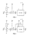
- a circuit 10 is shown that comprises a signal input 11 (IN) for receiving a digital input signal s(t), and a digital input stage 15 being designed for operation at a supply voltage V DD .
- the input stage 15 comprises several CMOS transistors and an input IINV. These transistors are sensitive to voltages across their nodes going beyond a voltage limit V max .
- voltage limiting means 14 (B) are arranged between the signal input 11 (IN) and the input IINV. The voltage limiting means 14 (B) limit the voltages at the input IINV to the supply voltage V DD .
- the voltage limiting means 14 (B) comprise an input switch (ns) being controllable by the state of the input signal s(t).
- the circuit 10 comprises means for over-voltage protection 12 (A) being situated between the signal input 11 (IN) and the supply voltage (V DD ).
- the means for over-voltage protection 12 (A) comprise at least one active circuit element being arranged so as to mimic at least the breakdown part of a zener function. I.e., the means for over-voltage protection 12 (A) at least partially operate like a zener diode.
- the circuit 10 may also comprise an input protection diode 13 (D 1 ) being situated between the input node (IN 0 ) and ground, as depicted in FIG. 4 .
- D 1 input protection diode 13
- FIG. 5 Another embodiment is illustrated in FIG. 5 .
- the circuit 20 in FIG. 5 comprises a digital input stage 25 having an input IINV and an output OUT. Like in FIG. 4 , the circuit 20 comprises means for over-voltage protection 22 (A) and voltage limiting means 24 (B).
- means 27 (D) for protection against static currents are provided.
- the means 27 (D) for protection against static currents provide for a positive feedback pulling the input IINV of the input stage 25 up to the supply voltage V DD in order to prevent static (through) currents from flowing through part of the input stage's elements.
- the means 27 (D) for protection against static currents may comprise a p-type CMOS transistor, for example.
- the circuit 20 may further comprise speed boost means 26 (C) having at least one capacitive element (Cb).
- the speed boost means 26 (C) allow the turn-on/turn-off behavior of the voltage limiting means 24 (B) to be accelerated.
- the charging of the capacitive element (Cb) depends on the state of a signal derived from the input signal s(t) such that the capacitive element (Cb) is charged to the supply voltage V DD if the input signal s(t) is low.
- the speed boost means 26 (C) together with the voltage limiting means 24 (B) may form one functional unit.
- the optional means 27 (D) for protection against static currents are employed to limit static through currents.
- Such a through current typically occurs when the voltage at the node IINV is lower than the supply voltage V DD , since the different voltages lead to a voltage difference across the digital input stage.
- FIG. 6 Yet another embodiment is depicted in FIG. 6 .
- the circuit 30 is comparable to the one depicted in FIG. 5 . Hence identical elements carry the same reference numbers as in FIG. 5 .
- the circuit 30 comprises a current limiting resistor R 1 being situated between the signal input 21 (IN) and the input node IN 0 .
- a resistor Rz is situated between the means for over-voltage protection 22 (A) and the supply voltage V DD .
- the active circuit element being part of the means for over-voltage protection (A) is a transistor.
- This transistor is arranged such that during normal operation it does not enter conductive state.
- the means for over-voltage protection (A) comprise a plurality of transistors, preferably n-channel CMOS transistors (nz 1 , nz 2 , nz 3 ), or p-channel CMOS transistors, or bipolar transistors, and a resistor Rz.
- the means (D) for protection against static currents provide for a positive feedback pulling the voltage at the input IINV up to the supply voltage V DD in order to prevent the static currents from flowing through part of the elements of the digital input stage.
- the means (D) for protection against static currents may for example comprise a p-type CMOS transistor (pp 2 ) serving as keeper transistor.
- the switch of the voltage limiting means (B) may be an n-channel CMOS transistor (ns).
- the voltage limiting means (B) may further comprise a p-channel CMOS transistor (pp 1 ) for controlling the voltage at the gate node (GNS) of the n-channel CMOS transistor (ns).
- the node GNS is a switched node.
- the means for over-voltage protection (A) may be designed so that they absorb destructive voltages when the supply voltage V DD is zero.
- FIG. 7 Another embodiment is illustrated in FIG. 7 .
- the circuit 40 comprises a digital input stage 45 with two inverters I 1 and I 2 .
- the inverter I 1 comprises a p-channel transistor pi 1 and an n-channel transistor ni 1
- the inverter I 2 comprises a p-channel transistor pi 2 and an n-channel transistor ni 2 .
- FIG. 7 further shows a proposal for elements being able to cope with high input swings using only standard elements.
- the usual protection diode D 2 to V DD is removed to avoid static current through this element.
- a bootstrap structure comprising a p-channel transistor pp 1 and a bootstrap capacitor Cb is used with the following functionality: If the input signal s(t) at node IN is low, the capacitor Cb is charged to V DD at node GNS via the p-channel transistor pp 1 and the n-channel switch transistor ns is conducting, thus transferring the input voltage at the node IN to the node IINV.
- node IN 0 goes high turning off the p-channel transistor pp 1 and the node IN 1 goes high pushing GNS high to keep the n-channel switch transistor ns in conduction.
- the input state at IN is transferred to the node IINV, but limited in swing by the n-channel switch transistor ns.
- Any excessive voltage at the node GNS is discharged via the p-channel transistor pp 1 to V DD by the p-channel transistor pp 1 going into reverse conduction. In this way, the voltage at the node GNS is limited to one p-channel transistor threshold voltage above V DD .
- a keeper transistor pp 2 which also limits the voltage at the node IINV to V DD .
- a resistor R 2 may be employed that slightly delays the input signal at the node IN 1 .
- the sequence at the input IN starts with a high voltage after power-up, the sequence starts with the first falling edge on IN.
- the circuit 40 shall also be operating with a standard input swing between 0 and V DD .
- the means for over-voltage protection 22 (A) may be comprised of any combination of n-channel, p-channel or bipolar diodes.
- the signal at the node GNS almost follows the signal s(t). It shows a peak at the falling edge of the signal s(t) that almost goes back to 0 Volt.
- the circuit blocks A, B, C, and D provide for a voltage x(t) at the node IINV that closely follows the signal s(t) at the input IN.
- the edges are somewhat rounded.
- the signal at the node GNS slowly builds up before it more or less follows the signal s(t).
- the circuit blocks A, B, C, and D provide for a voltage x(t) at the node IINV that after some delay (in the present example the delay is about 250 ns, but only for the first pulse after power-up) closely follows the signal s(t) at the input IN.
- the edges are somewhat rounded.
- the signal y(t) is also delayed.
- FIGS. 10 and 11 are given to illustrate that the whole circuit 40 is also fully functional when the signal swing of the signal s(t) is low.
- the signal swing of s(t) remains below 1 Volt.
- protection element (A) which absorbs destructive voltages, when the supply voltage is turned off.
- CMOS complementary metal oxide semiconductor
- BiCMOS circuits bipolar devices combined with CMOS subcircuits on a single chip
Landscapes
- Physics & Mathematics (AREA)
- Engineering & Computer Science (AREA)
- Computer Hardware Design (AREA)
- Computing Systems (AREA)
- General Engineering & Computer Science (AREA)
- Mathematical Physics (AREA)
- Logic Circuits (AREA)
- Semiconductor Integrated Circuits (AREA)
- Amplifiers (AREA)
- Emergency Protection Circuit Devices (AREA)
- Metal-Oxide And Bipolar Metal-Oxide Semiconductor Integrated Circuits (AREA)
Abstract
Description
-
- an additional high voltage supply domain,
- a level shifter to bridge the two supply domains,
- additional fabrication process steps, to provide transistors, which withstand high voltages.
Claims (13)
Applications Claiming Priority (3)
| Application Number | Priority Date | Filing Date | Title |
|---|---|---|---|
| EP02002681.1 | 2002-02-06 | ||
| EP02002681 | 2002-02-06 | ||
| PCT/IB2003/000298 WO2003067761A1 (en) | 2002-02-06 | 2003-01-29 | Input stage resistant against high voltage swings |
Publications (2)
| Publication Number | Publication Date |
|---|---|
| US20050088208A1 US20050088208A1 (en) | 2005-04-28 |
| US7135908B2 true US7135908B2 (en) | 2006-11-14 |
Family
ID=27675604
Family Applications (1)
| Application Number | Title | Priority Date | Filing Date |
|---|---|---|---|
| US10/503,428 Expired - Fee Related US7135908B2 (en) | 2002-02-06 | 2003-01-29 | Input stage resistant against high voltage swings |
Country Status (8)
| Country | Link |
|---|---|
| US (1) | US7135908B2 (en) |
| EP (1) | EP1474870B1 (en) |
| JP (1) | JP2006500795A (en) |
| CN (1) | CN100379152C (en) |
| AT (1) | ATE396540T1 (en) |
| AU (1) | AU2003244420A1 (en) |
| DE (1) | DE60321135D1 (en) |
| WO (1) | WO2003067761A1 (en) |
Cited By (1)
| Publication number | Priority date | Publication date | Assignee | Title |
|---|---|---|---|---|
| US20090267584A1 (en) * | 2008-04-23 | 2009-10-29 | Himax Technologies Limited | Transient detection circuit |
Families Citing this family (3)
| Publication number | Priority date | Publication date | Assignee | Title |
|---|---|---|---|---|
| EP1768240A4 (en) * | 2004-06-09 | 2008-05-28 | Rohm Co Ltd | Level shift circuit and switching regulator using the same |
| JP2006294903A (en) * | 2005-04-12 | 2006-10-26 | Nec Electronics Corp | Fuse trimming circuit |
| CN111276956B (en) * | 2020-02-14 | 2022-05-31 | 西安微电子技术研究所 | Bipolar rail-to-rail operational amplifier input end general electrostatic protection circuit |
Citations (4)
| Publication number | Priority date | Publication date | Assignee | Title |
|---|---|---|---|---|
| US4858055A (en) * | 1987-07-23 | 1989-08-15 | Mitsubishi Denki Kabushiki Kaisha | Input protecting device for a semiconductor circuit device |
| US5574395A (en) * | 1994-06-17 | 1996-11-12 | Mitsubishi Denki Kabushiki Kaisha | Semiconductor circuit |
| US6181193B1 (en) * | 1999-10-08 | 2001-01-30 | International Business Machines Corporation | Using thick-oxide CMOS devices to interface high voltage integrated circuits |
| US6291288B1 (en) * | 1999-04-15 | 2001-09-18 | United Microelectronics Corp. | Method of fabricating a thin and structurally-undefective dielectric structure for a storage capacitor in dynamic random-access memory |
Family Cites Families (1)
| Publication number | Priority date | Publication date | Assignee | Title |
|---|---|---|---|---|
| US5852540A (en) * | 1997-09-24 | 1998-12-22 | Intel Corporation | Circuit for protecting the input/output stage of a low voltage integrated circuit device from a failure of the internal voltage supply or a difference in the power-up sequencing of supply voltage levels |
-
2003
- 2003-01-29 US US10/503,428 patent/US7135908B2/en not_active Expired - Fee Related
- 2003-01-29 WO PCT/IB2003/000298 patent/WO2003067761A1/en not_active Ceased
- 2003-01-29 AU AU2003244420A patent/AU2003244420A1/en not_active Abandoned
- 2003-01-29 AT AT03737407T patent/ATE396540T1/en not_active IP Right Cessation
- 2003-01-29 EP EP03737407A patent/EP1474870B1/en not_active Expired - Lifetime
- 2003-01-29 DE DE60321135T patent/DE60321135D1/en not_active Expired - Lifetime
- 2003-01-29 JP JP2003566984A patent/JP2006500795A/en active Pending
- 2003-01-29 CN CNB038032295A patent/CN100379152C/en not_active Expired - Fee Related
Patent Citations (4)
| Publication number | Priority date | Publication date | Assignee | Title |
|---|---|---|---|---|
| US4858055A (en) * | 1987-07-23 | 1989-08-15 | Mitsubishi Denki Kabushiki Kaisha | Input protecting device for a semiconductor circuit device |
| US5574395A (en) * | 1994-06-17 | 1996-11-12 | Mitsubishi Denki Kabushiki Kaisha | Semiconductor circuit |
| US6291288B1 (en) * | 1999-04-15 | 2001-09-18 | United Microelectronics Corp. | Method of fabricating a thin and structurally-undefective dielectric structure for a storage capacitor in dynamic random-access memory |
| US6181193B1 (en) * | 1999-10-08 | 2001-01-30 | International Business Machines Corporation | Using thick-oxide CMOS devices to interface high voltage integrated circuits |
Non-Patent Citations (2)
| Title |
|---|
| "Overvoltage Protection Circuit", IBM Technical Disclosure Bulletin, vol. 30, No. 12, May 1, 1988, pp. 96-97. |
| NN880596, "Overvoltage Protection Circuit", IBM Technical Disclosure Bulletin, IBM Corp., US, vol. 30, No. 12, May 1988, p. 96-97. * |
Cited By (2)
| Publication number | Priority date | Publication date | Assignee | Title |
|---|---|---|---|---|
| US20090267584A1 (en) * | 2008-04-23 | 2009-10-29 | Himax Technologies Limited | Transient detection circuit |
| US7826187B2 (en) * | 2008-04-23 | 2010-11-02 | Himax Technologies Limited | Transient detection circuit |
Also Published As
| Publication number | Publication date |
|---|---|
| CN100379152C (en) | 2008-04-02 |
| CN1628416A (en) | 2005-06-15 |
| DE60321135D1 (en) | 2008-07-03 |
| EP1474870B1 (en) | 2008-05-21 |
| JP2006500795A (en) | 2006-01-05 |
| ATE396540T1 (en) | 2008-06-15 |
| EP1474870A1 (en) | 2004-11-10 |
| US20050088208A1 (en) | 2005-04-28 |
| AU2003244420A1 (en) | 2003-09-02 |
| WO2003067761A1 (en) | 2003-08-14 |
Similar Documents
| Publication | Publication Date | Title |
|---|---|---|
| EP0643487B1 (en) | MOS output circuit with leakage current protection | |
| US6744291B2 (en) | Power-on reset circuit | |
| US5576635A (en) | Output buffer with improved tolerance to overvoltage | |
| US7221551B2 (en) | Cascaded gate-driven ESD clamp | |
| KR100968647B1 (en) | ESD protection circuit | |
| US6008970A (en) | Power supply clamp circuitry for electrostatic discharge (ESD) protection | |
| JPH077411A (en) | Overvoltage-allowable output buffer circuit | |
| JPH11274911A (en) | Output buffer with voltage withstanding characteristic | |
| US7394638B2 (en) | System and method for a whole-chip electrostatic discharge protection that is independent of relative supply rail voltages and supply sequencing | |
| KR20060049381A (en) | Integrated circuit comprising an ESD prevention circuit and at least one ESD prevention circuit | |
| US7138836B2 (en) | Hot carrier injection suppression circuit | |
| US6294943B1 (en) | Method of designing fail-safe CMOS I/O buffers whose external nodes accept voltages higher than the maximum gate oxide operating voltage | |
| US7135908B2 (en) | Input stage resistant against high voltage swings | |
| US6388855B1 (en) | Transistor protecting circuit with enhancing circuit for H bridge circuit | |
| EP0840453A2 (en) | An output buffer | |
| US7123059B2 (en) | Output stage resistant against high voltage swings | |
| US20080165459A1 (en) | Pad ESD Spreading Technique | |
| KR20080066969A (en) | High Voltage Tolerant Port Driver | |
| JPH0212867A (en) | Semiconductor integrated circuit | |
| EP1461861B1 (en) | Method and circuit for suppressing hot carrier injection | |
| US7514951B2 (en) | Negative voltage noise-free circuit for multi-functional pad | |
| KR100212146B1 (en) | Protection circuit of isolated circuit at the power supply end | |
| KR19980028053A (en) | Output buffer circuit of semiconductor memory device |
Legal Events
| Date | Code | Title | Description |
|---|---|---|---|
| AS | Assignment |
Owner name: KONINKLIJKE PHILIPS ELECTRONICS N.V., NETHERLANDS Free format text: ASSIGNMENT OF ASSIGNORS INTEREST;ASSIGNOR:BECKER, ROLF;REEL/FRAME:016114/0223 Effective date: 20030210 |
|
| AS | Assignment |
Owner name: NXP B.V., NETHERLANDS Free format text: ASSIGNMENT OF ASSIGNORS INTEREST;ASSIGNOR:KONINKLIJKE PHILIPS ELECTRONICS N.V.;REEL/FRAME:019719/0843 Effective date: 20070704 Owner name: NXP B.V.,NETHERLANDS Free format text: ASSIGNMENT OF ASSIGNORS INTEREST;ASSIGNOR:KONINKLIJKE PHILIPS ELECTRONICS N.V.;REEL/FRAME:019719/0843 Effective date: 20070704 |
|
| FEPP | Fee payment procedure |
Free format text: PAYOR NUMBER ASSIGNED (ORIGINAL EVENT CODE: ASPN); ENTITY STATUS OF PATENT OWNER: LARGE ENTITY |
|
| FPAY | Fee payment |
Year of fee payment: 4 |
|
| FPAY | Fee payment |
Year of fee payment: 8 |
|
| AS | Assignment |
Owner name: ST WIRELESS SA, SWITZERLAND Free format text: ASSIGNMENT OF ASSIGNORS INTEREST;ASSIGNOR:NXP B.V.;REEL/FRAME:037624/0831 Effective date: 20080728 |
|
| AS | Assignment |
Owner name: ST-ERICSSON SA, SWITZERLAND Free format text: CHANGE OF NAME;ASSIGNOR:ST WIRELESS SA;REEL/FRAME:037683/0128 Effective date: 20080714 Owner name: ST-ERICSSON SA, EN LIQUIDATION, SWITZERLAND Free format text: STATUS CHANGE-ENTITY IN LIQUIDATION;ASSIGNOR:ST-ERICSSON SA;REEL/FRAME:037739/0493 Effective date: 20150223 |
|
| FEPP | Fee payment procedure |
Free format text: MAINTENANCE FEE REMINDER MAILED (ORIGINAL EVENT CODE: REM.) |
|
| LAPS | Lapse for failure to pay maintenance fees |
Free format text: PATENT EXPIRED FOR FAILURE TO PAY MAINTENANCE FEES (ORIGINAL EVENT CODE: EXP.); ENTITY STATUS OF PATENT OWNER: LARGE ENTITY |
|
| STCH | Information on status: patent discontinuation |
Free format text: PATENT EXPIRED DUE TO NONPAYMENT OF MAINTENANCE FEES UNDER 37 CFR 1.362 |
|
| FP | Lapsed due to failure to pay maintenance fee |
Effective date: 20181114 |