US7078821B2 - Ball film for integrated circuit fabrication and testing - Google Patents
Ball film for integrated circuit fabrication and testing Download PDFInfo
- Publication number
- US7078821B2 US7078821B2 US10/648,963 US64896303A US7078821B2 US 7078821 B2 US7078821 B2 US 7078821B2 US 64896303 A US64896303 A US 64896303A US 7078821 B2 US7078821 B2 US 7078821B2
- Authority
- US
- United States
- Prior art keywords
- ball
- film
- thin film
- metal balls
- balls
- Prior art date
- Legal status (The legal status is an assumption and is not a legal conclusion. Google has not performed a legal analysis and makes no representation as to the accuracy of the status listed.)
- Expired - Lifetime, expires
Links
- 238000004519 manufacturing process Methods 0.000 title abstract description 6
- 239000002184 metal Substances 0.000 claims abstract description 55
- 229910052751 metal Inorganic materials 0.000 claims abstract description 55
- 239000010408 film Substances 0.000 claims abstract description 41
- 239000010409 thin film Substances 0.000 claims abstract description 31
- 229910000679 solder Inorganic materials 0.000 claims description 28
- 239000004642 Polyimide Substances 0.000 claims description 2
- 229920001721 polyimide Polymers 0.000 claims description 2
- 239000000758 substrate Substances 0.000 abstract description 11
- 238000010168 coupling process Methods 0.000 abstract description 8
- 230000008878 coupling Effects 0.000 abstract description 7
- 238000005859 coupling reaction Methods 0.000 abstract description 7
- 238000000034 method Methods 0.000 description 19
- PCHJSUWPFVWCPO-UHFFFAOYSA-N gold Chemical compound [Au] PCHJSUWPFVWCPO-UHFFFAOYSA-N 0.000 description 8
- 229910052737 gold Inorganic materials 0.000 description 8
- 239000010931 gold Substances 0.000 description 8
- 230000008569 process Effects 0.000 description 4
- 239000000463 material Substances 0.000 description 3
- 239000004020 conductor Substances 0.000 description 2
- 238000004806 packaging method and process Methods 0.000 description 2
- 238000010998 test method Methods 0.000 description 2
- 238000007792 addition Methods 0.000 description 1
- 230000004075 alteration Effects 0.000 description 1
- 238000003491 array Methods 0.000 description 1
- 230000002860 competitive effect Effects 0.000 description 1
- 238000005516 engineering process Methods 0.000 description 1
- 230000005496 eutectics Effects 0.000 description 1
- 239000011368 organic material Substances 0.000 description 1
- 239000004065 semiconductor Substances 0.000 description 1
- 238000012956 testing procedure Methods 0.000 description 1
Images


Classifications
-
- G—PHYSICS
- G01—MEASURING; TESTING
- G01R—MEASURING ELECTRIC VARIABLES; MEASURING MAGNETIC VARIABLES
- G01R1/00—Details of instruments or arrangements of the types included in groups G01R5/00 - G01R13/00 and G01R31/00
- G01R1/02—General constructional details
- G01R1/06—Measuring leads; Measuring probes
- G01R1/067—Measuring probes
- G01R1/073—Multiple probes
- G01R1/07307—Multiple probes with individual probe elements, e.g. needles, cantilever beams or bump contacts, fixed in relation to each other, e.g. bed of nails fixture or probe card
- G01R1/0735—Multiple probes with individual probe elements, e.g. needles, cantilever beams or bump contacts, fixed in relation to each other, e.g. bed of nails fixture or probe card arranged on a flexible frame or film
-
- H—ELECTRICITY
- H01—ELECTRIC ELEMENTS
- H01L—SEMICONDUCTOR DEVICES NOT COVERED BY CLASS H10
- H01L21/00—Processes or apparatus adapted for the manufacture or treatment of semiconductor or solid state devices or of parts thereof
- H01L21/02—Manufacture or treatment of semiconductor devices or of parts thereof
- H01L21/04—Manufacture or treatment of semiconductor devices or of parts thereof the devices having potential barriers, e.g. a PN junction, depletion layer or carrier concentration layer
- H01L21/48—Manufacture or treatment of parts, e.g. containers, prior to assembly of the devices, using processes not provided for in a single one of the subgroups H01L21/06 - H01L21/326
- H01L21/4814—Conductive parts
- H01L21/4846—Leads on or in insulating or insulated substrates, e.g. metallisation
- H01L21/4853—Connection or disconnection of other leads to or from a metallisation, e.g. pins, wires, bumps
-
- H—ELECTRICITY
- H01—ELECTRIC ELEMENTS
- H01L—SEMICONDUCTOR DEVICES NOT COVERED BY CLASS H10
- H01L24/00—Arrangements for connecting or disconnecting semiconductor or solid-state bodies; Methods or apparatus related thereto
- H01L24/01—Means for bonding being attached to, or being formed on, the surface to be connected, e.g. chip-to-package, die-attach, "first-level" interconnects; Manufacturing methods related thereto
- H01L24/10—Bump connectors ; Manufacturing methods related thereto
- H01L24/11—Manufacturing methods
-
- H—ELECTRICITY
- H05—ELECTRIC TECHNIQUES NOT OTHERWISE PROVIDED FOR
- H05K—PRINTED CIRCUITS; CASINGS OR CONSTRUCTIONAL DETAILS OF ELECTRIC APPARATUS; MANUFACTURE OF ASSEMBLAGES OF ELECTRICAL COMPONENTS
- H05K3/00—Apparatus or processes for manufacturing printed circuits
- H05K3/30—Assembling printed circuits with electric components, e.g. with resistor
- H05K3/32—Assembling printed circuits with electric components, e.g. with resistor electrically connecting electric components or wires to printed circuits
- H05K3/34—Assembling printed circuits with electric components, e.g. with resistor electrically connecting electric components or wires to printed circuits by soldering
- H05K3/3457—Solder materials or compositions; Methods of application thereof
- H05K3/3478—Applying solder preforms; Transferring prefabricated solder patterns
-
- H—ELECTRICITY
- H01—ELECTRIC ELEMENTS
- H01L—SEMICONDUCTOR DEVICES NOT COVERED BY CLASS H10
- H01L2224/00—Indexing scheme for arrangements for connecting or disconnecting semiconductor or solid-state bodies and methods related thereto as covered by H01L24/00
- H01L2224/01—Means for bonding being attached to, or being formed on, the surface to be connected, e.g. chip-to-package, die-attach, "first-level" interconnects; Manufacturing methods related thereto
- H01L2224/02—Bonding areas; Manufacturing methods related thereto
- H01L2224/04—Structure, shape, material or disposition of the bonding areas prior to the connecting process
- H01L2224/05—Structure, shape, material or disposition of the bonding areas prior to the connecting process of an individual bonding area
- H01L2224/0554—External layer
- H01L2224/0556—Disposition
- H01L2224/05571—Disposition the external layer being disposed in a recess of the surface
-
- H—ELECTRICITY
- H01—ELECTRIC ELEMENTS
- H01L—SEMICONDUCTOR DEVICES NOT COVERED BY CLASS H10
- H01L2224/00—Indexing scheme for arrangements for connecting or disconnecting semiconductor or solid-state bodies and methods related thereto as covered by H01L24/00
- H01L2224/01—Means for bonding being attached to, or being formed on, the surface to be connected, e.g. chip-to-package, die-attach, "first-level" interconnects; Manufacturing methods related thereto
- H01L2224/02—Bonding areas; Manufacturing methods related thereto
- H01L2224/04—Structure, shape, material or disposition of the bonding areas prior to the connecting process
- H01L2224/05—Structure, shape, material or disposition of the bonding areas prior to the connecting process of an individual bonding area
- H01L2224/0554—External layer
- H01L2224/05573—Single external layer
-
- H—ELECTRICITY
- H01—ELECTRIC ELEMENTS
- H01L—SEMICONDUCTOR DEVICES NOT COVERED BY CLASS H10
- H01L2224/00—Indexing scheme for arrangements for connecting or disconnecting semiconductor or solid-state bodies and methods related thereto as covered by H01L24/00
- H01L2224/01—Means for bonding being attached to, or being formed on, the surface to be connected, e.g. chip-to-package, die-attach, "first-level" interconnects; Manufacturing methods related thereto
- H01L2224/10—Bump connectors; Manufacturing methods related thereto
- H01L2224/12—Structure, shape, material or disposition of the bump connectors prior to the connecting process
- H01L2224/13—Structure, shape, material or disposition of the bump connectors prior to the connecting process of an individual bump connector
- H01L2224/13001—Core members of the bump connector
- H01L2224/13099—Material
-
- H—ELECTRICITY
- H01—ELECTRIC ELEMENTS
- H01L—SEMICONDUCTOR DEVICES NOT COVERED BY CLASS H10
- H01L2924/00—Indexing scheme for arrangements or methods for connecting or disconnecting semiconductor or solid-state bodies as covered by H01L24/00
- H01L2924/0001—Technical content checked by a classifier
- H01L2924/00014—Technical content checked by a classifier the subject-matter covered by the group, the symbol of which is combined with the symbol of this group, being disclosed without further technical details
-
- H—ELECTRICITY
- H01—ELECTRIC ELEMENTS
- H01L—SEMICONDUCTOR DEVICES NOT COVERED BY CLASS H10
- H01L2924/00—Indexing scheme for arrangements or methods for connecting or disconnecting semiconductor or solid-state bodies as covered by H01L24/00
- H01L2924/0001—Technical content checked by a classifier
- H01L2924/00015—Technical content checked by a classifier the subject-matter covered by the group, the symbol of which is combined with the symbol of this group, being disclosed as prior art
-
- H—ELECTRICITY
- H01—ELECTRIC ELEMENTS
- H01L—SEMICONDUCTOR DEVICES NOT COVERED BY CLASS H10
- H01L2924/00—Indexing scheme for arrangements or methods for connecting or disconnecting semiconductor or solid-state bodies as covered by H01L24/00
- H01L2924/01—Chemical elements
- H01L2924/01005—Boron [B]
-
- H—ELECTRICITY
- H01—ELECTRIC ELEMENTS
- H01L—SEMICONDUCTOR DEVICES NOT COVERED BY CLASS H10
- H01L2924/00—Indexing scheme for arrangements or methods for connecting or disconnecting semiconductor or solid-state bodies as covered by H01L24/00
- H01L2924/01—Chemical elements
- H01L2924/01033—Arsenic [As]
-
- H—ELECTRICITY
- H01—ELECTRIC ELEMENTS
- H01L—SEMICONDUCTOR DEVICES NOT COVERED BY CLASS H10
- H01L2924/00—Indexing scheme for arrangements or methods for connecting or disconnecting semiconductor or solid-state bodies as covered by H01L24/00
- H01L2924/01—Chemical elements
- H01L2924/01079—Gold [Au]
-
- H—ELECTRICITY
- H01—ELECTRIC ELEMENTS
- H01L—SEMICONDUCTOR DEVICES NOT COVERED BY CLASS H10
- H01L2924/00—Indexing scheme for arrangements or methods for connecting or disconnecting semiconductor or solid-state bodies as covered by H01L24/00
- H01L2924/01—Chemical elements
- H01L2924/01082—Lead [Pb]
-
- H—ELECTRICITY
- H01—ELECTRIC ELEMENTS
- H01L—SEMICONDUCTOR DEVICES NOT COVERED BY CLASS H10
- H01L2924/00—Indexing scheme for arrangements or methods for connecting or disconnecting semiconductor or solid-state bodies as covered by H01L24/00
- H01L2924/013—Alloys
- H01L2924/0132—Binary Alloys
- H01L2924/01322—Eutectic Alloys, i.e. obtained by a liquid transforming into two solid phases
-
- H—ELECTRICITY
- H01—ELECTRIC ELEMENTS
- H01L—SEMICONDUCTOR DEVICES NOT COVERED BY CLASS H10
- H01L2924/00—Indexing scheme for arrangements or methods for connecting or disconnecting semiconductor or solid-state bodies as covered by H01L24/00
- H01L2924/013—Alloys
- H01L2924/014—Solder alloys
-
- H—ELECTRICITY
- H01—ELECTRIC ELEMENTS
- H01L—SEMICONDUCTOR DEVICES NOT COVERED BY CLASS H10
- H01L2924/00—Indexing scheme for arrangements or methods for connecting or disconnecting semiconductor or solid-state bodies as covered by H01L24/00
- H01L2924/10—Details of semiconductor or other solid state devices to be connected
- H01L2924/11—Device type
- H01L2924/14—Integrated circuits
-
- H—ELECTRICITY
- H05—ELECTRIC TECHNIQUES NOT OTHERWISE PROVIDED FOR
- H05K—PRINTED CIRCUITS; CASINGS OR CONSTRUCTIONAL DETAILS OF ELECTRIC APPARATUS; MANUFACTURE OF ASSEMBLAGES OF ELECTRICAL COMPONENTS
- H05K2201/00—Indexing scheme relating to printed circuits covered by H05K1/00
- H05K2201/10—Details of components or other objects attached to or integrated in a printed circuit board
- H05K2201/10227—Other objects, e.g. metallic pieces
- H05K2201/10424—Frame holders
-
- H—ELECTRICITY
- H05—ELECTRIC TECHNIQUES NOT OTHERWISE PROVIDED FOR
- H05K—PRINTED CIRCUITS; CASINGS OR CONSTRUCTIONAL DETAILS OF ELECTRIC APPARATUS; MANUFACTURE OF ASSEMBLAGES OF ELECTRICAL COMPONENTS
- H05K2203/00—Indexing scheme relating to apparatus or processes for manufacturing printed circuits covered by H05K3/00
- H05K2203/03—Metal processing
- H05K2203/0338—Transferring metal or conductive material other than a circuit pattern, e.g. bump, solder, printed component
-
- H—ELECTRICITY
- H05—ELECTRIC TECHNIQUES NOT OTHERWISE PROVIDED FOR
- H05K—PRINTED CIRCUITS; CASINGS OR CONSTRUCTIONAL DETAILS OF ELECTRIC APPARATUS; MANUFACTURE OF ASSEMBLAGES OF ELECTRICAL COMPONENTS
- H05K2203/00—Indexing scheme relating to apparatus or processes for manufacturing printed circuits covered by H05K3/00
- H05K2203/04—Soldering or other types of metallurgic bonding
- H05K2203/041—Solder preforms in the shape of solder balls
Definitions
- This invention relates generally to the field of integrated circuit packaging and, more specifically, to a ball film for integrated circuit fabrication and testing.
- Integrated circuit packages such as ball grid arrays
- solder balls may become damaged when testing due to current testing procedures.
- attachment of solder balls or bumps as they are sometimes referred to are important in keeping costs down and quality and realiability up.
- a method of fabricating ball grid array packages includes providing a substrate, providing a ball film that includes a plurality of metal balls movably contained within respective slots of a thin film, coupling the metal balls to the substrate, and removing the thin film from the metal balls.
- a ball film manufactured according to the teachings of the invention may be utilized as a buffer between the solder balls of a ball grid array package and the metal contact pins of a socket during testing in order to prevent damage to the solder balls.
- a ball film may be utilized to attach solder balls to a ball grid array package substrate. This eliminates the need for a vacuum pick operation as well as increasing the quality of the solder ball attach process.
- a ball film may be utilized to attach gold or solder balls to bond pads on an integrated circuit chip. By using the layout of the chip mask pattern, the process may be highly accurate. This eliminates the need for mechanical wire bump operation.
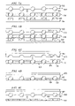
- FIGS. 1A and 1B are plan and cross-sectional elevation views, respectively, of a ball film in accordance with an embodiment of the invention
- FIGS. 2A through 2C are a series of cross-sectional elevation views illustrating a method of forming the ball film of FIGS. 1A and 1B in accordance with an embodiment of the invention
- FIGS. 3A and 3B are elevation views illustrating a method of testing a ball grid array package utilizing a ball film in accordance with an embodiment of the invention
- FIGS. 4A through 4C are elevation views illustrating a method of coupling solder balls to a ball grid array package substrate utilizing a ball film in accordance with an embodiment of the invention.
- FIGS. 5A through 5C are elevation views illustrating a method of coupling gold balls to a integrated circuit chip utilizing a ball film in accordance with an embodiment of the invention.
- FIGS. 1A through 5C of the drawings in which like numerals refer to like parts.
- FIGS. 1A and 1B are plan and cross-sectional elevation views, respectively, of a ball film 100 in accordance with an embodiment of the invention.
- ball film 100 includes a plurality of metal balls 102 movably contained within respective slots 103 of a thin film 104 .
- Ball film 100 may have any suitable size and shape and may have any suitable pattern of metal balls 102 .
- metal balls 102 may be in the form of an array or may be randomly positioned.
- a method of forming ball film 100 is described in greater detail below in conjunction with FIGS. 2A through 2C and various functions of ball film 100 are described below in conjunction with FIGS. 3A and 3B , 4 A through 4 C, and 5 A through 5 C.
- Metal balls 102 may be formed from any suitable conductive material.
- metal balls 102 may be formed from eutectic solder, lead-free solder, gold, or other suitable conductive material.
- metal balls 102 may have any suitable size and shape, it is preferable that metal balls 102 be formed in a spherical shape with each metal ball 102 having a diameter of between 0.1 mm and 0.5 mm, depending on the application for ball film 100 . Any suitable fabrication method may be utilized to form metal balls 102 , such as micro machine technology.
- a pitch between the centerlines of metal balls 102 may be any suitable length; however, in one embodiment, the pitch between centerlines of metal balls 102 is between approximately 0.15 mm and 0.65 mm.
- Thin film 104 may be any suitable size and shape and may be formed from any suitable material. In one embodiment, thin film 104 has a thickness of between 0.01 mm and 0.4 mm; however, other suitable thickness are contemplated by the present invention. In addition, thin film 104 may be formed from polyimide, a suitable organic material, and the like. Thin film 104 may also be formed from any suitable number of layers having the same or different material type. As described above, slots 103 are formed in thin film 104 in order to movably contain metal balls 102 therein. Although slots 103 may have any suitable shape, it is preferable that slots 103 have a spherical shape.
- slots 103 have a spherical shape that corresponds to a spherical shape of metal balls 102 .
- a radius of the spherical slots is larger than the radius of metal balls 102 to facilitate the movable nature of metal balls 102 within slots 103 . This results in a gap 107 on either side of metal balls 102 to facilitate translational movement of metal balls 102 in addition to rotational movement of metal balls 102 .
- the reasons for having metal balls 102 movably contained within slots 103 is described in further detail below.
- FIGS. 2A through 2C are a series of cross-sectional elevation views illustrating an example method of forming ball film 100 in accordance with an embodiment of the invention.
- a first thin film 106 is illustrated.
- First thin film 106 forms one half of thin film 104 (the “lower” half in the illustrated example).
- First thin film 106 has a first slot 108 formed therein.
- first slot 108 may have any suitable shape, in the illustrated embodiment, first slot 108 is spherically shaped with a wall having a particular radius 109 .
- a metal ball 102 within first slot 108 is illustrated. Any suitable method may be used to position metal ball 102 within first slot 108 . As illustrated in FIG. 2B , a radius 110 of metal ball 102 is smaller than radius 109 of first slot 108 .
- Second thin film 111 includes a second slot 112 that corresponds to first slot 108 in such a manner as to form slot 103 of thin film 104 .
- second slot 112 is spherically shaped and is essentially a mirror image of first slot 108 in order to form spherically shaped slot 103 .
- second slot 112 has a radius 113 substantially equal to radius 109 of first slot 108 . This facilitates gap 107 , as described above.
- metal ball 102 is both translationally and rotatably contained within slot 103 . This ends the example method as outlined in FIGS. 2A through 2C .
- ball film 100 may be utilized in many different applications. Three such applications are described below in conjunction with FIGS. 3A and 3B , 4 A through 4 C, and 5 A through 5 C.
- FIGS. 3A and 3B are elevation views illustrating a method of testing a ball grid array package 300 utilizing ball film 100 in accordance with an embodiment of the invention.
- ball grid array package 300 includes a substrate 302 having a plurality of solder balls 304 coupled thereto.
- Ball grid array package 300 is to be tested with a contact board 306 having a plurality of metal contact pins 308 .
- Metal contact pins 308 are typically arranged in a pattern that matches a pattern of solder balls 304 .
- the solder balls of the ball grid array package directly contact the metal contact pins of the contact board during testing.
- ball film 100 is positioned between ball grid array package 300 and contact board 306 in such a manner that each metal ball 102 of ball film 100 is positioned between a respective solder ball 304 and a respective metal contact pin 308 to act as a buffer. Because of the movable nature of metal balls 102 within slots 103 of thin film 104 , pressure exerted against solder balls 304 of ball grid array package 300 is alleviated and the potential of damaging the solder balls 304 is substantially reduced or eliminated. Any damage that may occur is received by metal balls 102 of ball film 100 .
- FIGS. 4A through 4C are elevation views illustrating a method of coupling solder balls to a ball grid array package 400 utilizing ball film 100 in accordance with an embodiment of the invention.
- ball grid array package 400 includes a substrate 402 having a plurality of slots 404 formed therein.
- slots 404 may have any suitable size and shape, it is preferable that the size and shape of slots 404 match up with the size and shape of metal balls 102 of ball film 100 .
- the pattern of slots 404 should be arranged in such a manner that it matches the pattern of metal balls 102 of ball film 100 .
- ball film 100 is engaged in substrate 402 of ball grid array package 400 such that metal balls 102 are coupled to slots 404 . Any suitable coupling method may be utilized. Metal balls 102 will become the solder balls for ball grid array package 400 . Accordingly, referring to FIG. 4C , in order to complete the attachment of the solder balls to ball grid array package 400 , thin film 104 of ball film 100 is removed from metal balls 102 , while keeping metal balls 102 coupled to substrate 402 of ball grid array package 400 . Any suitable removal method may be utilized to remove thin film 104 .
- FIGS. 5A through 5C are elevation views illustrating a method of coupling gold bumps to an integrated circuit chip 500 utilizing ball film 100 in accordance with an embodiment of the invention.
- Integrated circuit chip 500 includes a plurality of bond pads 502 formed from any suitable material and arranged in any suitable pattern. In this example, it is desired to attach gold bumps to bond pads 502 . This may be done using ball film 100 having metal balls 102 that are formed from gold. The pattern of metal balls 102 substantially match the pattern of bond pads 502 on integrated circuit chip 500 . The pattern for metal balls 102 may be based upon the chip mask for integrated circuit chip 500 in order to get an accurate pattern.
- metal balls 102 are illustrated as being coupled to bond pads 502 . This may be accomplished using any suitable method.
- thin film 104 is removed from metal balls 102 , as illustrated in FIG. 5C . Any suitable removal method may be utilized to remove thin film 104 .
- ball film 100 manufactured according to the teachings of the invention may be utilized in many different applications, such as a buffer between the solder balls of a ball grid array package and the metal contact pins of a socket during testing in order to prevent damage to the solder balls, as well as to attach solder balls to a ball grid array package substrate.
- Ball film 100 may be utilized to attach gold or solder bumps to bond pads on an integrated circuit chip. By using the layout of the chip mask pattern, the process may be highly accurate. This eliminates the need for mechanical wire bump operation. Other suitable applications are contemplated by the present invention.
Landscapes
- Engineering & Computer Science (AREA)
- Manufacturing & Machinery (AREA)
- Microelectronics & Electronic Packaging (AREA)
- Physics & Mathematics (AREA)
- General Physics & Mathematics (AREA)
- Computer Hardware Design (AREA)
- Power Engineering (AREA)
- Ceramic Engineering (AREA)
- Condensed Matter Physics & Semiconductors (AREA)
- Electric Connection Of Electric Components To Printed Circuits (AREA)
- Testing Of Individual Semiconductor Devices (AREA)
- Testing Or Measuring Of Semiconductors Or The Like (AREA)
Abstract
According to one embodiment of the invention, a method of fabricating ball grid array packages includes providing a substrate, providing a ball film that includes a plurality of metal balls movably contained within respective slots of a thin film, coupling the metal balls to the substrate, and removing the thin film from the metal balls.
Description
This invention relates generally to the field of integrated circuit packaging and, more specifically, to a ball film for integrated circuit fabrication and testing.
Because of the sheer volume of integrated circuits in the marketplace, packaging of integrated circuits and testing of the completed packages in a cost-effective manner is important for semiconductor manufacturers in order that they can be competitive in the marketplace. Integrated circuit packages, such as ball grid arrays, can be tricky to manufacture efficiently and the solder balls may become damaged when testing due to current testing procedures. In addition, the attachment of solder balls or bumps as they are sometimes referred to are important in keeping costs down and quality and realiability up.
According to one embodiment of the invention, a method of fabricating ball grid array packages includes providing a substrate, providing a ball film that includes a plurality of metal balls movably contained within respective slots of a thin film, coupling the metal balls to the substrate, and removing the thin film from the metal balls.
Some embodiments of the invention provide numerous technical advantages. Other embodiments may realize some, none, or all of these advantages. For example, a ball film manufactured according to the teachings of the invention may be utilized as a buffer between the solder balls of a ball grid array package and the metal contact pins of a socket during testing in order to prevent damage to the solder balls. In addition, because the balls in the ball film can freely rotate, improved contact between all solder balls and their respective contact pins is improved. In another example, a ball film may be utilized to attach solder balls to a ball grid array package substrate. This eliminates the need for a vacuum pick operation as well as increasing the quality of the solder ball attach process. In another example, a ball film may be utilized to attach gold or solder balls to bond pads on an integrated circuit chip. By using the layout of the chip mask pattern, the process may be highly accurate. This eliminates the need for mechanical wire bump operation.
Other technical advantages are readily apparent to one skilled in the art from the following figures, descriptions, and claims.
For a more complete understanding of the invention, and for further features and advantages, reference is now made to the following description, taken in conjunction with the accompanying drawings, in which:
Example embodiments of the present invention and their advantages are best understood by referring now to FIGS. 1A through 5C of the drawings, in which like numerals refer to like parts.
Referring to FIG. 2B , the positioning of a metal ball 102 within first slot 108 is illustrated. Any suitable method may be used to position metal ball 102 within first slot 108. As illustrated in FIG. 2B , a radius 110 of metal ball 102 is smaller than radius 109 of first slot 108.
Referring to FIG. 2C , the completion of ball film 100 is illustrated by coupling a second thin film 111 to first thin film 106. Any suitable attachment method may be utilized to couple second thin film 111 to first thin film 106. Second thin film 111 includes a second slot 112 that corresponds to first slot 108 in such a manner as to form slot 103 of thin film 104. In the illustrated embodiment, second slot 112 is spherically shaped and is essentially a mirror image of first slot 108 in order to form spherically shaped slot 103. In addition, second slot 112 has a radius 113 substantially equal to radius 109 of first slot 108. This facilitates gap 107, as described above. This facilitates the movable nature of metal ball 102 within slot 103 because metal ball 102 has a smaller diameter 110. As described above, metal ball 102 is both translationally and rotatably contained within slot 103. This ends the example method as outlined in FIGS. 2A through 2C .
As described above, ball film 100 may be utilized in many different applications. Three such applications are described below in conjunction with FIGS. 3A and 3B , 4A through 4C, and 5A through 5C.
Referring to FIG. 4B , ball film 100 is engaged in substrate 402 of ball grid array package 400 such that metal balls 102 are coupled to slots 404. Any suitable coupling method may be utilized. Metal balls 102 will become the solder balls for ball grid array package 400. Accordingly, referring to FIG. 4C , in order to complete the attachment of the solder balls to ball grid array package 400, thin film 104 of ball film 100 is removed from metal balls 102, while keeping metal balls 102 coupled to substrate 402 of ball grid array package 400. Any suitable removal method may be utilized to remove thin film 104.
Referring to FIG. 5B , metal balls 102 are illustrated as being coupled to bond pads 502. This may be accomplished using any suitable method. To complete the attaching of the gold bumps, thin film 104 is removed from metal balls 102, as illustrated in FIG. 5C . Any suitable removal method may be utilized to remove thin film 104.
Thus, ball film 100 manufactured according to the teachings of the invention may be utilized in many different applications, such as a buffer between the solder balls of a ball grid array package and the metal contact pins of a socket during testing in order to prevent damage to the solder balls, as well as to attach solder balls to a ball grid array package substrate. This eliminates the need for a vacuum pick operation as well as increasing the quality of the solder ball attach process. Ball film 100 may be utilized to attach gold or solder bumps to bond pads on an integrated circuit chip. By using the layout of the chip mask pattern, the process may be highly accurate. This eliminates the need for mechanical wire bump operation. Other suitable applications are contemplated by the present invention.
Although embodiments of the invention and their advantages are described in detail, a person skilled in the art could make various alterations, additions, and omissions without departing from the spirit and scope of the present invention, as defined by the appended claims.
Claims (7)
1. A ball film for fabricating and/or testing integrated circuits, comprising:
a thin film having a front side and a back side comprising a plurality of slots;
each slot having a opening having a first diameter on the front side and a opening with a second diameter on the back side of the thin film, a side wall including a portion of a sphere with a diameter greater than the first and the second diameter; and
a plurality of metal balls each movably contained within a respective one of the plurality of slots; each ball having a diameter greater than the first and the second diameter of the slot containing the ball.
2. The ball film of claim 1 , wherein the thin film is formed from two separate thin films.
3. The ball film of claim 1 , wherein the thin film is formed from polyimide.
4. The ball film of claim 1 , wherein the metal balls are formed from solder.
5. The ball film of claim 1 , wherein the thin film comprises a thickness of between 0.01 mm and 0.4 mm.
6. The ball film of claim 1 , wherein the metal balls each have a diameter of between 0.1 mm and 0.5 mm.
7. The ball film of claim 1 , in which the portion of a sphere comprises a first portion of a sphere with a diameter greater than the first diameter and a second portion of a sphere with a diameter greater than the second diameter.
Priority Applications (3)
| Application Number | Priority Date | Filing Date | Title |
|---|---|---|---|
| US10/648,963 US7078821B2 (en) | 2003-08-27 | 2003-08-27 | Ball film for integrated circuit fabrication and testing |
| US11/421,284 US7452799B2 (en) | 2003-08-27 | 2006-05-31 | Ball film for integrated circuit fabrication and testing |
| US12/249,991 US20090075404A1 (en) | 2003-08-27 | 2008-10-13 | Ball film for integrated circuit fabrication and testing |
Applications Claiming Priority (1)
| Application Number | Priority Date | Filing Date | Title |
|---|---|---|---|
| US10/648,963 US7078821B2 (en) | 2003-08-27 | 2003-08-27 | Ball film for integrated circuit fabrication and testing |
Related Child Applications (1)
| Application Number | Title | Priority Date | Filing Date |
|---|---|---|---|
| US11/421,284 Division US7452799B2 (en) | 2003-08-27 | 2006-05-31 | Ball film for integrated circuit fabrication and testing |
Publications (2)
| Publication Number | Publication Date |
|---|---|
| US20050048756A1 US20050048756A1 (en) | 2005-03-03 |
| US7078821B2 true US7078821B2 (en) | 2006-07-18 |
Family
ID=34216828
Family Applications (3)
| Application Number | Title | Priority Date | Filing Date |
|---|---|---|---|
| US10/648,963 Expired - Lifetime US7078821B2 (en) | 2003-08-27 | 2003-08-27 | Ball film for integrated circuit fabrication and testing |
| US11/421,284 Expired - Lifetime US7452799B2 (en) | 2003-08-27 | 2006-05-31 | Ball film for integrated circuit fabrication and testing |
| US12/249,991 Abandoned US20090075404A1 (en) | 2003-08-27 | 2008-10-13 | Ball film for integrated circuit fabrication and testing |
Family Applications After (2)
| Application Number | Title | Priority Date | Filing Date |
|---|---|---|---|
| US11/421,284 Expired - Lifetime US7452799B2 (en) | 2003-08-27 | 2006-05-31 | Ball film for integrated circuit fabrication and testing |
| US12/249,991 Abandoned US20090075404A1 (en) | 2003-08-27 | 2008-10-13 | Ball film for integrated circuit fabrication and testing |
Country Status (1)
| Country | Link |
|---|---|
| US (3) | US7078821B2 (en) |
Cited By (5)
| Publication number | Priority date | Publication date | Assignee | Title |
|---|---|---|---|---|
| US20060035454A1 (en) * | 2004-08-16 | 2006-02-16 | Ibm Corporation | Fluxless solder transfer and reflow process |
| US20080078813A1 (en) * | 2006-09-29 | 2008-04-03 | Chi-Won Hwang | Carbon nanotube-reinforced solder caps, methods of assembling same, and chip packages and systems containing same |
| US20090075404A1 (en) * | 2003-08-27 | 2009-03-19 | Texas Instruments Incorporated | Ball film for integrated circuit fabrication and testing |
| US20120139100A1 (en) * | 2010-12-03 | 2012-06-07 | Raytheon Company | Laminated transferable interconnect for microelectronic package |
| US20120306075A1 (en) * | 2011-05-31 | 2012-12-06 | Kim Tae-Hun | Semiconductor package apparatus |
Families Citing this family (2)
| Publication number | Priority date | Publication date | Assignee | Title |
|---|---|---|---|---|
| US20070068700A1 (en) * | 2005-09-26 | 2007-03-29 | Ddk Ltd. | Electric contact and method for producing the same and connector using the electric contacts |
| US20100115365A1 (en) * | 2008-11-03 | 2010-05-06 | Industrial Technology Research Institute | System and method for data transmission |
Citations (6)
| Publication number | Priority date | Publication date | Assignee | Title |
|---|---|---|---|---|
| US4871110A (en) * | 1987-09-14 | 1989-10-03 | Hitachi, Ltd. | Method and apparatus for aligning solder balls |
| US5497938A (en) * | 1994-09-01 | 1996-03-12 | Intel Corporation | Tape with solder forms and methods for transferring solder to chip assemblies |
| US5643831A (en) * | 1994-01-20 | 1997-07-01 | Fujitsu Limited | Process for forming solder balls on a plate having apertures using solder paste and transferring the solder balls to semiconductor device |
| US5861323A (en) * | 1994-06-06 | 1999-01-19 | Microfab Technologies, Inc. | Process for manufacturing metal ball electrodes for a semiconductor device |
| US6426564B1 (en) * | 1999-02-24 | 2002-07-30 | Micron Technology, Inc. | Recessed tape and method for forming a BGA assembly |
| US6551917B2 (en) * | 1998-10-08 | 2003-04-22 | Micron Technology, Inc. | Method of locating conductive spheres utilizing screen and hopper of solder balls |
Family Cites Families (3)
| Publication number | Priority date | Publication date | Assignee | Title |
|---|---|---|---|---|
| US5219117A (en) * | 1991-11-01 | 1993-06-15 | Motorola, Inc. | Method of transferring solder balls onto a semiconductor device |
| US6025258A (en) * | 1994-01-20 | 2000-02-15 | Fujitsu Limited | Method for fabricating solder bumps by forming solder balls with a solder ball forming member |
| US7078821B2 (en) * | 2003-08-27 | 2006-07-18 | Texas Instruments Incorporated | Ball film for integrated circuit fabrication and testing |
-
2003
- 2003-08-27 US US10/648,963 patent/US7078821B2/en not_active Expired - Lifetime
-
2006
- 2006-05-31 US US11/421,284 patent/US7452799B2/en not_active Expired - Lifetime
-
2008
- 2008-10-13 US US12/249,991 patent/US20090075404A1/en not_active Abandoned
Patent Citations (6)
| Publication number | Priority date | Publication date | Assignee | Title |
|---|---|---|---|---|
| US4871110A (en) * | 1987-09-14 | 1989-10-03 | Hitachi, Ltd. | Method and apparatus for aligning solder balls |
| US5643831A (en) * | 1994-01-20 | 1997-07-01 | Fujitsu Limited | Process for forming solder balls on a plate having apertures using solder paste and transferring the solder balls to semiconductor device |
| US5861323A (en) * | 1994-06-06 | 1999-01-19 | Microfab Technologies, Inc. | Process for manufacturing metal ball electrodes for a semiconductor device |
| US5497938A (en) * | 1994-09-01 | 1996-03-12 | Intel Corporation | Tape with solder forms and methods for transferring solder to chip assemblies |
| US6551917B2 (en) * | 1998-10-08 | 2003-04-22 | Micron Technology, Inc. | Method of locating conductive spheres utilizing screen and hopper of solder balls |
| US6426564B1 (en) * | 1999-02-24 | 2002-07-30 | Micron Technology, Inc. | Recessed tape and method for forming a BGA assembly |
Cited By (12)
| Publication number | Priority date | Publication date | Assignee | Title |
|---|---|---|---|---|
| US20090075404A1 (en) * | 2003-08-27 | 2009-03-19 | Texas Instruments Incorporated | Ball film for integrated circuit fabrication and testing |
| US20060035454A1 (en) * | 2004-08-16 | 2006-02-16 | Ibm Corporation | Fluxless solder transfer and reflow process |
| US7332424B2 (en) * | 2004-08-16 | 2008-02-19 | International Business Machines Corporation | Fluxless solder transfer and reflow process |
| US20080078813A1 (en) * | 2006-09-29 | 2008-04-03 | Chi-Won Hwang | Carbon nanotube-reinforced solder caps, methods of assembling same, and chip packages and systems containing same |
| US7600667B2 (en) * | 2006-09-29 | 2009-10-13 | Intel Corporation | Method of assembling carbon nanotube reinforced solder caps |
| US20100084764A1 (en) * | 2006-09-29 | 2010-04-08 | Chi-Won Hwang | Carbon nanotube-reinforced solder caps, methods of assembling same, and chip packages and systems containing same |
| TWI382500B (en) * | 2006-09-29 | 2013-01-11 | Intel Corp | Nanotube-reinforced solder caps, methods of assembling same, and chip packages and systems containing same |
| US8391016B2 (en) | 2006-09-29 | 2013-03-05 | Intel Corporation | Carbon nanotube-reinforced solder caps, and chip packages and systems containing same |
| US20120139100A1 (en) * | 2010-12-03 | 2012-06-07 | Raytheon Company | Laminated transferable interconnect for microelectronic package |
| US8969176B2 (en) * | 2010-12-03 | 2015-03-03 | Raytheon Company | Laminated transferable interconnect for microelectronic package |
| US20120306075A1 (en) * | 2011-05-31 | 2012-12-06 | Kim Tae-Hun | Semiconductor package apparatus |
| US8653640B2 (en) * | 2011-05-31 | 2014-02-18 | Samsung Electronics Co., Ltd. | Semiconductor package apparatus |
Also Published As
| Publication number | Publication date |
|---|---|
| US20050048756A1 (en) | 2005-03-03 |
| US20060258141A1 (en) | 2006-11-16 |
| US20090075404A1 (en) | 2009-03-19 |
| US7452799B2 (en) | 2008-11-18 |
Similar Documents
| Publication | Publication Date | Title |
|---|---|---|
| US20220122938A1 (en) | Packaged microelectronic devices having stacked interconnect elements and methods for manufacturing the same | |
| US7452799B2 (en) | Ball film for integrated circuit fabrication and testing | |
| US6307256B1 (en) | Semiconductor package with a stacked chip on a leadframe | |
| US6559666B2 (en) | Method and device for semiconductor testing using electrically conductive adhesives | |
| US6498387B1 (en) | Wafer level package and the process of the same | |
| JP5151053B2 (en) | Manufacturing method of semiconductor device | |
| US9230938B2 (en) | Method of manufacturing semiconductor device | |
| US6388461B2 (en) | Semiconductor inspection apparatus and inspection method using the apparatus | |
| US7638881B2 (en) | Chip package | |
| US7018869B2 (en) | Methods for wafer-level packaging of microelectronic devices and microelectronic devices formed by such methods | |
| US20060138647A1 (en) | Microelectronic package having stacked semiconductor devices and a process for its fabrication | |
| US7795073B2 (en) | Method for manufacturing stack package using through-electrodes | |
| TW201906091A (en) | Semiconductor structure and manufacturing method thereof | |
| JP2008537336A (en) | Structure of rigid corrugated pattern on chip carrier substrate and printed circuit board for semiconductor and electronic subsystem packaging | |
| JP3757971B2 (en) | Manufacturing method of semiconductor device | |
| KR20060101614A (en) | Double molded multi chip package and manufacturing method thereof | |
| US6440771B1 (en) | Method for constructing a wafer interposer by using conductive columns | |
| TW202308095A (en) | Semiconductor package | |
| US20190242942A1 (en) | Probe head structure of probe card and testing method | |
| US20080132000A1 (en) | Chip scale package and method for marking chip scale packages | |
| US20090146299A1 (en) | Semiconductor package and method thereof | |
| US7160797B2 (en) | Method of bumping die pads for wafer testing | |
| US20020121911A1 (en) | Wafer level probe card | |
| US12009316B2 (en) | Semiconductor structure and method of manufacturing a semiconductor structure | |
| US20230361045A1 (en) | Semiconductor package and methods of manufacturing |
Legal Events
| Date | Code | Title | Description |
|---|---|---|---|
| AS | Assignment |
Owner name: TEXAS INSTRUMENTS INCORPORATED, TEXAS Free format text: ASSIGNMENT OF ASSIGNORS INTEREST;ASSIGNOR:MATSUNAMI, AKIRA;REEL/FRAME:014449/0341 Effective date: 20030820 |
|
| STCF | Information on status: patent grant |
Free format text: PATENTED CASE |
|
| FPAY | Fee payment |
Year of fee payment: 4 |
|
| FPAY | Fee payment |
Year of fee payment: 8 |
|
| MAFP | Maintenance fee payment |
Free format text: PAYMENT OF MAINTENANCE FEE, 12TH YEAR, LARGE ENTITY (ORIGINAL EVENT CODE: M1553) Year of fee payment: 12 |