US7071116B2 - Semiconductor device and method for manufacturing same - Google Patents
Semiconductor device and method for manufacturing same Download PDFInfo
- Publication number
- US7071116B2 US7071116B2 US10/867,789 US86778904A US7071116B2 US 7071116 B2 US7071116 B2 US 7071116B2 US 86778904 A US86778904 A US 86778904A US 7071116 B2 US7071116 B2 US 7071116B2
- Authority
- US
- United States
- Prior art keywords
- film
- forming
- via hole
- titanium nitride
- nitride film
- Prior art date
- Legal status (The legal status is an assumption and is not a legal conclusion. Google has not performed a legal analysis and makes no representation as to the accuracy of the status listed.)
- Expired - Lifetime
Links
Images


Classifications
-
- H—ELECTRICITY
- H10—SEMICONDUCTOR DEVICES; ELECTRIC SOLID-STATE DEVICES NOT OTHERWISE PROVIDED FOR
- H10W—GENERIC PACKAGES, INTERCONNECTIONS, CONNECTORS OR OTHER CONSTRUCTIONAL DETAILS OF DEVICES COVERED BY CLASS H10
- H10W20/00—Interconnections in chips, wafers or substrates
- H10W20/01—Manufacture or treatment
- H10W20/071—Manufacture or treatment of dielectric parts thereof
- H10W20/081—Manufacture or treatment of dielectric parts thereof by forming openings in the dielectric parts
-
- H—ELECTRICITY
- H10—SEMICONDUCTOR DEVICES; ELECTRIC SOLID-STATE DEVICES NOT OTHERWISE PROVIDED FOR
- H10W—GENERIC PACKAGES, INTERCONNECTIONS, CONNECTORS OR OTHER CONSTRUCTIONAL DETAILS OF DEVICES COVERED BY CLASS H10
- H10W20/00—Interconnections in chips, wafers or substrates
- H10W20/01—Manufacture or treatment
- H10W20/031—Manufacture or treatment of conductive parts of the interconnections
- H10W20/032—Manufacture or treatment of conductive parts of the interconnections of conductive barrier, adhesion or liner layers
- H10W20/033—Manufacture or treatment of conductive parts of the interconnections of conductive barrier, adhesion or liner layers in openings in dielectrics
-
- H—ELECTRICITY
- H10—SEMICONDUCTOR DEVICES; ELECTRIC SOLID-STATE DEVICES NOT OTHERWISE PROVIDED FOR
- H10W—GENERIC PACKAGES, INTERCONNECTIONS, CONNECTORS OR OTHER CONSTRUCTIONAL DETAILS OF DEVICES COVERED BY CLASS H10
- H10W20/00—Interconnections in chips, wafers or substrates
- H10W20/01—Manufacture or treatment
- H10W20/031—Manufacture or treatment of conductive parts of the interconnections
- H10W20/032—Manufacture or treatment of conductive parts of the interconnections of conductive barrier, adhesion or liner layers
- H10W20/038—Manufacture or treatment of conductive parts of the interconnections of conductive barrier, adhesion or liner layers covering conductive structures
-
- H—ELECTRICITY
- H10—SEMICONDUCTOR DEVICES; ELECTRIC SOLID-STATE DEVICES NOT OTHERWISE PROVIDED FOR
- H10W—GENERIC PACKAGES, INTERCONNECTIONS, CONNECTORS OR OTHER CONSTRUCTIONAL DETAILS OF DEVICES COVERED BY CLASS H10
- H10W20/00—Interconnections in chips, wafers or substrates
- H10W20/01—Manufacture or treatment
- H10W20/031—Manufacture or treatment of conductive parts of the interconnections
- H10W20/032—Manufacture or treatment of conductive parts of the interconnections of conductive barrier, adhesion or liner layers
- H10W20/052—Manufacture or treatment of conductive parts of the interconnections of conductive barrier, adhesion or liner layers by treatments not introducing additional elements therein
- H10W20/0523—Manufacture or treatment of conductive parts of the interconnections of conductive barrier, adhesion or liner layers by treatments not introducing additional elements therein by irradiating with ultraviolet or particle radiation
-
- H—ELECTRICITY
- H10—SEMICONDUCTOR DEVICES; ELECTRIC SOLID-STATE DEVICES NOT OTHERWISE PROVIDED FOR
- H10W—GENERIC PACKAGES, INTERCONNECTIONS, CONNECTORS OR OTHER CONSTRUCTIONAL DETAILS OF DEVICES COVERED BY CLASS H10
- H10W20/00—Interconnections in chips, wafers or substrates
- H10W20/01—Manufacture or treatment
- H10W20/031—Manufacture or treatment of conductive parts of the interconnections
- H10W20/032—Manufacture or treatment of conductive parts of the interconnections of conductive barrier, adhesion or liner layers
- H10W20/054—Manufacture or treatment of conductive parts of the interconnections of conductive barrier, adhesion or liner layers by selectively removing parts thereof
-
- H—ELECTRICITY
- H10—SEMICONDUCTOR DEVICES; ELECTRIC SOLID-STATE DEVICES NOT OTHERWISE PROVIDED FOR
- H10W—GENERIC PACKAGES, INTERCONNECTIONS, CONNECTORS OR OTHER CONSTRUCTIONAL DETAILS OF DEVICES COVERED BY CLASS H10
- H10W20/00—Interconnections in chips, wafers or substrates
- H10W20/01—Manufacture or treatment
- H10W20/071—Manufacture or treatment of dielectric parts thereof
- H10W20/081—Manufacture or treatment of dielectric parts thereof by forming openings in the dielectric parts
- H10W20/083—Manufacture or treatment of dielectric parts thereof by forming openings in the dielectric parts the openings being via holes penetrating underlying conductors
Definitions
- the present invention relates to a method for manufacturing a semiconductor device for forming a via hole that is adopted to electrically connect an aluminum interconnect line to other layer.
- a via hole is generally employed to connect an interconnect line such as aluminum interconnect line in a semiconductor device to an electrode or the like of an element disposed in a different layer that contains the interconnect line (see, for example, JP-A-H10-32,248 (1998)).
- a conventional method for manufacturing a semiconductor device to form such a via hole is shown in FIG. 8 .
- Process steps for forming a via hole are also shown in FIGS. 9 and 10 . Descriptions thereof will be made as follows in reference to FIGS. 8 to 10 .
- a barrier metal layer (not shown) consisting of a titanium (Ti) film and a titanium nitride (TiN) film or a barrier metal layer consisting of only a TiN film is deposited on an SiOx layer 1 formed on a semiconductor substrate (not shown).
- an aluminum film which will compose an aluminum interconnect line 2 , is deposited on this barrier metal layer.
- a Ti film and a TiN film, which compose another barrier metal layer 3 are then deposited on the aluminum film in this order via a sputtering process (see FIG. 8 , step 101 ).
- the sputtering process for depositing the aluminum film, which will compose an aluminum interconnect line 2 is conducted at a wafer temperature around 300 to 350 degree C.
- the sputtering process for depositing the Ti film composing the barrier metal layer 3 is carried out by utilizing remaining heat from the sputtering process for depositing the aluminum film.
- the wafer temperature in the sputtering process for the Ti film consequently becomes around 170 to 180 degree C.
- FIGS. 9A to 9D and FIGS. 10E to 10G only the barrier metal layer 3 formed on the aluminum interconnect line 2 is illustrated, and another barrier metal layer deposited between the aluminum interconnect line 2 and the SiOx layer 1 is not shown.
- the TiN film, the aluminum film, the TiN film and the Ti film formed in this order are shaped into a predetermined pattern to form the barrier metal layer (not shown) between the aluminum interconnect line 2 and the SiOx layer 1 , the aluminum interconnect line 2 and the barrier metal layer 3 (see FIG. 8 , step 102 ).
- the film thickness of the TiN layer may be, for example, about 50 nm (500 angstrom), and the film thickness of the Ti layer may be, for example, about 15 to 25 nm (150 to 250 angstrom).
- an inter-layer film 4 is then deposited on the SiOx layer 1 so as to cover the aluminum interconnect line 2 and the barrier metal layer 3 ( FIG. 8 , step 103 ).
- a photo resist (PR) 5 for forming a via hole is formed on the inter-layer film 4 ( FIG. 8 , step 104 ).
- a via hole 6 is formed by etching the inter-layer film 4 with the photo resist 5 ( FIG. 8 , step 105 ).
- residues 7 generated in the etching process which are residual matters of the photo resist, the Ti layer or the TiN layer, adhere onto the side walls or the like of the via hole 6 after the etching process is carried out.
- a plasma stripping processing is carried out to strip the photo resist 5 ( FIG. 8 , step 106 ).
- the organic solvent-stripping processing comprises three steps of: (1) wet-processing with a liquid chemical solution, (2) rinsing with a rinse liquid and (3) drying.
- carbonated water which is obtained by dissolving carbon dioxide (CO 2 ) in pure water, is available for the rinse liquid.
- the TiN layer is partially eliminated via a radio frequency (RF) sputtering process such that about 10 nm (100 angstrom) in the entire thickness (about 50 nm (500 angstrom)) thereof is eliminated (see FIG. 10G , and FIG. 8 , step 108 ).
- RF radio frequency
- Electric coupling of thus formed via hole 6 to the aluminum interconnect line 2 can be obtained by forming an electroconductive material in the via hole 6 .
- the contact resistance that is a resistance of a via often exceeds a criterion, when only a single via is formed corresponding to an aluminum interconnect line having larger area, or when a via hole is formed in the aluminum interconnect line, in which electric charge is structurally accumulated though the aluminum interconnect line does not have larger area. If the contact resistance exceeds the criterion, a failure occurs in the semiconductor device, thereby reducing the production yield.
- an anode oxidation is caused in the TiN layer of the barrier metal layer 3 disposed on the bottom of the via hole 6 when the aluminum interconnect line 2 is electrically charged, and thus the TiN layer is partially converting into TiO 2 . Then, a polycrystallization of TiO 2 is occurred to create a cubical expansion within TiO 2 , thereby causing surface cracks on the surface of the barrier metal layer 3 . As such, when surface cracks are occurred on the surface of the barrier metal layer 3 , the contact area between the electrically conducting material formed in the via hole 6 and the barrier metal layer 3 is diminished, thereby increasing the contact resistance thereof.
- the aforementioned conventional methods for manufacturing the semiconductor devices involve a problem, in which the electric charge accumulated in the aluminum interconnect line during the formation process of the via hole for coupling to the aluminum interconnect line may cause an increase of the contact resistance thereof such that the manufactured products may be defective products, thereby decreasing the production yield of the semiconductor devices.
- the present invention provides a solution to the above-mentioned problem, and it is an object of the present invention to provide a method for manufacturing a semiconductor device, which is capable of reducing the anodization of the TiN layer disposed on the bottom of the via hole during the formation of the via hole for coupling to the aluminum interconnect line to prevent an increase of the contact resistance thereof, thereby improving the production yield thereof.
- a method for manufacturing a semiconductor device comprising: forming an aluminum film on a semiconductor substrate by a sputtering process; forming a titanium film on the aluminum film by a sputtering process; forming a titanium nitride film on the titanium film by a sputtering process; forming the aluminum film, the titanium film and the titanium nitride film into predetermined patterns; forming an inter-layer film on the titanium nitride film; forming a photo resist having a predetermined pattern on the inter-layer film; partially exposing the titanium nitride film by partially etching the inter-layer film with the photo resist using as a mask to form a via hole; removing the photo resist; and cleaning an interior of the via hole with a liquid chemical solution, wherein the partially exposing the titanium nitride film includes conducting a first nitrogen plasma process after the partially etching the inter-layer firm.
- the method for manufacturing the semiconductor device according to the present invention may further comprises conducting a second nitrogen plasma processing after removing the photo resist, wherein the removing the photo resist includes removing the photo resist by conducting a plasma stripping.
- the method for manufacturing the semiconductor device according to the present invention may include a configuration, in which the sputtering process is conducted at a temperature within a range of from 200 degree C. to 225 degree C. during the forming the titanium nitride film.
- a method for manufacturing a semiconductor device comprising: forming an aluminum film on a semiconductor substrate by a sputtering process; forming a titanium film on the aluminum film by a sputtering process; forming a titanium nitride film on the titanium film by a sputtering process; forming the aluminum film, the titanium film and the titanium nitride film into predetermined patterns; forming an inter-layer film on the titanium nitride film; forming a photo resist having a predetermined pattern on the inter-layer film; partially exposing the titanium nitride film by partially etching the inter-layer film with the photo resist using as a mask to form a via hole; removing the photo resist by a plasma stripping; conducting a nitrogen plasma processing after the removing the photo resist; and cleaning an interior of the via hole with a liquid chemical solution.
- a method for manufacturing a semiconductor device comprising: forming an aluminum film on a semiconductor substrate by a sputtering process; forming a titanium film on the aluminum film by a sputtering process; forming a titanium nitride film on the titanium film by a sputtering process; forming the aluminum film, the titanium film and the titanium nitride film into predetermined patterns; forming an inter-layer film on the titanium nitride film; forming a photo resist having a predetermined pattern on the inter-layer film; partially exposing the titanium nitride film by partially etching the inter-layer film with the photo resist using as a mask to form a via hole; removing the photo resist; and cleaning an interior of the via hole with a liquid chemical solution, wherein the sputtering process is conducted at a temperature within a range of from 200 degree C. to 225 degree C. during the forming the titanium nitride film.
- An electric charging accumulated in the processed portion can be prevented by conducting the nitrogen-plasma processing after the etching process.
- this can reduce the electric charge accumulated in the titanium nitride film, the quantity of titanium oxide formed on the bottom of the via hole can be reduced. This can diminish a concern that the contact resistance of the via exceeds the specific value, thereby improving the production yield thereof.
- an accumulation of electric charge in the processed portion can be prevented by conducting a nitrogen-plasma processing after stripping the photo resist via the plasma stripping. This, in turn, can reduce the quantity of electric charge accumulated in the titanium nitride film, thereby further reducing the quantity of titanium oxide formed on the bottom of the via hole.
- the temperature of the sputtering process is meant to be a temperature of a substrate (wafer) during the sputtering process.
- the heating process can suitably be controlled so that the sputtering process be conducted at a temperature within the above-described range.
- the temperature for the sputtering process of the titanium film can be controlled within a predetermined range to provide an improvement in the (111) crystal orientation of the titanium film formed on the titanium nitride film. This can improve the film quality of the titanium nitride film, thereby providing a firmly stable film quality against oxidation.
- the method for manufacturing the semiconductor device according to the present invention may further include conducting an irradiation with ultraviolet after the forming the inter-layer film.
- the accumulation of electric charge in the irradiated portion can be prevented by conducting the irradiation with ultraviolet after forming the inter-layer film and before forming the photo resist.
- this can reduce the quantity of electric charge accumulated in the titanium nitride film, the quantity of titanium oxide formed on the bottom of the via hole can be reduced. This can inhibit an increase of the contact resistance of the via, thereby improving the production yield thereof.
- the method for manufacturing the semiconductor device according to the present invention may further include conducting a rinse for an interior of the via hole with a rinse liquid having a resistivity of equal to or lower than 0.3 M ⁇ cm after the cleaning the interior of the via hole with the liquid chemical solution.
- the operation of cleaning the interior of the via hole with the liquid chemical solution and the operation of conducting the rinse with the rinse liquid are carried out for the purpose of stripping organic compounds adhered onto the side wall of the via hole.
- the electric charging of the irradiated portion can be prevented by conducting a rinse for an interior of the via hole with a rinse liquid having a resistivity of equal to or lower than 0.3 M ⁇ cm.
- this configuration can reduce the quantity of the electric charge accumulated in the titanium nitride film, so that the quantity of titanium oxide formed on the bottom of the via hole can further be reduced. Therefore, an increase of the contact resistance of the via is inhibited, thereby improving the production yield thereof.
- Carbonated water containing carbon dioxide (CO 2 ) dissolved in pure water may be employed for the rinse liquid.
- the method for manufacturing the semiconductor device according to the present invention may further include eliminating a surface of the titanium nitride film disposed on the bottom of the via hole by radio frequency (RF) sputtering process after the cleaning the interior of the via hole with the liquid chemical solution, 18 nm to 25 nm of the titanium nitride film being sputter-etched by the RF sputtering process.
- RF radio frequency
- titanium oxide formed on the via hole bottom can be effectively removed by suitably controlling the quantity of the stripped titanium oxide via the sputtering process, when the titanium oxide film formed on the bottom of the via hole is stripped, so that an increase of the contact resistance of the via is reduced, thereby improving the production yield.
- a semiconductor device comprising: a semiconductor substrate; an insulating film formed on the semiconductor substrate; a first aluminum interconnect line disposed on the insulating film, the first aluminum interconnect line including a first aluminum film; a first titanium film disposed on the first aluminum film and a first titanium nitride film disposed on the first titanium film, an inter-layer film disposed on the first aluminum interconnect line; and a via disposed in an inter-layer film, the via being electrically coupled to the first aluminum interconnect line, wherein the first titanium nitride film has a region in which the via is disposed, a level of the region being lower than other regions thereof by 13 nm to 30 nm.
- the via may have a constitution having a titanium nitride film and tungsten embedded therein.
- the semiconductor device according to the present invention may have a configuration, in which the first titanium nitride film has a region in which the via is disposed, a level of the region being lower than other regions thereof by 18 nm to 25 nm.
- This configuration can provide inhibiting an increase of the contact resistance of the via more effectively.
- a semiconductor device comprising a semiconductor substrate; an insulating film formed on the semiconductor substrate; a first aluminum interconnect line disposed on the insulating film, the first aluminum interconnect line including a first aluminum film, a first titanium film disposed on the first aluminum film and a first titanium nitride film disposed on the first titanium film; an inter-layer film disposed on the first aluminum interconnect line; and a via disposed in an inter-layer film, the via being electrically coupled to the first aluminum interconnect line, wherein the first titanium nitride film has a region in which the via is disposed, a level of the region being lower than other regions of the first titanium nitride film by 26% to 60% of the thickness of the other regions thereof.
- the via may have a constitution having a titanium nitride film and tungsten embedded therein.
- the semiconductor device according to the present invention may have a configuration, in which the first titanium nitride film has a region in which the via is disposed, a level of the region being lower than other regions of the first titanium nitride film by 36% to 50% of the thickness of the other regions thereof.
- This configuration can provide inhibiting an increase of the contact resistance of the via more effectively.
- the semiconductor device may further comprises a second aluminum interconnect line disposed on the semiconductor substrate, the second aluminum interconnect line including a second aluminum film and a second titanium nitride film disposed on the second aluminum film, wherein a crystal orientation of the first titanium nitride film is higher than a crystal orientation of the second titanium nitride film by a percentage of not lower than 20%.
- the crystal orientation of the titanium nitride film may be selected to be (111) orientation.
- the rate of the crystal orientation thereof can be calculated by using a ratio of peak intensities analyzed by employing an X-ray photoelectron spectroscopy (XPS).
- XPS X-ray photoelectron spectroscopy
- the firmly stable film quality of the titanium nitride film against oxidation can be obtainable by improving the crystal orientation of the titanium nitride film.
- the second aluminum interconnect line may be coupled to the first aluminum interconnect line through the via, the second aluminum interconnect line may also be one that is not coupled to the first aluminum interconnect line. Since the crystal orientation of the first titanium nitride film being exposed during the process for forming the via hole is higher according to the present invention, the quantity of titanium oxide formed on the bottom of the via hole can be reduced.
- a semiconductor device comprising a semiconductor substrate; an insulating film formed on the semiconductor substrate; a first aluminum interconnect line disposed on the insulating film, the first aluminum interconnect line including a first aluminum film, a first titanium film disposed on the first aluminum film and a first titanium nitride film disposed on the first titanium film, an inter-layer film disposed on the first aluminum interconnect line; a via disposed in an inter-layer film, the via being electrically coupled to the first aluminum interconnect line; and a second aluminum interconnect line disposed on the semiconductor substrate, the second aluminum interconnect line including a second aluminum film and a second titanium nitride film disposed on the second aluminum film, wherein a crystal orientation of the first titanium nitride film is higher than a crystal orientation of the second titanium nitride film by a percentage of not lower than 20%.
- the anodization of TiN layer disposed on the bottom of the via hole can be inhibited to prevent an increase of the contact resistance thereof when a via hole for coupling to the aluminum interconnect line is formed, thereby improving the production yield thereof.
- FIG. 1 is a flow chart showing the process for manufacturing the semiconductor device in the first embodiment of the present invention.
- FIG. 2 is a graph showing a relationship of the temperature for depositing the Ti film with the production yield, indicating the temperature dependency of the Ti sputtering.
- FIG. 3 is a graph showing advantageous effects by conducting UV irradiation and nitrogen plasma processing.
- FIG. 4 includes photographs showing the status of changing the surface charge distribution of a wafer by conducting a nitrogen plasma processing.
- FIG. 5 is a graph showing the relationship between the resistivity of a rinse liquid and the production yields, indicating the dependency by the resistivity of pure water.
- FIG. 6 is a graph showing relationships of the RF-spattered thickness and the production yields, indicating of the dependency on the RF-spattered thickness.
- FIG. 7 is a graph showing advantageous effects by conducting various countermeasures.
- FIG. 8 is a flow chart showing the manufacturing process of the conventional semiconductor device.
- FIGS. 9A to 9D are cross sectional views, showing the process for forming a via hole.
- FIGS. 10E to 10G are cross sectional views, showing the process for forming a via hole.
- FIG. 11 is a schematic cross sectional view, illustrating the mechanism for increasing the contact resistance.
- FIG. 12 is a graph showing the relationship of the thickness of TiN layer (Height) with the applied bias voltage (Sample Bias).
- FIGS. 13A to 13C are cross sectional views of the semiconductor device, showing the manufacturing procedure of the semiconductor device in the embodiment of the present invention.
- FIGS. 14D to 14G are cross sectional views of the semiconductor device, showing the manufacturing procedure of the semiconductor device in the embodiment of the present invention.
- FIGS. 15H and 15I are cross sectional views of the semiconductor device, showing the manufacturing procedure of the semiconductor device in the embodiment of the present invention.
- FIG. 16 is a cross sectional view showing the constitution of the bottom of the via in detail.
- FIG. 17 is a cross sectional view showing the constitution of the semiconductor device in one embodiment of the present invention.
- FIG. 18 is a chart of the X-ray photoelectron spectroscopy (XPS) analysis, showing the results analyzed (111) orientation of the TiN film.
- XPS X-ray photoelectron spectroscopy
- FIG. 1 is a flow chart showing the process for manufacturing the semiconductor device in the first embodiment of the present invention.
- FIGS. 13A to 13C , FIGS. 14D to 14G and FIGS. 15H and 15I are cross sectional views of a semiconductor device, showing steps for manufacturing the semiconductor device according to the present embodiment. Identical numeral numbers appeared in FIG. 1 , FIGS. 13A to 13C , FIGS. 14D to 14 G and FIGS. 15H and 15I are employed to indicate the identical steps or components appeared in FIG. 8 , FIGS. 9A to 9D and FIGS. 10E to 10G , which illustrate steps of the conventional method for manufacturing the semiconductor device, and therefore related descriptions thereof will be omitted.
- a barrier metal layer (not shown) consisting of a titanium (Ti) film and a titanium nitride (TiN) film or another type of barrier metal layer consisting only of a TiN film is formed on an SiOx layer 1 , which has been formed on a semiconductor substrate (not shown).
- an aluminum film which will be an aluminum interconnect line 2 , is deposited on the barrier metal layer.
- a Ti film and a TiN film (having a film thickness of about 50 nm), which will be a barrier metal layer 30 , are consecutively deposited on the aluminum film by a sputtering process (see FIG. 1 , step 11 ).
- the sputtering process for depositing the aluminum film for forming the aluminum interconnect line 2 may be carried out at a temperature around 300 to 350 degree C., similarly as in conventional processes. Also in this embodiment, heating process is conducted during the deposition of the Ti film for the barrier metal layer 30 to control the temperature for the sputter apparatus so that the wafer temperature is adjusted to equal to or higher than 200 degree C.
- the heating manner is different, in this regard, from the heating manner employed in the conventional method for manufacturing the semiconductor device that includes a step of depositing Ti film utilizing remaining heat generated during the deposition of the aluminum film.
- the temperature for depositing the Ti film is not particularly limited, the temperature may be set to a value of, for example, equal to or lower than 225 degree C.
- FIGS. 13A to 13C FIGS. 14D to 14G and FIGS. 15H and 15I , only the barrier metal layer 30 formed on the aluminum interconnect line 2 is illustrated, and the barrier metal layer deposited between the aluminum interconnect line 2 and the SiOx layer 1 is not shown.
- the Ti film of the barrier metal layer 30 is deposited at a temperature equal to or higher than 200 degree C. in the method for manufacturing the semiconductor device in this embodiment, so that the stabilization of the film quality of the TiN film formed on the Ti film against oxidation can be achieved. This helps inhibiting the oxidization of the TiN film.
- the sputtering process of the TiN film of the barrier metal layer 30 is carried out by utilizing remaining heat generated in the sputtering process for depositing the Ti film.
- the above-described aluminum film, the Ti film and the TiN film are shaped into a predetermined pattern to form the barrier metal layer (not shown) disposed between the aluminum interconnect line 2 and the SiOx layer 1 , the aluminum interconnect line 2 and the barrier metal layer 30 (see FIG. 1 , step 102 ).
- an inter-layer film 4 is deposited on the SiOx layer 1 so as to cover the aluminum interconnect line 2 and the barrier metal layer 30 (see FIG. 1 , step 103 ).
- the entire surface of the inter-layer film 4 is irradiated with ultraviolet (UV). This reduces positive electric charge accumulated within the inter-layer film 4 (see FIG. 1 , step 12 ).
- photo resist (PR) 5 having a predetermined pattern is formed on the inter-layer film 4 ( FIG. 1 , step 104 ).
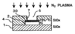
- etching process is carried out to form a via hole 6 .
- Nitrogen (N 2 ) plasma processing (a first nitrogen plasma processing) is simultaneously carried out during the etching process in the manufacturing method of this embodiment ( FIG. 1 , step 13 ). More specifically, as shown in FIG. 14E , the inter-layer film 4 is dry-etched through the mask of the photo resist 5 to expose the TiN film of the barrier metal layer 30 , forming the via hole 6 , and thereafter, the nitrogen plasma processing is carried out within the same apparatus. This eliminates the electric charge from the TiN film.
- a plasma stripping processing is carried out to strip the photo resist 5 ( FIG. 1 , step 106 ).
- a nitrogen plasma processing is carried out again (a second nitrogen plasma processing) ( FIG. 1 , step 104 ). This reduces the positive electric charge accumulated in the TiN film.
- an organic solvent-stripping processing is carried out to remove the residues 7 adhered onto the side walls of the via hole 6 ( FIG. 1 , step 15 ).
- An organic solvent-stripping processing includes three steps of: (1) wet processing by a liquid chemical solution; (2) rinsing by a rinse liquid; and (3) drying.
- the available rinse liquid of the above (2) step of rinsing may be prepared so that a resistivity thereof may be controlled to be equal to or lower than 0.3 [M ⁇ cm].
- Such rinse liquid available for this embodiment may be carbonated water containing carbon dioxide (CO 2 ) dissolved in pure water. In this case, the resistivity of the rinse liquid can be controlled by adjusting the quantity of carbon dioxide dissolved in pure water.
- the TiN layer of barrier metal layer 30 exposed to the bottom of the via hole 6 is partially eliminated via a radio frequency (RF) sputtering process by a thickness within a range from about 13 nm to 30 nm and more preferably by a thickness within a range from about 18 nm to 25 nm ( FIG. 1 , step 16 ).
- RF radio frequency
- TiN layer is partially eliminated by about 20 nm thick.
- the film thickness of TiN of regions other than the bottom of the via hole 6 is about 50 nm. This helps removing TiOn (titanium oxide), which has been generated on the surface of the TiN layer disposed on the bottom of the via hole 6 .
- a barrier metal (TiN) is formed in the via hole 6 by spatter processing, and after that, tungsten (W) is grown by a chemical vapor deposition (CVD). Thereafter, a chemical mechanical polishing (CMP) is carried out until SiOx of the inter-layer film 4 is exposed. Eventually, the via is formed.
- FIG. 16 is a cross sectional view showing the constitution of the via bottom in detail.
- the TiN film of the barrier metal layer 30 has a region, in which the via (a TiN film 32 and a W plug 34 ) is formed, and a top surface of the region is lower than that of other regions of the TiN film by a height or thickness d.
- the film thickness of the TiN film in the other region may be, for example, 50 nm.
- the height or the thickness d may be within a range of 13 nm to 30 nm, and more preferably within a range of 18 nm to 25 nm.
- FIG. 17 is a cross sectional view showing a constitution of a semiconductor device according to this embodiment.
- the semiconductor device has a constitution, in which a via is formed in a via hole 6 by the similar procedure as employed in the first embodiment described in reference to FIGS. 13A to 13C , FIGS. 14D to 14G , FIGS. 15H and 15I and FIG. 16 , and which further comprises a second aluminum interconnect line 38 formed thereon.
- a Ti film and a TiN film which will be a barrier metal layer 36 , are deposited on the via and the inter-layer film 4 by a sputtering process.
- an aluminum film for forming an aluminum interconnect line 38 is deposited on the barrier metal layer 36 .
- a Ti film and a TiN film for forming the barrier metal layer 40 are deposited on the aluminum film by a sputtering process.
- the sputtering process for depositing the aluminum film for forming the aluminum interconnect line 38 may be conducted at a temperature around 300 to 350 degree C., similarly as in the formation of the aluminum film 2 .
- the Ti film of the barrier metal layer 40 is grown by utilizing the remaining heat generated by the process for depositing the aluminum film.
- the production yield rate was improved up to nearly 100% according to the method for manufacturing the semiconductor device in this embodiment from about 20% for a conventional manufacturing method, by carrying out the various processing steps that has been described above.
- the production yield is meant to be a rate of via holes that are inspected and classified as non-defective, and the non-defective via holes were classified in the inspection when a resistance per one via hole was within a specific range.
- the conventional sputtering process for the Ti film in the conventional manufacturing method is generally carried out by utilizing remaining heat that has been generated in the sputtering process for the aluminum interconnect line, it is estimated that the wafer temperature for conducting the sputtering process for the Ti film should be around 170 to 180 degree C. Therefore, a comparative example of conducting a sputtering process for the Ti film at a temperature of about 170 to 180 degree C. was additionally carried out and the production yield of the comparative example (20%) was additionally employed.
- the production yields were improved by up to about 50% when the temperatures of the sputtering process for forming the Ti film for the barrier metal layer were set to a temperature within a range of from 200 degree C. to 225 degree C. It is also found in the figure that the production yields were deteriorated when the temperatures for depositing the Ti films were set to a temperature of 300 degree C. or 400 degree C., because the resistance thereof increases due to roughening of the surface of the TiN film.
- oxidation of the TiN film was inhibited by conducting the first nitrogen plasma processing or the second nitrogen plasma processing during the formation of the via hole to reduce positive electric charge accumulated in the TiN film, thereby significantly improving the production yield.
- the production yield was improved by conducting the UV irradiation as compared with the case of having no UV irradiation.
- FIG. 4 includes photographs showing the status of changing the surface charge distribution of three wafer samples No. 1 to No. 3 by conducting a nitrogen plasma processing to these wafers.
- the upper row of FIG. 4 includes photographs showing the electric charge distributions of the surfaces of wafers after depositing inter-layer films, and the lower row of FIG. 4 includes photographs showing the electric charge distributions of the surfaces of wafers after conducting the nitrogen plasma processing.
- FIG. 5 is a graph showing the relationship between the resistivity of a rinse liquid during the rinse processing using the rinse liquid in the organic solvent-stripping processing and the production yields of the obtained products, shown as step 15 of FIG. 1 .
- the resistivities of the rinse liquids were adjusted to obtain 0.15, 0.2, 0.3, 0.35, 0.4 or 0.5 [M ⁇ cm], respectively, and the cleaning processes with the respective rinse liquids were conducted.
- the resistivities of the rinse liquids were adjusted by selecting the quantity of carbon dioxide dissolved in pure water.
- the production yield was improved by controlling the resistivity of the rinse liquid to equal to or lower than 0.3 [M ⁇ cm].
- the lower limit of the resistivity of the rinse liquid is not particularly limited, the resistivity may be adjusted to, for example, 0.01 [M ⁇ cm].
- FIG. 6 is a graph showing relationships between the RF-spattered thickness during the RF sputtering processes for the TiN film disposed on the bottom of the via hole in the step 16 of FIG. 1 and the production yields of the resultant products.
- the production yields were obtained for the cases of: the RF-spattered thickness was 10 nm (the RF-spattered thickness was 20% of the non-sputtered film thickness); 12 nm (24%); 14 nm (28%); 16 nm (32%); 18 nm (36%); 20 nm (40%); 22 nm (44%); and 30 nm (60%).
- the production yields improved by increasing the RF-spattered thickness improved by having the RF-spattered thicknesses of equal to or larger than 13 nm, and more preferably equal to or larger than 18 nm.
- the RF-spattered thickness may be, for example, equal to or lower than 30 nm, and more preferably equal to or lower than 25 nm. This helps effectively removing titanium oxide from the semiconductor device having various types of interconnect patterns formed therein, without, for example, adversely affecting other layers such as the underlying aluminum interconnect lines.
- FIG. 7 is a graph showing the advantageous effects obtained by sequentially adding respective countermeasures stated above.
- FIG. 7 includes the results obtained by the processes of:
- a semiconductor device was manufactured in a similar method as described in the second embodiment. Heating process was included in the deposition of the Ti film for the barrier metal layer 30 , and the Ti film was formed at a temperature of about 200 degree C. Another Ti film for another barrier metal layer 40 was deposited by utilizing remaining heat that had been generated in the process for depositing an aluminum film ( 38 ). The results analyzed by employing an X-ray photoelectron spectroscopy (XPS) for (111) orientation of the TiN film of the barrier metal layer 30 and (111) orientation of the TiN film of the barrier metal layer 40 are shown in FIG. 18 . As can be seen from the peak intensities appeared in the chart, it is indicated that (111) orientation of the TiN film of the barrier metal layer 30 is higher by 20% than (111) orientation of the TiN film of the barrier metal layer 40 .
- XPS X-ray photoelectron spectroscopy
- the present invention has been described in relation to the configuration of employing SiOx for the inter-layer film 4 in the above embodiments, a person having ordinary skills in the art would appreciate that the present invention is not limited thereto, and the inter-layer film 4 may be formed by employing other materials such as SiOF.
Landscapes
- Internal Circuitry In Semiconductor Integrated Circuit Devices (AREA)
- Electrodes Of Semiconductors (AREA)
Abstract
Description
- (1): forming the via holes by the conventional manufacturing method (without any countermeasures described above);
- (2): depositing the TiN film via the sputtering process at a temperature of 200 degree C.;
- (3): irradiating thereto with UV, in addition to the above (2);
- (4): conducting the first nitrogen plasma processing thereto during the etching process for the via holes, in addition to the above (3);
- (5): conducting the second nitrogen plasma processing thereto after the plasma stripping, in addition to the above (4);
- (6): controlling the resistivity of the rinse liquid used in the organic stripping processing to equal to or lower than 0.3 [MΩ cm], in addition to (5); and
- (7): sputtering thereof to achieve the RF-spattered thickness of 20 nm, in addition to (6).
It should be noted that all the countermeasures described above were included in the process of the above (7).
Claims (21)
Applications Claiming Priority (4)
| Application Number | Priority Date | Filing Date | Title |
|---|---|---|---|
| JP2003174948 | 2003-06-19 | ||
| JP2003-174948 | 2003-06-19 | ||
| JP2004146464A JP4383248B2 (en) | 2003-06-19 | 2004-05-17 | Manufacturing method of semiconductor device |
| JP2004-146464 | 2004-05-17 |
Publications (2)
| Publication Number | Publication Date |
|---|---|
| US20040259374A1 US20040259374A1 (en) | 2004-12-23 |
| US7071116B2 true US7071116B2 (en) | 2006-07-04 |
Family
ID=33518585
Family Applications (1)
| Application Number | Title | Priority Date | Filing Date |
|---|---|---|---|
| US10/867,789 Expired - Lifetime US7071116B2 (en) | 2003-06-19 | 2004-06-16 | Semiconductor device and method for manufacturing same |
Country Status (2)
| Country | Link |
|---|---|
| US (1) | US7071116B2 (en) |
| JP (1) | JP4383248B2 (en) |
Cited By (2)
| Publication number | Priority date | Publication date | Assignee | Title |
|---|---|---|---|---|
| US20080166872A1 (en) * | 2005-08-10 | 2008-07-10 | Fujitsu Limited | Method of producing semiconductor device |
| US20090310723A1 (en) * | 2006-06-27 | 2009-12-17 | Kazuhisa Ishiguro | Automatic gain control circuit |
Families Citing this family (8)
| Publication number | Priority date | Publication date | Assignee | Title |
|---|---|---|---|---|
| JP4547289B2 (en) | 2005-03-25 | 2010-09-22 | ルネサスエレクトロニクス株式会社 | Manufacturing method of semiconductor device |
| JP2009033209A (en) * | 2008-11-10 | 2009-02-12 | Seiko Epson Corp | Semiconductor device and manufacturing method thereof |
| KR101674538B1 (en) * | 2011-03-24 | 2016-11-09 | 해성디에스 주식회사 | Method of forming metal pattern |
| US10354913B2 (en) | 2017-05-31 | 2019-07-16 | Taiwan Semiconductor Manufacturing Company, Ltd. | Chemical clean of semiconductor device |
| US10438813B2 (en) * | 2017-11-13 | 2019-10-08 | Alpha And Omega Semiconductor (Cayman) Ltd. | Semiconductor device having one or more titanium interlayers and method of making the same |
| CN109125809A (en) * | 2018-08-21 | 2019-01-04 | 华南理工大学 | To inhibit bacterial growth and promote the titanium surface and preparation method thereof of protein adherence |
| US20230411142A1 (en) * | 2022-06-16 | 2023-12-21 | Tokyo Electron Limited | Metal oxide precleaning prior to metal filling |
| US20240371654A1 (en) * | 2023-05-03 | 2024-11-07 | Applied Materials, Inc. | Silicon nitride damage-free dry etch method for tungsten removal in middle of line bottom-up tungsten integration |
Citations (3)
| Publication number | Priority date | Publication date | Assignee | Title |
|---|---|---|---|---|
| US5470792A (en) * | 1993-03-03 | 1995-11-28 | Nec Corporation | Method of manufacturing semiconductor device |
| JPH1032248A (en) | 1996-07-12 | 1998-02-03 | Yamaha Corp | Formation of tungsten film |
| US20030181031A1 (en) * | 2002-03-25 | 2003-09-25 | Kabushiki Kaisha Toshiba | Method for manufacturing a semiconductor device |
-
2004
- 2004-05-17 JP JP2004146464A patent/JP4383248B2/en not_active Expired - Fee Related
- 2004-06-16 US US10/867,789 patent/US7071116B2/en not_active Expired - Lifetime
Patent Citations (3)
| Publication number | Priority date | Publication date | Assignee | Title |
|---|---|---|---|---|
| US5470792A (en) * | 1993-03-03 | 1995-11-28 | Nec Corporation | Method of manufacturing semiconductor device |
| JPH1032248A (en) | 1996-07-12 | 1998-02-03 | Yamaha Corp | Formation of tungsten film |
| US20030181031A1 (en) * | 2002-03-25 | 2003-09-25 | Kabushiki Kaisha Toshiba | Method for manufacturing a semiconductor device |
Non-Patent Citations (1)
| Title |
|---|
| S. Gwo, et al., "Local Electric-Field-Induced Oxidation of Titanium Nitride Films". Applied Physics Letters, vol. 74. No. 8, Feb. 22, 1999, pp. 1090-1092. |
Cited By (3)
| Publication number | Priority date | Publication date | Assignee | Title |
|---|---|---|---|---|
| US20080166872A1 (en) * | 2005-08-10 | 2008-07-10 | Fujitsu Limited | Method of producing semiconductor device |
| US7811936B2 (en) * | 2005-08-10 | 2010-10-12 | Fujitsu Semiconductor Limited | Method of producing semiconductor device |
| US20090310723A1 (en) * | 2006-06-27 | 2009-12-17 | Kazuhisa Ishiguro | Automatic gain control circuit |
Also Published As
| Publication number | Publication date |
|---|---|
| JP2005033182A (en) | 2005-02-03 |
| JP4383248B2 (en) | 2009-12-16 |
| US20040259374A1 (en) | 2004-12-23 |
Similar Documents
| Publication | Publication Date | Title |
|---|---|---|
| US7320942B2 (en) | Method for removal of metallic residue after plasma etching of a metal layer | |
| US7259091B2 (en) | Technique for forming a passivation layer prior to depositing a barrier layer in a copper metallization layer | |
| US20060102197A1 (en) | Post-etch treatment to remove residues | |
| US20090075479A1 (en) | Method of manufacturing semiconductor device | |
| Merchant et al. | Copper interconnects for semiconductor devices | |
| US7071116B2 (en) | Semiconductor device and method for manufacturing same | |
| CN101064253A (en) | Method for removing masking materials with reduced low-k dielectric material damage | |
| US20110034025A1 (en) | Method for Forming Contact Hole Structure | |
| US6174798B1 (en) | Process for forming metal interconnect stack for integrated circuit structure | |
| US7253124B2 (en) | Process for defect reduction in electrochemical plating | |
| US6554004B1 (en) | Method for removing etch residue resulting from a process for forming a via | |
| US20030181031A1 (en) | Method for manufacturing a semiconductor device | |
| Ueno et al. | Cleaning of CHF 3 plasma-etched SiO 2/SiN/Cu via structures using a hydrogen plasma, an oxygen plasma, and hexafluoroacetylacetone vapors | |
| KR101532456B1 (en) | Bevel plasma treatment to enhance wet edge clean | |
| US11688604B2 (en) | Method for using ultra thin ruthenium metal hard mask for etching profile control | |
| US20050048776A1 (en) | Integrated circuit copper plateable barriers | |
| US6174819B1 (en) | Low temperature photoresist removal for rework during metal mask formation | |
| US8399360B1 (en) | Process for post contact-etch clean | |
| US6534415B2 (en) | Method of removing polymer residues after tungsten etch back | |
| US7344998B2 (en) | Wafer recovering method, wafer, and fabrication method | |
| US20040018743A1 (en) | Method for removing photoresist after metal layer etching in a semiconductor device | |
| US8153518B2 (en) | Method for fabricating metal interconnection of semiconductor device | |
| JP2008085297A (en) | Manufacturing method of semiconductor device | |
| US20070037381A1 (en) | Method for fabricating Al metal line | |
| JPH1192956A (en) | Method for plating substrate |
Legal Events
| Date | Code | Title | Description |
|---|---|---|---|
| AS | Assignment |
Owner name: NEC ELECTRONICS CORPORATION, JAPAN Free format text: ASSIGNMENT OF ASSIGNORS INTEREST;ASSIGNOR:YASUDA, MAKOTO;REEL/FRAME:015482/0021 Effective date: 20040602 |
|
| FEPP | Fee payment procedure |
Free format text: PAYOR NUMBER ASSIGNED (ORIGINAL EVENT CODE: ASPN); ENTITY STATUS OF PATENT OWNER: LARGE ENTITY |
|
| STCF | Information on status: patent grant |
Free format text: PATENTED CASE |
|
| FPAY | Fee payment |
Year of fee payment: 4 |
|
| AS | Assignment |
Owner name: RENESAS ELECTRONICS CORPORATION, JAPAN Free format text: CHANGE OF NAME;ASSIGNOR:NEC ELECTRONICS CORPORATION;REEL/FRAME:025525/0127 Effective date: 20100401 |
|
| FPAY | Fee payment |
Year of fee payment: 8 |
|
| AS | Assignment |
Owner name: RENESAS ELECTRONICS CORPORATION, JAPAN Free format text: CHANGE OF ADDRESS;ASSIGNOR:RENESAS ELECTRONICS CORPORATION;REEL/FRAME:044928/0001 Effective date: 20150806 |
|
| MAFP | Maintenance fee payment |
Free format text: PAYMENT OF MAINTENANCE FEE, 12TH YEAR, LARGE ENTITY (ORIGINAL EVENT CODE: M1553) Year of fee payment: 12 |