US7009602B2 - Method of driving plasma display panel - Google Patents
Method of driving plasma display panel Download PDFInfo
- Publication number
- US7009602B2 US7009602B2 US09/891,664 US89166401A US7009602B2 US 7009602 B2 US7009602 B2 US 7009602B2 US 89166401 A US89166401 A US 89166401A US 7009602 B2 US7009602 B2 US 7009602B2
- Authority
- US
- United States
- Prior art keywords
- electrodes
- pulse
- display
- discharge
- sustain
- Prior art date
- Legal status (The legal status is an assumption and is not a legal conclusion. Google has not performed a legal analysis and makes no representation as to the accuracy of the status listed.)
- Expired - Fee Related, expires
Links
- 238000000034 method Methods 0.000 title claims abstract description 32
- 230000037452 priming Effects 0.000 claims description 61
- 230000008030 elimination Effects 0.000 claims description 22
- 238000003379 elimination reaction Methods 0.000 claims description 22
- 230000008859 change Effects 0.000 claims description 15
- OAICVXFJPJFONN-UHFFFAOYSA-N Phosphorus Chemical compound [P] OAICVXFJPJFONN-UHFFFAOYSA-N 0.000 description 16
- 238000000926 separation method Methods 0.000 description 9
- 239000010410 layer Substances 0.000 description 7
- 239000007789 gas Substances 0.000 description 5
- 239000000126 substance Substances 0.000 description 5
- 230000007423 decrease Effects 0.000 description 4
- 238000009825 accumulation Methods 0.000 description 3
- 230000006870 function Effects 0.000 description 3
- 239000012212 insulator Substances 0.000 description 3
- 150000001450 anions Chemical class 0.000 description 2
- 239000003086 colorant Substances 0.000 description 2
- 230000003247 decreasing effect Effects 0.000 description 2
- 239000011159 matrix material Substances 0.000 description 2
- 230000004044 response Effects 0.000 description 2
- 230000003213 activating effect Effects 0.000 description 1
- 230000015572 biosynthetic process Effects 0.000 description 1
- 230000015556 catabolic process Effects 0.000 description 1
- 238000010276 construction Methods 0.000 description 1
- 238000007796 conventional method Methods 0.000 description 1
- 238000006731 degradation reaction Methods 0.000 description 1
- 239000011521 glass Substances 0.000 description 1
- 229910052734 helium Inorganic materials 0.000 description 1
- 239000001307 helium Substances 0.000 description 1
- SWQJXJOGLNCZEY-UHFFFAOYSA-N helium atom Chemical compound [He] SWQJXJOGLNCZEY-UHFFFAOYSA-N 0.000 description 1
- 230000006386 memory function Effects 0.000 description 1
- 238000012986 modification Methods 0.000 description 1
- 230000004048 modification Effects 0.000 description 1
- 229910052754 neon Inorganic materials 0.000 description 1
- GKAOGPIIYCISHV-UHFFFAOYSA-N neon atom Chemical compound [Ne] GKAOGPIIYCISHV-UHFFFAOYSA-N 0.000 description 1
- 239000002245 particle Substances 0.000 description 1
- 239000011241 protective layer Substances 0.000 description 1
- 230000000630 rising effect Effects 0.000 description 1
- 238000004544 sputter deposition Methods 0.000 description 1
- 229910052724 xenon Inorganic materials 0.000 description 1
- FHNFHKCVQCLJFQ-UHFFFAOYSA-N xenon atom Chemical compound [Xe] FHNFHKCVQCLJFQ-UHFFFAOYSA-N 0.000 description 1
Images


Classifications
-
- G—PHYSICS
- G09—EDUCATION; CRYPTOGRAPHY; DISPLAY; ADVERTISING; SEALS
- G09G—ARRANGEMENTS OR CIRCUITS FOR CONTROL OF INDICATING DEVICES USING STATIC MEANS TO PRESENT VARIABLE INFORMATION
- G09G3/00—Control arrangements or circuits, of interest only in connection with visual indicators other than cathode-ray tubes
- G09G3/20—Control arrangements or circuits, of interest only in connection with visual indicators other than cathode-ray tubes for presentation of an assembly of a number of characters, e.g. a page, by composing the assembly by combination of individual elements arranged in a matrix no fixed position being assigned to or needed to be assigned to the individual characters or partial characters
- G09G3/22—Control arrangements or circuits, of interest only in connection with visual indicators other than cathode-ray tubes for presentation of an assembly of a number of characters, e.g. a page, by composing the assembly by combination of individual elements arranged in a matrix no fixed position being assigned to or needed to be assigned to the individual characters or partial characters using controlled light sources
- G09G3/28—Control arrangements or circuits, of interest only in connection with visual indicators other than cathode-ray tubes for presentation of an assembly of a number of characters, e.g. a page, by composing the assembly by combination of individual elements arranged in a matrix no fixed position being assigned to or needed to be assigned to the individual characters or partial characters using controlled light sources using luminous gas-discharge panels, e.g. plasma panels
- G09G3/288—Control arrangements or circuits, of interest only in connection with visual indicators other than cathode-ray tubes for presentation of an assembly of a number of characters, e.g. a page, by composing the assembly by combination of individual elements arranged in a matrix no fixed position being assigned to or needed to be assigned to the individual characters or partial characters using controlled light sources using luminous gas-discharge panels, e.g. plasma panels using AC panels
- G09G3/291—Control arrangements or circuits, of interest only in connection with visual indicators other than cathode-ray tubes for presentation of an assembly of a number of characters, e.g. a page, by composing the assembly by combination of individual elements arranged in a matrix no fixed position being assigned to or needed to be assigned to the individual characters or partial characters using controlled light sources using luminous gas-discharge panels, e.g. plasma panels using AC panels controlling the gas discharge to control a cell condition, e.g. by means of specific pulse shapes
- G09G3/292—Control arrangements or circuits, of interest only in connection with visual indicators other than cathode-ray tubes for presentation of an assembly of a number of characters, e.g. a page, by composing the assembly by combination of individual elements arranged in a matrix no fixed position being assigned to or needed to be assigned to the individual characters or partial characters using controlled light sources using luminous gas-discharge panels, e.g. plasma panels using AC panels controlling the gas discharge to control a cell condition, e.g. by means of specific pulse shapes for reset discharge, priming discharge or erase discharge occurring in a phase other than addressing
- G09G3/2927—Details of initialising
-
- G—PHYSICS
- G09—EDUCATION; CRYPTOGRAPHY; DISPLAY; ADVERTISING; SEALS
- G09G—ARRANGEMENTS OR CIRCUITS FOR CONTROL OF INDICATING DEVICES USING STATIC MEANS TO PRESENT VARIABLE INFORMATION
- G09G3/00—Control arrangements or circuits, of interest only in connection with visual indicators other than cathode-ray tubes
- G09G3/20—Control arrangements or circuits, of interest only in connection with visual indicators other than cathode-ray tubes for presentation of an assembly of a number of characters, e.g. a page, by composing the assembly by combination of individual elements arranged in a matrix no fixed position being assigned to or needed to be assigned to the individual characters or partial characters
- G09G3/22—Control arrangements or circuits, of interest only in connection with visual indicators other than cathode-ray tubes for presentation of an assembly of a number of characters, e.g. a page, by composing the assembly by combination of individual elements arranged in a matrix no fixed position being assigned to or needed to be assigned to the individual characters or partial characters using controlled light sources
- G09G3/28—Control arrangements or circuits, of interest only in connection with visual indicators other than cathode-ray tubes for presentation of an assembly of a number of characters, e.g. a page, by composing the assembly by combination of individual elements arranged in a matrix no fixed position being assigned to or needed to be assigned to the individual characters or partial characters using controlled light sources using luminous gas-discharge panels, e.g. plasma panels
- G09G3/288—Control arrangements or circuits, of interest only in connection with visual indicators other than cathode-ray tubes for presentation of an assembly of a number of characters, e.g. a page, by composing the assembly by combination of individual elements arranged in a matrix no fixed position being assigned to or needed to be assigned to the individual characters or partial characters using controlled light sources using luminous gas-discharge panels, e.g. plasma panels using AC panels
- G09G3/291—Control arrangements or circuits, of interest only in connection with visual indicators other than cathode-ray tubes for presentation of an assembly of a number of characters, e.g. a page, by composing the assembly by combination of individual elements arranged in a matrix no fixed position being assigned to or needed to be assigned to the individual characters or partial characters using controlled light sources using luminous gas-discharge panels, e.g. plasma panels using AC panels controlling the gas discharge to control a cell condition, e.g. by means of specific pulse shapes
- G09G3/293—Control arrangements or circuits, of interest only in connection with visual indicators other than cathode-ray tubes for presentation of an assembly of a number of characters, e.g. a page, by composing the assembly by combination of individual elements arranged in a matrix no fixed position being assigned to or needed to be assigned to the individual characters or partial characters using controlled light sources using luminous gas-discharge panels, e.g. plasma panels using AC panels controlling the gas discharge to control a cell condition, e.g. by means of specific pulse shapes for address discharge
- G09G3/2932—Addressed by writing selected cells that are in an OFF state
-
- G—PHYSICS
- G09—EDUCATION; CRYPTOGRAPHY; DISPLAY; ADVERTISING; SEALS
- G09G—ARRANGEMENTS OR CIRCUITS FOR CONTROL OF INDICATING DEVICES USING STATIC MEANS TO PRESENT VARIABLE INFORMATION
- G09G2310/00—Command of the display device
- G09G2310/02—Addressing, scanning or driving the display screen or processing steps related thereto
- G09G2310/0224—Details of interlacing
-
- G—PHYSICS
- G09—EDUCATION; CRYPTOGRAPHY; DISPLAY; ADVERTISING; SEALS
- G09G—ARRANGEMENTS OR CIRCUITS FOR CONTROL OF INDICATING DEVICES USING STATIC MEANS TO PRESENT VARIABLE INFORMATION
- G09G2310/00—Command of the display device
- G09G2310/06—Details of flat display driving waveforms
- G09G2310/066—Waveforms comprising a gently increasing or decreasing portion, e.g. ramp
-
- G—PHYSICS
- G09—EDUCATION; CRYPTOGRAPHY; DISPLAY; ADVERTISING; SEALS
- G09G—ARRANGEMENTS OR CIRCUITS FOR CONTROL OF INDICATING DEVICES USING STATIC MEANS TO PRESENT VARIABLE INFORMATION
- G09G2320/00—Control of display operating conditions
- G09G2320/02—Improving the quality of display appearance
- G09G2320/0228—Increasing the driving margin in plasma displays
-
- G—PHYSICS
- G09—EDUCATION; CRYPTOGRAPHY; DISPLAY; ADVERTISING; SEALS
- G09G—ARRANGEMENTS OR CIRCUITS FOR CONTROL OF INDICATING DEVICES USING STATIC MEANS TO PRESENT VARIABLE INFORMATION
- G09G2320/00—Control of display operating conditions
- G09G2320/02—Improving the quality of display appearance
- G09G2320/0238—Improving the black level
Definitions
- This invention relates to plasma display panels, and especially to a method of driving plasma display panels.
- a plasma display panel (abbreviated to “PDP” below) has a flat structure and a high display contrast without flickering. Moreover, it has many characteristics: for example, it can be made into a relatively big screen, it has a fast response, and, being of the self-fluorescent type, it can be made to fluoresce in multi-color by the use of phosphors. For this reason, its application has been expanding in the fields of large size public display device and color television, etc., in recent years.
- PDP has the alternating current discharge type (AC type), in which, the electrodes are covered by a dielectric substance, and is operated by a condition of alternating current discharge indirectly, and the direct current discharge type (DC type), in which, the electrodes are exposed to the discharge space, and is operated by a condition of direct current discharges.
- AC type alternating current discharge type
- DC type direct current discharge type
- the alternating current discharge type there is the memory drive type that uses the memory of the discharge cells as its drive method, and the refresh drive type that does not use that method.
- the brightness of PDP is approximately proportional to the number of discharges, that is, the repetition number of the pulse voltage, regardless of the memory drive type or the refresh drive type.
- the refresh drive type as the display capacity becomes larger, brightness decreases and it is mainly used for PDP with small display capacity.
- FIG. 1 is a perspective exploded view showing an example of the structure of the display cells in an alternating current discharge memory drive type PDP that is disclosed in Japanese Patent No. 2629944 (Japanese Unexamined Patent Publications No. 2-220330) and Japanese Unexamined Patent Publication No. 2000-39866.
- This PDP seals the discharge gas in between two insulator plates 1 and 2 of the front surface and the rear surface made of glass plates.
- the transparent sustain electrodes 3 and the bus electrodes 4 which are placed coincident with the sustain electrodes 3 to reduce electrode resistance, are formed.
- phosphor 8 is coated on the dielectric substance layer 11 between the separation walls 7 , and the side surfaces of the separation walls. To display the various colors, the phosphor 8 is painted and arranged into the three primary colors of red, green, and blue. In between the insulator plates 1 and 2 , a discharge gas space 6 filled with a discharge gas of helium, neon, xenon and the like, or combinations thereof, is formed.
- the ultraviolet light generated by the discharge of the foregoing discharge gas is converted into the visible light 12 by the phosphor 8 .
- Every sustain electrode 3 becomes an electrode shared by the upper and lower display cell.
- FIG. 2 shows a vertical cross-sectional view of the display cells in the alternating current discharge memory drive type PDP shown in FIG. 1 .
- the discharge operation of the selected display cells will be explained with reference to FIG. 2 .
- the equivalent internal voltage due to the accumulation of electrical charges decreases the effective voltage inside the cell as well as the growth of the discharge, because of its opposite polarity to the foregoing pulse voltage. Even if the foregoing pulse voltage maintains a constant value, the discharge cannot be maintained, and will eventually stop.
- a sustain discharge pulse that is a pulse voltage of the same polarity as the wall voltage is applied between a neighboring sustain electrode pair and as the contribution of the wall voltage, being an effective voltage, is superimposed and even the voltage amplitude of the sustain discharge pulse is low, thus, discharge start voltage can be superseded and discharge occurs.
- This function is the aforementioned memory function.
- FIG. 3 is an explanatory drawing showing the schematic structure of the PDP formed by arranging in a matrix the display cells shown in FIG. 2 .
- PDP 13 is a dot matrix panel for display use, in which display cells 14 are arranged into m ⁇ n rows and columns.
- the sustain electrodes E 1 , E 2 , . . . , Em are placed mutually in parallel as row electrodes.
- the data electrodes D 1 , D 2 , . . . , Dn are placed orthogonally with respect to the sustain electrodes as column electrodes.
- FIGS. 4 and 5A to 5 E show respectively the drive waveform chart and modal drawing showing the change of the charged condition in the priming discharge period for the foregoing PDP disclosed in Japanese Patent Unexamined Publication No. 9-244573.
- W Ea , W Eb , W Ec , W Ed are sustain electrode drive pulses applied to the sustain electrodes Ea, Eb, Ec, Ed.
- W d is a data electrode drive pulse applied to data electrodes D i (1 ⁇ i ⁇ n).
- Sustain electrodes Ea indicates the (1+4K)-th sustain electrodes E 1 , E 5 , E 9 . . .
- sustain electrodes Eb indicates the (2+4K)-th sustain electrodes E 2 , E 6 , E 10 . . .
- sustain electrodes Ec indicates the (3+4K)-th sustain electrodes E 3 , E 7 , E 11 . . .
- sustain electrodes Ed indicates the (4+4K)-th sustain electrodes E 4 , E 8 , E 12 .
- K is 0 or a positive integer.
- the symbol ⁇ in the figure represents discharge.
- a drive period consists of a priming discharge period, a write discharge period, and a sustain discharge period. By repeating these, desired image displays can be obtained.
- the priming discharge period is a period to reset the previous history, and to generate active particles and wall charges in the discharge gas space.
- the write discharge period is a period in which, according to the display data, the ON/OFF of the display cells are selectively discharged.
- the sustain discharge period is a period in which discharges in the display cells selected in the write discharge period are repeated, and brightness is controlled.
- the sustain electrodes are divided into four electrode groups.
- the first group consists of the combination of the (1+4K)-th sustain electrodes counting from one side (the side of the foremost line) of the electrode arrangement.
- the second group is the combination of the (2+4K)-th sustain electrodes.
- the third group is that of the (3+4K)-th sustain electrodes, and the fourth group is that of the (4+4K)-th sustain electrodes.
- K is 0 or a positive integer.
- FIG. 4 shows the drive waveforms of these four groups of sustain electrodes Ea, Eb, Ec, Ed and the data electrodes.
- priming discharge pulse Pp 1 of positive polarity is applied to sustain electrodes Eb, Ed to produce discharges in all the lines.
- FIG. 5A in between sustain electrodes Ea, Ec, and sustain electrodes Eb, Ed, the polarities of the wall charges are different, and between the two lines corresponding to each of the sustain electrodes, charge conditions of the same polarity are formed. That is, taking the separation walls as mirror surfaces, the charge condition at every sustain electrode has mirror symmetry. With the mirror symmetry intact, when a scan pulse Pw is applied to each electrode, two lines would have been selected.
- priming discharge pulse Pp 2 of negative polarity is applied to the sustain electrode Eb, and at the same time, priming discharge pulse Pp 3 of positive polarity is applied to the sustain electrode Ec.
- priming discharge pulse Pp 3 of positive polarity is applied to the sustain electrode Ea, and at the same time, priming discharge pulse Pp 2 of negative polarity is applied to the sustain electrode Ed.
- the peak values of the priming discharge pulses Pp 2 , Pp 3 are chosen to be values that would be sufficient to generate discharges only by applying both of the priming discharge pulses Pp 2 , Pp 3 , as illustrated in FIGS. 5 B and 5 C.
- priming discharge elimination pulse Ppe of positive polarity is applied to the sustain electrodes Ea, Ec, and at timing (e), priming discharge elimination pulse Ppe of positive polarity is applied to the sustain electrodes Eb, Ed to produce elimination discharges to remove unwanted wall charges.
- the sustain electrodes are sequentially selected one by one, and a scan pulse of negative polarity Pw is applied, in lines where wall charges of negative polarity exist, opposite discharges occur.
- selecting sequentially from the second sustain electrode in the electrode arrangement will be acceptable.
- FIGS. 5F to 5H are drawings showing the charge conditions due to write discharge and sustain discharge.
- FIG. 5F represents a summary of the write discharge of every display cell (timing (f)), and the charge condition is after the finish of the writing of all the display cells.
- timing (f) the charge condition is after the finish of the writing of all the display cells.
- sustain discharges are repeated simultaneously in all the written-in display cells.
- sustain discharge starts at every other line with a lag of one time, they all stop at the same time.
- the number of sustain discharges is different for every line, and brightness becomes different.
- Japanese Unexamined Patent Publication No. 10-3280 has suggested a plasma display panel in which first electrodes are grouped into K-th electrodes and (K+1)-th electrodes wherein K is an even number, and second electrodes are grouped into M-th electrode and (M+1)-th electrodes wherein M is an even number.
- the K-th and (K+1)-th electrodes and the M-th and (M+1)-th electrodes are simultaneously driven in both reset and address periods.
- a phase of a pulse in the K-th and M-th electrodes is retarded by 180 degrees relative to a phase of a pulse in the (K+1)-th and (M+1)-th electrodes.
- Japanese Unexamined Patent Publication No. 10-207417 has suggested a method of driving a plasma display panel, in which reset discharges are carried out at different timings in fields, and a discharge is not carried out in a reset period in a discharge cell which does not contribute to displaying.
- the present invention provides a method of driving a plasma display panel comprising a plurality of mutually parallel first electrodes, and a plurality of second electrodes separated from and perpendicular to the first electrodes, the intersection points of neighboring pairs of the first electrode pairs and the second electrode pairs forming an unit display cell, the method comprising the step of reversing the potentials between the electrodes at the time of write discharge carried out between the odd-numbered the first electrodes and even-numbered the first electrodes, and the second electrodes, to each other.
- a scan pulse of negative polarity from the first base potential is applied sequentially, and then corresponding to the scan pulse of negative polarity, at the second electrodes, a data pulse of positive polarity from the second base potential is applied, and at the even-numbered (odd-numbered) first electrodes, a scan pulse of positive polarity from the third base potential is applied sequentially, and then corresponding to the scan pulse of positive polarity, at the second electrodes, a data pulse of negative polarity from the fourth base potential is applied to carry out the write discharges.
- At least one of the amplitude of the scan pulse of negative polarity and the amplitude of the scan pulse of positive polarity, and, the amplitude of the data pulse of positive polarity and the amplitude of the data pulse of negative polarity, are different.
- the third base potential of the scan pulse of positive polarity is set at a higher potential than the first base potential of the scan pulse of negative polarity, and the second base potential of the data pulse of positive polarity and the reach potential of the data pulse of negative polarity are made to be the same potential, and the fourth base potential of the data pulse of negative polarity and the reach potential of the data pulse of positive polarity are made to be the same potential.
- the first base potential of the scan pulse of negative polarity and the third base potential of the scan pulse of positive polarity are made to be at the same potential, and, the second base potential of the data pulse of positive polarity and the fourth base potential of the data pulse of negative polarity are made to be at the same potential.
- a write cancel pulse is applied at the time of write discharge.
- sustain discharges are carried out between the first electrodes neighboring all the display cells.
- a discharge period in which the electrical charge conditions in all the display cells are reset, is set.
- the discharge period in which electrical charge conditions are reset, is a sustain elimination discharge that resets only the display cells that has sustain discharged in the previous sustain discharge period, or a priming discharge that causes discharges in all display cells, or a combination of sustain elimination discharge and priming discharge.
- priming discharges are made to occur simultaneously in all display cells, and the rise, or, time of rise, of the pulse that causes the occurrence of priming discharges is below 10 V/ ⁇ s.
- the second electrodes are set in an island form in every display cell, and the island-formed parts are positioned opposite the first electrodes that carry out the write discharges.
- the sustain electrodes are divided according to their odd or even order.
- the wall charges on the sustain electrodes that are formed by write discharge are unified to be positive or negative, the start of sustain discharge can be made simultaneous in all the selected display cells.
- the brightness of every display line can be unified, and stabilized drive performance can be obtained.
- the setting of a discharge period that resets the charge conditions of all the display cells before the write discharge improves write discharge performance. Also, as the fluorescent brightness of priming discharge can be suppressed to be low, contrast is enhanced, and good picture quality can be obtained.
- FIG. 1 is a perspective exploded view of conventional PDP.
- FIG. 2 shows a vertical cross-sectional view of the PDP shown in FIG. 1 .
- FIG. 3 shows the electrode construction of conventional PDP.
- FIG. 4 is a drive waveform chart showing the conventional PDP drive method.
- FIGS. 5A to 5E are modal drawings of the charge condition change of the priming discharge period in conventional PDP drive method
- FIGS. 5F to 5H are modal drawings of the charge condition change of the write discharge period and sustain discharge period in the conventional PDP drive method.
- FIG. 6 is a drive waveform chart showing the PDP drive method in accordance with the first embodiment of this invention.
- FIGS. 7A to 7H are modal drawings showing the charge condition change in the PDP drive method in accordance with the first embodiment of this invention.
- FIG. 8 is a perspective exploded view of the PDP in accordance with the first embodiment of this invention.
- FIG. 9 is a perspective projection of the top plan view showing with an emphasis on the electrodes and separation walls of the PDP in accordance with the first embodiment of this invention.
- FIG. 10 shows a vertical cross-sectional view of the PDP shown in FIG. 8 .
- FIG. 11 shows a vertical cross-sectional view of the PDP in accordance with the second embodiment of this invention.
- FIG. 12 shows a vertical cross-sectional view of the PDP in accordance with the third embodiment of this invention.
- FIG. 13 is a drive waveform chart showing the PDP drive method in accordance with the second embodiment of this invention.
- FIG. 14 is a drive waveform chart showing the PDP drive method in accordance with the third embodiment of this invention.
- FIGS. 15A to 15H are modal drawings showing the charge condition change in the PDP drive method in accordance with the third embodiment of this invention.
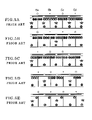
- FIG. 6 shows the drive waveform of the first example of embodiment.
- the sustain electrodes consist of 8 stripes.
- W E1 , W E2 , . . . , W E8 , the drive waveform of the sustain electrodes E 1 , E 2 , . . . , E 8 , and the W d , the drive waveform of the data electrode, are shown.
- a priming discharge pulse of slowly rising voltage is applied to the odd-numbered sustain electrodes to produce priming discharges in all display cells.
- a priming discharge elimination pulse of slowly falling voltage is applied.
- the potential of the even-numbered sustain electrodes has been raised up to about the potential of the sustain voltage, the potentials of the odd-numbered and even-numbered sustain electrodes reverse, and discharges occur.
- the potential change of the priming discharge pulse and the priming discharge elimination pulse is slow, if the potential of the display cells is slightly over the discharge start voltage, weak discharges occur.
- the wall charges so produced are arranged on the electrodes so that, by addition with the externally applied voltage, the potential is slightly lower than the discharge start voltage.
- the occurrence or non-occurrence of discharges can be selected to eliminate the wall charges.
- the meaning of elimination includes not only the elimination of the wall charges, but also the adjustment of the wall charges, in order to smoothly carrying out the write discharge and the sustain discharge.
- the meaning of elimination includes not only the elimination of the wall charges, but also the adjustment of the wall charges, in order to smoothly carrying out the write discharge and the sustain discharge.
- scan pulses are sequentially applied to the odd-numbered sustain electrodes. Furthermore, corresponding to the scan pulses, by applying data pulses to the data electrodes, discharges are produced between the sustain electrodes and the data electrodes.
- the scan pulses are applied in the negative direction from the base potential that is the standard, that is, pulses of negative polarity.
- data pulses are applied in the positive direction from the GND potential that is the standard, that is, pulses of positive polarity.
- the potential of the even-numbered sustain electrodes is higher than the potential (here, GND potential) of the odd-numbered sustain electrodes under the condition that scan pulses are applied. It induces discharges between the odd-numbered sustain electrodes and the data electrodes, and is made to be a potential that is about that which can produce discharges between the odd-numbered sustain electrodes and the even-numbered sustain electrodes. Specifically, the potential of these even-numbered sustain electrodes is about the voltage of the sustain voltage.
- scan pulses are sequentially applied to the even-numbered sustain electrode. Furthermore, corresponding to the scan pulses, by applying data pulses to the data electrodes, discharges are produced between the sustain electrodes and the data electrodes.
- the scan pulses are applied in the positive direction from a base potential that is about the sustain voltage that is the standard, that is, pulses of positive polarity.
- data pulses are applied in the negative direction from the data voltage that is the standard, that is, pulses of negative polarity.
- the potential of the odd-numbered sustain electrodes is lower than the potential of the even-numbered sustain electrodes under the condition that scan pulses are applied. It induces discharges between the odd-numbered sustain electrodes and the data electrodes, and is made to be a potential that is about that which can produce discharges between the odd-numbered sustain electrodes and the even-numbered sustain electrodes.
- the potential of these even-numbered sustain electrodes is about the voltage of the data voltage, by setting it equal to the standard potential of the data pulse or higher, discharge between odd-numbered sustain electrodes and the data electrodes can be suppressed.
- this write discharge positive wall charges are accumulated on the odd-numbered sustain electrodes and the data electrodes, and negative wall charges are accumulated on the even-numbered sustain electrodes.
- FIG. 6 shows the change of the wall discharges in the case of selective fluorescence in the display cell formed by the sustain electrode E 1 and the sustain electrode E 2 , and the display cell formed by the sustain electrode E 2 and the sustain electrode E 3 , in the write discharge period and the sustain discharge period. Moreover, in the priming discharge period, as discharges occur similarly in all the display cells, the change of wall charges is omitted.
- the sustain elimination pulse applies to the odd-numbered sustain electrodes a pulse that slowly drops from the potential of the sustain voltage to the GND potential, to produce weak discharges in display cells in which sustain discharges have occurred, to eliminate the wall charges.
- the elimination mentioned here is not limited to eliminating all the wall charges, but includes also adjusting the amount of wall charges that should make the carrying out of the subsequent priming discharge, the write discharge and the sustain discharge smooth.
- FIGS. 7A to 7H show the change of the charge condition inside the display cells from priming discharge to sustain removal discharge.
- FIGS. 7A to 7H correspond to the timings (A) to (H) in FIG. 6 .
- timing (A) when a priming pulse of voltage Vp is applied to the odd-numbered sustain electrodes, and at the same time, the even-numbered sustain electrodes are reduced to a 0 V potential discharges occur between the sustain electrodes of all the display cells.
- the wall charges are accumulated with a polarity of negative on the odd-numbered sustain electrodes, and positive on the even-numbered sustain electrodes.
- the priming discharge pulse is a pulse that rises slowly, the discharge is weak, and the amount of wall charges formed is also small.
- a priming discharge elimination pulse that raises the potential of the even-numbered sustain electrodes to a voltage of Vs, and reduces the odd-numbered sustain electrodes slowly to a 0 V potential is applied.
- the discharge at this time is weak and works to reduce the amount of wall charges formed at timing (A).
- Timing (C) is the write timing of the first line.
- the sustain electrode E 1 is applied with a scan pulse of negative polarity with reference to voltage Vbw as the standard potential, and reduced to a potential of 0V.
- Vbw voltage
- Vd voltage
- the wall charges formed in the priming discharge period is superimposed, and supersedes the discharge start voltage, and opposite discharges occur between the sustain electrode E 1 and the data electrode.
- Timing (D) is the write timing of the second line.
- the sustain electrode E 2 is applied with a scan pulse of positive polarity with reference to voltage Vs as the standard potential, and raised to a potential of Vw.
- the data electrode is applied with a data pulse of negative polarity with reference to voltage Vd as the standard potential, and reduced to a potential of 0V, even with consideration of the canceled contribution due to the wall charges formed in the priming discharge period, the discharge start potential is superseded, and opposite discharge occurs between the sustain electrode E 2 and the data electrode.
- Timing (E) is the timing of the first sustain discharge. If the odd-numbered sustain electrode is put at a voltage of Vs, and the even-numbered sustain electrodes at a voltage of 0 V, in the first line and the second line in which write discharges have occurred, the voltage of the wall charges after the priming discharge is superimposed onto the voltage Vs and supersedes the discharge start voltage, and opposite discharge occurs simultaneously in the two display cells.
- the data electrode is at 0V, as this is at the same potential as the even-numbered sustain electrode of low potential, accompanying the occurrence of sustain discharges, it changes to the condition of accumulation of positive wall charges.
- Timing (F) is the second timing of sustain discharge
- timing (G) is the last timing of sustain discharge. As they have respectively potentials opposite to the potential of the sustain electrodes at the time of the previous sustain discharge, sustain discharges of the written-in first line and second line occur.
- Timing (H) is the timing of sustain discharge elimination.
- the voltage of the even-numbered sustain electrodes is raised to Vs, and then to the odd-numbered sustain electrodes, the priming discharge elimination pulse is applied and slowly reduced down to the potential of 0 V.
- the discharge is as weak as at the time of priming discharge elimination, and the amount of wall charges decreases, from now on, wall charges are adjusted so that even if a sustain pulse is applied, sustain discharge would not happen.
- the amplitude of the data pulse of positive polarity is about the same as that of the data pulse of negative polarity, the application of a data electrode drive circuit that is optimized with respect to voltage tolerance is easy.
- FIG. 8 shows a perspective exploded view of the PDP.
- FIG. 9 is a perspective top plan view seen with an eye on the sustain electrodes, the separation walls and the data electrodes from the display surface side of the PDP.
- FIG. 10 shows a vertical cross-sectional view.
- the data electrodes are made into an island form.
- the bus electrodes 4 that extend in the perpendicular direction connecting the island-formed electrodes are formed underneath the separation walls in the perpendicular direction.
- the data electrode 5 functions as a cathode.
- MgO which has a large coefficient of secondary electron emission, is coated as a protection layer 10 .
- MgO is coated as a protection layer 10 on the surface of the phosphor 8 .
- the PDP is made to have a structure in which, at a part of the area in which write discharge occurs, phosphor is not coated, and MgO is coated as a protection layer 10 .
- the potential of the scan base pulse should be increase to a similarly high level.
- a drive period is shown to consist of a priming discharge period, a write discharge period, a sustain discharge period, and a sustain removal period as an example.
- setting a priming discharge period for a plurality of a basic drive period is also acceptable. This is because the wall charges formed by the sustain discharge of the previous drive period are removed by the sustain removal discharge and initialized.
- the priming discharge period is mainly set for activating all the display cells periodically, and raising the response speed. In this way, regardless of the display data signals, in all the display cells, the number of priming discharges that generate discharges for fluorescence will be decreased, and the background brightness can be reduced.
- FIG. 13 shows the drive waveform of the second example of embodiment.
- PDP constituted with 8 stripes of sustain electrodes.
- W E1 , W E2 , . . . , W E8 , the drive waveform of sustain electrodes E 1 , E 2 , . . . , E 8 , and the W d , drive waveform of data electrode, are shown.
- the point that is different from the first embodiment example is the standard potential of the scan pulse of positive polarity in the latter half of the write discharge period, and the standard potential of the data pulse of negative polarity.
- the standard potential of a scan pulse of positive polarity acts as the potential of the scan base pulse, same as the standard potential of a scan pulse of negative polarity in the first half of the write discharge period.
- the base potential of the data pulse of negative polarity acts as the GND potential, same as the base potential of a data pulse of positive polarity in the first half of the write discharge period.
- the change of discharge condition is also the same.
- the potential of the data electrode has the three types of positive data voltage, 0V and negative data voltage
- the highest potential of the drive pulse of the even-numbered sustain electrodes equals approximately to the sustain voltage, and is lower than the potential of the scan pulse of positive polarity of the first embodiment example.
- the drive voltage can be decreased, and the scale of the drive circuit of the even-numbered sustain electrodes can be reduced.
- FIG. 14 shows the drive waveform of the third example of embodiment.
- a PDP constituted with 8 stripes of sustain electrodes is shown.
- W E1 , W E2 , . . . , W E8 , the drive waveform of sustain electrodes E 1 , E 2 , . . . , E 8 , and the W d , drive waveform of data electrode, are shown.
- the point that is different from the first example of embodiment is that, in the write discharge period, among the upper and lower display cells that share the sustain electrodes to which scan pulses are applied, on the display cell of one side, to the sustain electrodes of the side to which scan pulse is not applied, write cancel pulse is applied.
- a scan pulse of negative polarity is applied to the sustain electrode E 3
- a write cancel pulse of negative polarity with sustain voltage level as the standard is applied to the sustain electrode E 2 .
- a data pulse of positive polarity is applied, and discharge between the sustain electrodes E 3 and the data electrode occur.
- discharge between the sustain electrodes E 3 and E 4 also occurs.
- the so-called surface discharge between sustain electrodes E 3 and E 4 occurs, because at timing (K), the potential difference of these electrodes is set to be about the sustain voltage.
- the potential difference between the similarly neighboring sustain electrodes E 2 and E 3 is, because of the write cancel pulse, set smaller than, and at about half of, the sustain voltage. Hence, there is no induced discharge between these electrodes, or it is weak if it happens at all.
- a scan pulse of positive polarity is applied to the sustain electrode E 2 , and at the same time, a write cancel pulse of positive polarity with scan base voltage as the standard is applied to the sustain electrode E 1 .
- a data pulse of negative polarity with the data base pulse of positive voltage as standard is also applied, and discharge between the sustain electrode E 2 and data electrode occurs.
- a write cancel pulse is applied to the sustain electrode E 1 .
- the potential difference between the sustain electrodes E 1 and E 2 is set smaller than, and at about half of, the sustain voltage, there is no induced discharge between these electrodes, or it is weak if it happens at all.
- the writing in of the display cells of the second line is not affected by the conditions after write discharge of the first half of the write discharge period. Moreover, there is no obstruction to the condition of the upper and lower display lines, and the formation of wall charges due to write discharge can be carried out.
- write discharge is carried out in the charge condition that is initialized by priming discharge.
- FIGS. 15A to 15H show the change of the charge condition inside the display cells from priming discharge to sustain removal discharge in the third embodiment example.
- FIGS. 15A to 15H correspond to timing (I) to (P) in FIG. 14 .
- Timing (I) is the timing of priming discharge
- timing (J) is the timing of priming discharge removal, but as the change of charge condition is the same as that of the first embodiment example shown in FIGS. 7A to 7H , explanation will be omitted.
- Timing (K) is the write timing of the third line.
- the sustain electrode E 3 is applied with a scan pulse of negative polarity with reference to voltage Vbw as the standard potential, and reduced to a potential of 0V.
- Vbw voltage
- Vd voltage
- the wall charges formed in the priming discharge period is superimposed, and supersedes the discharge start potential, and opposite discharge occurs between the sustain electrode E 3 and the data electrode.
- the sustain electrode E 3 sits astride the display cells of the second line and the display cells of the third line, opposite discharge occurs at both lines.
- the sustain electrode E 2 has a voltage Vbw
- the sustain electrode E 4 has a voltage at the Vs level, as and the potential Vbw is lower than the potential Vs, induced by the opposite discharge, surface discharge occurs between the sustain electrodes E 3 and E 4 .
- positive, negative and negative wall charges are formed respectively on the sustain electrode E 3 , the sustain electrode E 4 and the data electrode.
- Timing (L) is the write timing of the second line.
- the sustain electrode E 2 is applied with a scan pulse of positive polarity with reference to voltage Vs as the standard potential, and raised to a potential of Vw.
- the data electrode is applied with a data pulse of negative polarity with reference to voltage Vd as the standard potential, and reduced to a potential of 0V, even with consideration of the part canceled due to the wall charges formed in the priming discharge period, or at the time of write discharge of the foregoing neighboring line, the discharge start potential is superseded, and opposite discharge occurs between the sustain electrode E 2 and the data electrode.
- the sustain electrode E 2 sits astride the display cells of the first line and the display cells of the second line and opposite discharge occurs at both lines.
- the sustain electrode E 1 has a voltage of Vs
- the sustain electrode E 3 has a voltage at the Vbw level.
- the potential Vs is higher than the potential Vbw, and as assessed from the difference with the potential Vw of the electrode E 2 , the potential Vs is lower, induced by the opposite discharge, surface discharge occurs between the sustain electrodes E 2 and E 3 .
- negative, positive and positive wall charges are formed respectively on the sustain electrode E 2 , the sustain electrode E 3 and the data electrode.
- Timing (M) is the first sustain discharge timing
- timing (N) is the second sustain discharge timing
- timing (O) is the last sustain discharge timing
- timing (P) is sustain elimination discharge timing.
Landscapes
- Engineering & Computer Science (AREA)
- Physics & Mathematics (AREA)
- Power Engineering (AREA)
- Plasma & Fusion (AREA)
- Computer Hardware Design (AREA)
- General Physics & Mathematics (AREA)
- Theoretical Computer Science (AREA)
- Control Of Indicators Other Than Cathode Ray Tubes (AREA)
- Control Of Gas Discharge Display Tubes (AREA)
Abstract
Description
Claims (25)
Applications Claiming Priority (2)
| Application Number | Priority Date | Filing Date | Title |
|---|---|---|---|
| JP2000194295A JP2002014648A (en) | 2000-06-28 | 2000-06-28 | Driving method for plasma display panel |
| JP194295/2000 | 2000-06-28 |
Publications (2)
| Publication Number | Publication Date |
|---|---|
| US20020015012A1 US20020015012A1 (en) | 2002-02-07 |
| US7009602B2 true US7009602B2 (en) | 2006-03-07 |
Family
ID=18693148
Family Applications (1)
| Application Number | Title | Priority Date | Filing Date |
|---|---|---|---|
| US09/891,664 Expired - Fee Related US7009602B2 (en) | 2000-06-28 | 2001-06-27 | Method of driving plasma display panel |
Country Status (2)
| Country | Link |
|---|---|
| US (1) | US7009602B2 (en) |
| JP (1) | JP2002014648A (en) |
Cited By (1)
| Publication number | Priority date | Publication date | Assignee | Title |
|---|---|---|---|---|
| US20060114187A1 (en) * | 2004-12-01 | 2006-06-01 | Lg Electronics Inc. | Plasma display apparatus and driving method thereof |
Families Citing this family (14)
| Publication number | Priority date | Publication date | Assignee | Title |
|---|---|---|---|---|
| TW564457B (en) * | 2001-06-12 | 2003-12-01 | Matsushita Electric Industrial Co Ltd | Plasma display device and driving method for the plasma display device |
| JP3640622B2 (en) | 2001-06-19 | 2005-04-20 | 富士通日立プラズマディスプレイ株式会社 | Driving method of plasma display panel |
| KR100458569B1 (en) | 2002-02-15 | 2004-12-03 | 삼성에스디아이 주식회사 | A driving method of plasma display panel |
| JP2003271090A (en) * | 2002-03-15 | 2003-09-25 | Fujitsu Hitachi Plasma Display Ltd | Method for driving plasma display panel and plasma display device |
| JP2003345292A (en) * | 2002-05-24 | 2003-12-03 | Fujitsu Hitachi Plasma Display Ltd | Method for driving plasma display panel |
| KR100470792B1 (en) * | 2002-12-11 | 2005-03-10 | 재단법인서울대학교산학협력재단 | Driving method for decreasing address period in plasma display panel |
| JP2004198776A (en) * | 2002-12-19 | 2004-07-15 | Matsushita Electric Ind Co Ltd | Driving method of plasma display device |
| KR100477994B1 (en) * | 2003-03-18 | 2005-03-23 | 삼성에스디아이 주식회사 | Plasma display panel and driving method thereof |
| KR100508943B1 (en) * | 2004-03-15 | 2005-08-17 | 삼성에스디아이 주식회사 | Driving method of plasma display panel and plasma display device |
| KR100708846B1 (en) | 2005-01-18 | 2007-04-17 | 삼성에스디아이 주식회사 | Plasma display device and driving method thereof |
| KR20070011741A (en) * | 2005-07-21 | 2007-01-25 | 삼성에스디아이 주식회사 | Plasma display device and driving method thereof |
| KR100762252B1 (en) * | 2006-05-30 | 2007-10-01 | 엘지전자 주식회사 | Plasma display device |
| KR100793576B1 (en) * | 2007-03-08 | 2008-01-14 | 삼성에스디아이 주식회사 | Driving Method of Plasma Display Panel |
| JP5150632B2 (en) * | 2007-07-27 | 2013-02-20 | 株式会社日立製作所 | Plasma display panel driving method and plasma display device |
Citations (8)
| Publication number | Priority date | Publication date | Assignee | Title |
|---|---|---|---|---|
| JP2629944B2 (en) | 1989-02-20 | 1997-07-16 | 富士通株式会社 | Gas discharge panel and driving method thereof |
| JPH09244573A (en) | 1996-03-06 | 1997-09-19 | Fujitsu Ltd | Driving method of PDP |
| JPH103280A (en) | 1996-06-18 | 1998-01-06 | Mitsubishi Electric Corp | Plasma display and driving method thereof |
| JPH10207417A (en) | 1997-01-27 | 1998-08-07 | Fujitsu Ltd | Driving method of plasma display panel, plasma display panel and display device |
| JP2000039866A (en) | 1998-07-21 | 2000-02-08 | Mitsubishi Electric Corp | Plasma display panel, method of manufacturing the same, and method of driving the same |
| US6483487B2 (en) * | 1998-10-27 | 2002-11-19 | Nec Corporation | Plasma display and method of driving the same |
| US6489939B1 (en) * | 1998-05-27 | 2002-12-03 | Fujitsu Limited | Method for driving plasma display panel and apparatus for driving the same |
| US6531995B2 (en) * | 1995-08-03 | 2003-03-11 | Fujitsu Limited | Plasma display panel, method of driving same and plasma display apparatus |
-
2000
- 2000-06-28 JP JP2000194295A patent/JP2002014648A/en not_active Abandoned
-
2001
- 2001-06-27 US US09/891,664 patent/US7009602B2/en not_active Expired - Fee Related
Patent Citations (8)
| Publication number | Priority date | Publication date | Assignee | Title |
|---|---|---|---|---|
| JP2629944B2 (en) | 1989-02-20 | 1997-07-16 | 富士通株式会社 | Gas discharge panel and driving method thereof |
| US6531995B2 (en) * | 1995-08-03 | 2003-03-11 | Fujitsu Limited | Plasma display panel, method of driving same and plasma display apparatus |
| JPH09244573A (en) | 1996-03-06 | 1997-09-19 | Fujitsu Ltd | Driving method of PDP |
| JPH103280A (en) | 1996-06-18 | 1998-01-06 | Mitsubishi Electric Corp | Plasma display and driving method thereof |
| JPH10207417A (en) | 1997-01-27 | 1998-08-07 | Fujitsu Ltd | Driving method of plasma display panel, plasma display panel and display device |
| US6489939B1 (en) * | 1998-05-27 | 2002-12-03 | Fujitsu Limited | Method for driving plasma display panel and apparatus for driving the same |
| JP2000039866A (en) | 1998-07-21 | 2000-02-08 | Mitsubishi Electric Corp | Plasma display panel, method of manufacturing the same, and method of driving the same |
| US6483487B2 (en) * | 1998-10-27 | 2002-11-19 | Nec Corporation | Plasma display and method of driving the same |
Cited By (2)
| Publication number | Priority date | Publication date | Assignee | Title |
|---|---|---|---|---|
| US20060114187A1 (en) * | 2004-12-01 | 2006-06-01 | Lg Electronics Inc. | Plasma display apparatus and driving method thereof |
| US7649508B2 (en) * | 2004-12-01 | 2010-01-19 | Lg Electronics Inc. | Plasma display apparatus and driving method thereof |
Also Published As
| Publication number | Publication date |
|---|---|
| US20020015012A1 (en) | 2002-02-07 |
| JP2002014648A (en) | 2002-01-18 |
Similar Documents
| Publication | Publication Date | Title |
|---|---|---|
| US6292160B1 (en) | Plasma display panel and driving method thereof | |
| KR100917373B1 (en) | Method for driving a plasma display panel | |
| US6252568B1 (en) | Drive method for plasma display panel | |
| JP3511495B2 (en) | Driving method and driving device for AC PDP | |
| US6384802B1 (en) | Plasma display panel and apparatus and method for driving the same | |
| US7009602B2 (en) | Method of driving plasma display panel | |
| US7133005B2 (en) | Plasma display panel and method and apparatus for driving the same | |
| US6281635B1 (en) | Separate voltage driving method and apparatus for plasma display panel | |
| EP1022713A2 (en) | Method of driving AC-discharge plasma display panel | |
| JP4158875B2 (en) | Driving method and driving apparatus for AC type PDP | |
| US20060187149A1 (en) | Driving circuit of plasma display panel and plasma display panel | |
| US6791514B2 (en) | Plasma display and method of driving the same | |
| JP3485874B2 (en) | PDP driving method and display device | |
| JPH1092323A (en) | Display panel and panel type display device | |
| US7659870B2 (en) | Method of driving plasma display panel | |
| KR20050006087A (en) | Plasma display device and driving method used for same | |
| JPH10319900A (en) | Driving method of plasma display device | |
| JP3528718B2 (en) | Plasma display panel and driving method thereof | |
| JP3578543B2 (en) | Driving method of PDP | |
| JP2003050561A (en) | Method for driving plasma display panel and plasma display panel | |
| KR100482023B1 (en) | Plasma display panel and drive method for the same | |
| KR100302919B1 (en) | Method distributing scan voltage and device that in Plasma Display Panel | |
| JP2002366098A (en) | Driving method of plasma display panel | |
| JP2001022322A (en) | Driving method of plasma display panel | |
| JP2004085693A (en) | Method of driving plasma display panel and plasma display |
Legal Events
| Date | Code | Title | Description |
|---|---|---|---|
| AS | Assignment |
Owner name: NEC CORPORATION, JAPAN Free format text: ASSIGNMENT OF ASSIGNORS INTEREST;ASSIGNOR:NAKAMURA, TADASHI;REEL/FRAME:012152/0151 Effective date: 20010625 |
|
| AS | Assignment |
Owner name: NEC PLASMA DISPLAY CORPORATION, JAPAN Free format text: ASSIGNMENT OF ASSIGNORS INTEREST;ASSIGNOR:NEC CORPORATION;REEL/FRAME:015924/0751 Effective date: 20040930 |
|
| AS | Assignment |
Owner name: PIONEER PLASMA DISPLAY CORPORATION, JAPAN Free format text: ASSIGNMENT OF ASSIGNORS INTEREST;ASSIGNOR:NEC PLASMA DISPLAY CORPORATION;REEL/FRAME:016038/0801 Effective date: 20040930 |
|
| AS | Assignment |
Owner name: PIONEER CORPORATION,JAPAN Free format text: ASSIGNMENT OF ASSIGNORS INTEREST;ASSIGNOR:PIONEER PLASMA DISPLAY CORPORATION;REEL/FRAME:016334/0922 Effective date: 20050531 Owner name: PIONEER CORPORATION, JAPAN Free format text: ASSIGNMENT OF ASSIGNORS INTEREST;ASSIGNOR:PIONEER PLASMA DISPLAY CORPORATION;REEL/FRAME:016334/0922 Effective date: 20050531 |
|
| REMI | Maintenance fee reminder mailed | ||
| LAPS | Lapse for failure to pay maintenance fees | ||
| STCH | Information on status: patent discontinuation |
Free format text: PATENT EXPIRED DUE TO NONPAYMENT OF MAINTENANCE FEES UNDER 37 CFR 1.362 |
|
| FP | Lapsed due to failure to pay maintenance fee |
Effective date: 20100307 |