US6993741B2 - Generating mask patterns for alternating phase-shift mask lithography - Google Patents
Generating mask patterns for alternating phase-shift mask lithography Download PDFInfo
- Publication number
- US6993741B2 US6993741B2 US10/604,373 US60437303A US6993741B2 US 6993741 B2 US6993741 B2 US 6993741B2 US 60437303 A US60437303 A US 60437303A US 6993741 B2 US6993741 B2 US 6993741B2
- Authority
- US
- United States
- Prior art keywords
- mask
- phase
- block
- patterns
- mask patterns
- Prior art date
- Legal status (The legal status is an assumption and is not a legal conclusion. Google has not performed a legal analysis and makes no representation as to the accuracy of the status listed.)
- Expired - Fee Related, expires
Links
Images


Classifications
-
- G—PHYSICS
- G03—PHOTOGRAPHY; CINEMATOGRAPHY; ANALOGOUS TECHNIQUES USING WAVES OTHER THAN OPTICAL WAVES; ELECTROGRAPHY; HOLOGRAPHY
- G03F—PHOTOMECHANICAL PRODUCTION OF TEXTURED OR PATTERNED SURFACES, e.g. FOR PRINTING, FOR PROCESSING OF SEMICONDUCTOR DEVICES; MATERIALS THEREFOR; ORIGINALS THEREFOR; APPARATUS SPECIALLY ADAPTED THEREFOR
- G03F1/00—Originals for photomechanical production of textured or patterned surfaces, e.g., masks, photo-masks, reticles; Mask blanks or pellicles therefor; Containers specially adapted therefor; Preparation thereof
- G03F1/26—Phase shift masks [PSM]; PSM blanks; Preparation thereof
- G03F1/30—Alternating PSM, e.g. Levenson-Shibuya PSM; Preparation thereof
-
- G—PHYSICS
- G03—PHOTOGRAPHY; CINEMATOGRAPHY; ANALOGOUS TECHNIQUES USING WAVES OTHER THAN OPTICAL WAVES; ELECTROGRAPHY; HOLOGRAPHY
- G03F—PHOTOMECHANICAL PRODUCTION OF TEXTURED OR PATTERNED SURFACES, e.g. FOR PRINTING, FOR PROCESSING OF SEMICONDUCTOR DEVICES; MATERIALS THEREFOR; ORIGINALS THEREFOR; APPARATUS SPECIALLY ADAPTED THEREFOR
- G03F1/00—Originals for photomechanical production of textured or patterned surfaces, e.g., masks, photo-masks, reticles; Mask blanks or pellicles therefor; Containers specially adapted therefor; Preparation thereof
- G03F1/68—Preparation processes not covered by groups G03F1/20 - G03F1/50
- G03F1/70—Adapting basic layout or design of masks to lithographic process requirements, e.g., second iteration correction of mask patterns for imaging
Definitions
- This invention relates to photolithographic methods employed in the manufacture of very large-scale integrated (VLSI) circuits and more specifically to improved methods for generating patterns of photomasks.
- VLSI very large-scale integrated
- Optical lithography has long been a key enabler to the rapid pace of integration that fuels the microelectronics industry.
- the resolution demands of the integrated circuit (IC) industry have outpaced the introduction of more advanced lithography hardware solutions for many technology generations, making lithographic patterning increasingly difficult and requiring the use of increasingly complex resolution enhancement techniques (RET) to maintain adequate pattern fidelity.
- RET resolution enhancement techniques
- an optical lithography system can be represented as drawn in FIG. 1A .
- a coherent plane of light 2 characterized by its wavelength, ⁇ , illuminates a photomask 3 , which can be seen as an opaque stencil of the desired pattern.
- the light passing through the openings in the photomask 3 is focused by lens optics 4 onto an image plane of a wafer 5 .
- the openings in the photomask 3 can be approximated as individual light sources 6 , 7 described by their centerline spacing or pitch, P.
- Equation 4 provides a coherent approximation to conventional optical lithography.
- the resolution is proportional to ⁇ , and inversely proportional to NA.
- P/2 the minimum feature size R that can be printed
- the change in pathlength difference causes the phase relationship between the beams to vary.
- Table 1 lists past, present, and future lithography wavelengths, their resolution in terms of applicable product, and their year of introduction. This short list makes a few important points: there are only a few distinct wavelengths that can be used for lithography; that an end of the available light sources is coming quickly; and the ratio of wavelength reduction in most cases is not even enough to support one linear shrink of 70%.
- NA numerical aperture
- Table 2 shows how lithography solutions have evolved as smaller features sizes are demanded.
- wavelength has been decreasing and NA has been increasing.
- k 1 has been continuously declining in spite of tooling improvements; i.e., lithography has been losing ground due to ever harder technology generations.
- two distinct lithography solutions can be identified; a very aggressive, low k 1 development phase followed by a somewhat relaxed manufacturing phase.
- Table 2 clearly highlights the need for a lithography solution that can deliver k 1 factors smaller than 0.5.
- n is the refractive index of the mask substrate, typically around 1.4.
- phase coloring a technique known as phase coloring.
- the intrusion pair includes a zero degree phase region on one side, and a 180 degree phase region on the opposite side of the critical dimensioned feature.
- FIG. 2A is a plan view of a layout 10 of a feature to be printed, which cannot be printed with sufficient accuracy when employing only non-phase shifted mask techniques.
- the transistor layout 10 has a wide rectangular head T 1 , shoulders 10 S, and a narrower vertical leg V 1 .
- the vertical leg V 1 is formed as a narrow linewidth feature having a sub-cutoff dimension, i.e., a dimension smaller than the minimum feature size of traditional photolithography for the system in use.
- the head T 1 is wider than the cutoff dimension.
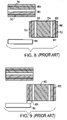
- the first mask is a dark field alternating phase shift mask 15 .
- the first mask includes intrusion pairs of zero degree and 180 degree phase-shifting regions 12 ′, 14 ′ respectively, and is used for making critical dimensioned exposure patterns on the wafer.
- the first mask 15 is opaque in all areas 13 except where the intrusion pairs 12 ′, 14 ′ are located.
- the second mask 16 is a bright field trim mask, which is transparent in all areas 17 except where block mask patterns 18 are present.
- the second mask 16 is used to expose the resist a second time after the resist is exposed using the first mask 15 . This technique is used with a positive resist in which exposed areas are developed away, leaving the unexposed areas to remain as the desired pattern.
- FIG. 2B illustrates a dark field altPSM mask 15 and FIG. 2D illustrates a block pattern of a bright field trim mask 16 corresponding thereto.
- FIGS. 2C and 2E illustrate corresponding patterns in the resist after lithographic exposure with the masks 2 B and 2 D, respectively. As illustrated in FIGS. 2C and 2E , the lithographic exposures have resulted in resist patterns 12 ′′, 14 ′′, and 17 ′ that have rounded corners instead of the original block shapes, due to the resolution limits described above.
- FIG. 2F shows the combined lithographic exposure pattern 10 ′ that results after exposure with the dark field altPSM mask 15 and another exposure with the bright field trim mask 16 . As illustrated in FIG. 2F , the resulting exposure 10 ′ reasonably approximates the desired pattern 10 of FIG. 2A .
- FIGS. 3A through 3D illustrate a sequence of steps performed in a prior art method of generating patterns of an altPSM mask and a block (trim) mask corresponding thereto.
- This process takes advantage of the constructive interference of light to double the achievable resolution of the optical lithography system.
- the light interference is created by selectively manipulating the topography of the photomask to introduce an appropriate path-length difference in the imaging light.
- FIG. 3A illustrates a transistor polysilicon shape 20 to be patterned by a dual exposure altPSM method.
- Each of the sample polysilicon shapes 20 reflects a shape similar to that of the desired transistor shape 10 shown in FIG. 2A , having a sub-cutoff dimension to be patterned by an altPSM mask having a pair of inverse phase-shifting regions 22 , 24 of zero degrees and 180 degrees phase shift on opposite sides of the transistor shape to be patterned.
- the phase shapes or regions need to obey a variety of lithographic, mask manufacturability, and design rules governing their size and spacings.
- the design of an altPSM layout requires that the inverse phase shifting shapes be located on opposing sides of the sub-cutoff dimension feature, such that one of the two inverse phase shapes is assigned a phase shift that is 180 degrees out of phase from that of the phase shape on the opposite side of the sub-cutoff dimension feature.
- both the zero degree phase shapes 22 and the 180 degree phase shapes 24 have to be defined as patterns in a data set representing the mask, even though no special processing is required to define zero degree phase shapes 22 in the mask.
- this figure is an illustration of a dark field alternating PSM layout.
- the sample polysilicon layout is still shown at 20 and the block mask 26 is illustrated by the crosshatched areas.
- the final exposure pattern will be formed in the photo-resist as the difference between the shadow cast by the block pattern 26 and the interference pattern produced by the zero degree and 180 degree phase shapes 22 , 24 respectively.
- FIGS. 3C and 3D An example of this is illustrated in FIGS. 3C and 3D .
- FIG. 3C an optimized altPSM layout is shown having phase extensions 30 (bottom of 180 degree portion) and phase end hammerheads 32 (top of 180 degree portion).
- phase extensions 30 bottom of 180 degree portion
- phase end hammerheads 32 top of 180 degree portion.
- This specific example is optimized to the situation where a gap between two primary features is filled with a common block shape being entirely covered by the block edge, and the phase edge is extended past its regular position.
- the top edge is not linearly extended, but hammerheads are added to counteract phase end shortening.
- FIG. 3D is a block mask similar to FIG. 3B .
- FIG. 4 illustrates process steps in the generation of phase shapes of an altPSM mask and block shapes of a corresponding block (trim) mask for use in a dual exposure method.
- design data for a circuit layout e.g. from a circuit design program
- step 102 all critical segments of the layout are identified.
- step 103 of creating basic phase shapes, i.e. the rough outlines of the polygons which will receive the phase information are defined.
- step 104 layout violations are removed from the generated phase shapes by a legalization process.
- Legalizing is the process of checking and adjusting or fixing patterns so that they conform to minimum space rules between features and minimum width rules, which are imposed by the lithography and mask manufacturing process.
- the phase regions are then colored (step 105 ).
- the shapes of the block mask are generated (step 106 ), and the block mask including those shapes is then legalized, in step 111 .
- a check is then made, in decision block 112 , to determine if the shapes of the phase-shifting mask are correctly adjusted for the shapes of the block mask that has just been generated. Very often, they are not, in which case, the result of the decision block 112 is “No”, and the process resumes again at step 104 with legalizing the shapes of the phase-shifting mask.
- new block shapes may be added when step 111 is encountered again to legalize the shapes of the block mask. Accordingly, the prior art method shown in FIG. 4 is a circular method in which the shapes of the block mask depend on the shapes of the phase-shifting mask, but the shapes of the phase-shifting mask also depend on the shapes of the block mask.
- a problem with the prior art method of FIG. 4 is the need to continually modify the layout by going back to the redefinition of critical segments. While the optimization altPSM parameters as provided above show great promise in improving lithographic performance, the circular definition of mask features challenges the capabilities of current tools to generate suitable altPSM and block mask combinations. As illustrated in FIG. 4 , the details of the phase shape design depend on critical layout segments, and the details of the block mask design depend on both critical layout segments and the exact phase design, but the exact phase design also depends on details of the block mask design.
- the present invention addresses these concerns by improving the parameter definition and design flow of generating altPSM mask and block mask pairs to generate lithographically optimized and logically correct altPSM layouts.
- FIGS. 5A through 11 illustrate steps in a prior art method for generating block patterns and phase-shifting patterns of a block (trim) mask and an altPSM mask for use in a dual exposure method for defining critical dimensioned features in a resist pattern of a substrate.
- a feature 401 and critical dimensioned features 402 of a circuit layout are identified according to step 102 of the method shown in FIG. 4 .
- a set of phase regions 502 are then generated for the phase shifting mask, the phase regions 502 lying on each side of the critical dimensioned features 504 to be patterned.
- the phase regions are legalized, resulting in one larger phase region 602 , as shown in FIG. 6 , because the prior spacing between the phase regions 502 did not conform to rules for minimum spacing between adjacent phase regions.
- a step of coloring the legalized phase regions is conducted, as shown in FIG. 7 , in that the shapes 702 are assigned zero degree phase and shapes 704 are assigned 180 degree phase.
- the shapes of the block mask are designed. Since, as illustrated in FIG.
- the function of the block mask patterns in this double exposure altPSM technique is twofold: 1) to cover and protect shapes patterned by the phase mask; and 2) to image non-critical shapes that are not being patterned by the phase mask, the block mask consists of two types of patterns, one where the block mask is coincident with non-critical patterns, 806 , the other where the block pattern 802 , 804 extends beyond the side-edges of critical shapes 801 but stops short of the edges of the phase shapes, 702 , 704 .
- the block mask shapes are now legalized, such that the pattern of block shapes are checked for conformity with rules regarding minimum block shape width and minimum spacing between block shapes.
- the mask rule requires that the subminimum width space between them be filled with another block shape. This result is illustrated in FIG. 9 by the addition of the block shape 901 between the block shapes 902 and 903 .
- the shapes of the phase mask are now adjusted relative to the block mask shapes that have been created, such that certain of the phase shapes are now enlarged in this step.
- the shapes 1001 and 1002 which extend outside the block shape 1006 are now added to counteract phase-end shortening when the masks are used to print the critical dimensioned features 1008 , and a phase shape 1004 at zero degree phase is added which adjoins the existing zero degree phase shape 1003 in the location of the added block mask shape 1010 .
- step 104 of the method illustrated in FIG. 4 As shown in FIG. 11 , this step now results in a new shape 1102 being added between the shapes 1104 and 1106 of the phase mask, where minimum spacing did not exist before between those shapes 1104 and 1106 .
- the present invention provides a method and apparatus of generating mask patterns for an alternating phase shift mask, in which block-mask patterns are generated first, based on critical segments of the primary layout, not based on the phase mask pattern design. Thereafter, the phase mask patterns are derived from the block mask patterns as well as the critical segments of the primary circuit layout.
- a method of generating patterns of a paired set of photomasks from a data set defining a circuit layout to be provided on a substrate includes identifying critical segments of the circuit layout to be provided on the substrate. Block mask patterns are generated and then legalized based on the identified critical segments. Thereafter, phase mask patterns are generated, legalized and colored.
- the legalized block mask patterns and the legalized and colored phase mask patterns define features of a block mask and an alternating phase shift mask, respectively, for use in a dual exposure method for patterning features in a resist layer of a substrate.
- FIG. 1A illustrates principles of optical lithography.
- FIGS. 1B and 1C illustrate two-beam imaging principles in alternating phase-shift mask lithography.
- FIGS. 2A through 2F illustrate steps in the performance of a dual exposure altPSM method using a dark field phase-shift mask and a bright field block (trim) mask.
- FIGS. 3A through 3D illustrate sequences in a prior art method of generating phase-shifting shapes and block shapes for inclusion in an altPSM mask and a block (trim) mask used therewith in a dual exposure altPSM lithography method.
- FIG. 4 is a flowchart illustrating steps performed in a prior art method to generate phase-shifting shapes and block shapes for inclusion in an altPSM mask and a block (trim) mask used therewith in a dual exposure altPSM lithography method.
- FIGS. 5A–11 illustrate sequences of generating shapes of a phase-shifting mask and shapes of a block mask according to the method illustrated in FIG. 4 .
- FIG. 12 is a flowchart illustrating steps performed in an embodiment of the invention to generate phase-shifting shapes and block shapes for inclusion in an altPSM mask and a block (trim) mask used therewith in a dual exposure altPSM lithography method.
- FIGS. 13–18 illustrate sequences of generating shapes of a phase-shifting mask and shapes of a block mask, according to the method illustrated in FIG. 12 .
- FIG. 19 is a diagram of a system embodiment of the invention operable to generate phase-shifting shapes and block shapes for inclusion in an altPSM mask and a block (trim) mask used therewith in a dual exposure altPSM lithography method.
- FIG. 12 is a flowchart illustrating an embodiment of the present invention.
- an approach is provided for defining all parameters of the block (trim) mask only as a function of the primary circuit layout. Thereafter, parameters of the phase shape patterns are defined as a function of both the primary circuit layout, as well as the block mask patterns.
- steps for generating phase-shift mask patterns and block mask patterns are performed in the reverse order from those performed according to the prior art method shown in FIG. 4 .
- steps of the method of the embodiment shown in FIGS. 12–18 will be compared to the steps of the prior art method, as described above relative to FIGS. 4 through 11 .
- the mask generation process begins with the inputting ( 1201 ) of a circuit layout and identification ( 1202 ) of the critical segments of the circuit layout.
- Critical segments are those segments of the layout which have critical dimensions, e.g. at or below the cutoff dimension of the lithography system being used.
- Critical segments are shown in FIG. 13 as the segments 1301 having narrow width that is below the cutoff dimension, i.e., smaller than can be photolithographically defined using only a block mask pattern.
- This step is then followed by the step ( 1206 ) of designing the block mask, i.e., designing the mask shapes 1401 and 1402 of the block mask, as shown in FIG. 14 .
- These appear as the larger shapes 1401 corresponding to and surrounding each of the identified critical segments 1301 , shown for reference, as well as the shape 1402 which surrounds the non-critical segment.
- This step ( 1206 ) differs from the prior art method in that it is performed prior to generation of the phase regions of the altPSM mask, and it is performed based only on the critical segments of the circuit layout that have been identified.
- the prior art method by contrast, performed the step of generating block mask patterns after generating the phase regions, and did so based on both the critical segments of the layout and the shapes of the already generated phase mask design.
- the next step in the method is to legalize ( 1207 ) the block mask patterns, as shown in FIG. 15 .
- the block mask shapes are checked for conformity with rules that require that each block mask shape to have a minimum width and that a minimum space be provided between neighboring block shapes.
- block mask shapes 1501 and 1504 remain unchanged as they already conform to these rules.
- block mask shape 1502 is enlarged, because, before that time, the spacing between block mask shapes was less than the minimum width.
- a new block mask shape 1503 is generated to fill the subminimum dimension that is not permitted to exist between the shapes 1502 and 1504 .
- phase regions 1601 – 1605 of the altPSM mask are generated (step 1203 ).
- the phase regions define the locations where mask shapes having alternating phases are to be located.
- the actual amount of phase shift and the locations of phase-shifting elements are not determined until a coloring step that occurs after the dimensions of the phase regions are determined.
- phase regions are legalized (step 1204 ) such that they are made to conform to rules regarding the minimum width of phase regions and the minimum spacing between adjacent phase regions.
- an additional phase region 1701 is added between the phase regions 1702 and 1705 that existed from the previous step of generating the phase regions ( FIG. 16 ).
- the additional phase region 1701 compensates for unwanted interaction between the phase regions 1702 and 1705 that are closer than the minimum spacing defined by the rule.
- the generation and legalization of the phase regions are followed by the step ( 1205 ) of coloring the phase regions, i.e. designating the particular phase shift to be applied to particular phase regions of the altPSM mask.
- the phase regions 1801 are colored with a phase shift of zero degrees and other phase regions 1802 between the phase regions 1801 are colored with a phase shift of 180 degrees.
- FIGS. 12 through 18 provides clear advantages over the prior art methods described above. Comparing the embodiment to the prior art method in the sequence of steps that are performed, it is clear that the method of the embodiment provides advantages. After coloring the phase regions, all of the block mask shapes of the trim mask have already been determined, and all of the phase-shifting regions of the altPSM mask and their coloring has been determined. Therefore, the last step ( 1209 ) of the method is to derive the data that represents all of the block mask shapes and phase-shifting region shapes for driving a mask patterning tool to fabricate the respective bright field block trim mask and dark field altPSM mask.
- the embodiment of the invention differs here from the prior art method in that after the phase regions have been generated, legalized and colored, processing can generally proceed to deriving the final mask data, without requiring further checking or adjustments of the block mask shapes or the block mask shapes to be made in relation to the phase mask shapes.
- the flow of generating both block mask shapes of the trim mask and the phase-shifting shapes of the altPSM mask is linear, not requiring the method to loop back iteratively, thereby saving much time and processing resources in generating the patterns of the masks.
- the method of the embodiment of the invention described herein generates mask patterns which are as accurate, if not even more accurate, than the mask patterns which are generated using the prior art methods described in the background section above.
- reversing the order of the generation of block mask shapes and phase-shifting shapes yields a lithographically optimized and logically correct altPSM layout.
- This improved method of generating mask patterns can be implemented to simplify the production of masks not only for producing VLSI-CMOS logic chips, but for implementing hierarchical shapes and manipulation tools that are used for memory circuits, preferably those designed to a groundrule of 90 nm or less, logic circuits, or other similar devices.
- the present invention also provides for a mechanism to provide such modification.
- the method of the present invention provides either a more accurate design or a design with the same degree of accuracy but at an earlier stage in processing, as compared to that provided by the prior art methods.
- the programs by which the methods are implemented can be stored in one or more types of machine-readable media that are suited to transporting the program from one location to another.
- FIG. 19 illustrates another embodiment of the invention in which a system is operable to produce patterns of a block mask and patterns of a phase-shifting mask according to the invention.
- the system includes a processor 2004 including a central processor unit (CPU) 2001 and a memory (MEM) 2003 , and an input output interface (IO) 2005 , through which instructions and data input are received, and through which data output is transmitted.
- the memory can include only cache storage in the CPU, or it preferably includes additional memory, such as a main memory outside of the CPU, which may include only integrated circuit memory, or disk or tape drive media.
- the input output interface IO 2005 is operable to receive data ( 2007 ) representing a circuit layout to be provided on a substrate.
- the processor 2004 is operable to identify critical segments of the circuit layout, and to generate and legalize block mask patterns based on the identified critical segments.
- the processor 2004 is further operable to generate and legalize phase mask patterns for use in conjunction with the legalized block mask patterns to produce masks which define an exposure pattern on the substrate.
- the processor is further operable to color the phase mask patterns to appropriate phases.
- the processor then outputs ( 2009 ) a data set through the IO 2005 which defines the patterns to be inscribed on a block mask and the patterns to be inscribed on a phase mask for a pair of a phase mask and a block (trim) mask for use according to a dual exposure altPSM technique.
Abstract
Description
sin θ=mλ/P (1)
P min =λ/NA (2)
R min=0.5λ/NA (3)
R=k 1 λ/NA (4)
k 1=Dimension (NA/λ) (5)
ΔPL=z−z cos θ (6)
DOF=(λ/4)(1/(1−cos θ)) (7)
DOF=λ/(2NA 2) (8)
| TABLE 1 | ||||||
| Intended | Year of | |||||
| Source | λ (nm) | λ ratio | Resolution | Introd. | ||
| G-line | 436 | micron | ||||
| I-line | 365 | .83 | half-micron | 1984 | ||
| KrF | 248 | .68 | quarter- | 1989 | ||
| micron | ||||||
| ArF | 193 | .78 | 100 nm- | 2001 | ||
| node | ||||||
| F2 | 157 | .81 | 65 nm-node | Expect | ||
| 2004 | ||||||
| Ar2 | 126 | .80 | 45 nm-node | * | ||
| Lithography wavelengths and their applicability, | ||||||
| *126 nm lithography is no longer considered a viable option. | ||||||
| TABLE 2 | ||||||
| ITRS | Man. | Min. | ||||
| Node | Year | Pitch | Dev. λ/NA | Man. λ/NA | Dev. k1 | Man. |
| 180 | 1999 | 500 | 248/.50 | 248/.75 | .50 | .76 |
| 130 | 2001 | 300 | 248/.75 | 193/.75 | .45 | .58 |
| 90 | 2003 | 214 | 193/.75 | 193/.85 | .42 | .48 |
| 65 | 2005 | 160 | 193/.85 | 157/.85* | .35 | (.43) |
| 45 | 2007 | 130 | 157/.85* | Unknown | (.35) | Unknown |
| λ/NA solutions for recent technology nodes [1], illustrating the constant erosion of k1 for both technology development (Dev.) and manufacturing (Man.) | ||||||
| *Potential Solution | ||||||
R=0.25λ/NA (9)
Etch Depth=0.5λ/(n−1) (10)
Claims (14)
Priority Applications (3)
| Application Number | Priority Date | Filing Date | Title |
|---|---|---|---|
| US10/604,373 US6993741B2 (en) | 2003-07-15 | 2003-07-15 | Generating mask patterns for alternating phase-shift mask lithography |
| JP2004207387A JP4019072B2 (en) | 2003-07-15 | 2004-07-14 | Alternating phase shift mask lithography mask pattern generation |
| US11/318,893 US7475380B2 (en) | 2003-07-15 | 2005-12-27 | Generating mask patterns for alternating phase-shift mask lithography |
Applications Claiming Priority (1)
| Application Number | Priority Date | Filing Date | Title |
|---|---|---|---|
| US10/604,373 US6993741B2 (en) | 2003-07-15 | 2003-07-15 | Generating mask patterns for alternating phase-shift mask lithography |
Related Child Applications (1)
| Application Number | Title | Priority Date | Filing Date |
|---|---|---|---|
| US11/318,893 Continuation US7475380B2 (en) | 2003-07-15 | 2005-12-27 | Generating mask patterns for alternating phase-shift mask lithography |
Publications (2)
| Publication Number | Publication Date |
|---|---|
| US20050014074A1 US20050014074A1 (en) | 2005-01-20 |
| US6993741B2 true US6993741B2 (en) | 2006-01-31 |
Family
ID=34062246
Family Applications (2)
| Application Number | Title | Priority Date | Filing Date |
|---|---|---|---|
| US10/604,373 Expired - Fee Related US6993741B2 (en) | 2003-07-15 | 2003-07-15 | Generating mask patterns for alternating phase-shift mask lithography |
| US11/318,893 Expired - Fee Related US7475380B2 (en) | 2003-07-15 | 2005-12-27 | Generating mask patterns for alternating phase-shift mask lithography |
Family Applications After (1)
| Application Number | Title | Priority Date | Filing Date |
|---|---|---|---|
| US11/318,893 Expired - Fee Related US7475380B2 (en) | 2003-07-15 | 2005-12-27 | Generating mask patterns for alternating phase-shift mask lithography |
Country Status (2)
| Country | Link |
|---|---|
| US (2) | US6993741B2 (en) |
| JP (1) | JP4019072B2 (en) |
Cited By (40)
| Publication number | Priority date | Publication date | Assignee | Title |
|---|---|---|---|---|
| US20050153215A1 (en) * | 2004-01-13 | 2005-07-14 | International Business Machines Corporation | Real-time configurable masking |
| US20060156270A1 (en) * | 2005-01-10 | 2006-07-13 | Melvin Lawrence S Iii | Method and apparatus for correcting 3D mask effects |
| US20070006113A1 (en) * | 2005-06-30 | 2007-01-04 | Bin Hu | Determining an optimizaton for generating a pixelated photolithography mask with high resolution imaging capability |
| US20070275310A1 (en) * | 2006-05-26 | 2007-11-29 | Yasushi Tanaka | Method for determining an acceptable reticle tolerance for a reticle used to produce an integrated circuit layout |
| US20090004573A1 (en) * | 2007-06-29 | 2009-01-01 | Aton Thomas J | System and method for making photomasks |
| US20090014811A1 (en) * | 2006-03-09 | 2009-01-15 | Tela Innovations, Inc. | Dynamic Array Architecture |
| US20090032898A1 (en) * | 2007-08-02 | 2009-02-05 | Tela Innovations, Inc. | Methods for Defining Dynamic Array Section with Manufacturing Assurance Halo and Apparatus Implementing the Same |
| US20090100396A1 (en) * | 2007-02-20 | 2009-04-16 | Tela Innovations, Inc. | Methods and Systems for Process Compensation Technique Acceleration |
| US20090128788A1 (en) * | 2007-06-29 | 2009-05-21 | Aton Thomas J | System and method for making photomasks |
| US20090152734A1 (en) * | 2007-12-13 | 2009-06-18 | Tela Innovations, Inc. | Super-Self-Aligned Contacts and Method for Making the Same |
| US20090224396A1 (en) * | 2006-03-09 | 2009-09-10 | Becker Scott T | Oversized Contacts and Vias in Semiconductor Chip Defined by Linearly Constrained Topology |
| US20090228853A1 (en) * | 2006-03-09 | 2009-09-10 | Tela Innovations, Inc. | Methods for Defining Contact Grid in Dynamic Array Architecture |
| US20090224408A1 (en) * | 2008-03-27 | 2009-09-10 | Tela Innovations, Inc. | Methods for Multi-Wire Routing and Apparatus Implementing Same |
| US20090224317A1 (en) * | 2008-03-13 | 2009-09-10 | Tela Innovations, Inc. | Cross-Coupled Transistor Layouts in Restricted Gate Level Layout Architecture |
| US20090228857A1 (en) * | 2008-01-31 | 2009-09-10 | Tela Innovations, Inc. | Enforcement of Semiconductor Structure Regularity for Localized Transistors and Interconnect |
| US20090271753A1 (en) * | 2007-08-02 | 2009-10-29 | Tela Innovations. Inc. | Methods for Cell Phasing and Placement in Dynamic Array Architecture and Implementation of the Same |
| US20090283915A1 (en) * | 2006-03-09 | 2009-11-19 | Becker Scott T | Oversized Contacts and Vias in Layout Defined by Linearly Constrained Topology |
| US20090300575A1 (en) * | 2006-03-09 | 2009-12-03 | Stephen Kornachuk | Optimizing Layout of Irregular Structures in Regular Layout Context |
| US20090294981A1 (en) * | 2006-03-09 | 2009-12-03 | Tela Innovations, Inc. | Methods for Defining and Using Co-Optimized Nanopatterns for Integrated Circuit Design and Apparatus Implementing Same |
| US20090300574A1 (en) * | 2006-03-09 | 2009-12-03 | Brian Reed | Methods for Defining and Utilizing Sub-Resolution Features in Linear Topology |
| US20100006901A1 (en) * | 2006-03-09 | 2010-01-14 | Tela Innovations, Inc. | Semiconductor Device Portion Having Gate Electrode Conductive Structures Formed from Rectangular Shaped Gate Electrode Layout Features Defined Along At Least Four Gate Electrode Tracks and Having Corresponding Non-Symmetric Diffusion Regions |
| US20100023917A1 (en) * | 2003-02-25 | 2010-01-28 | The Regents Of The University Of California | Tool for modifying mask design layout |
| US20100031211A1 (en) * | 2008-08-01 | 2010-02-04 | Tela Innovations, Inc. | Methods for Controlling Microloading Variation in Semiconductor Wafer Layout and Fabrication |
| US7730432B1 (en) | 2005-03-30 | 2010-06-01 | Tela Innovations, Inc. | Method and system for reshaping a transistor gate in an integrated circuit to achieve a target objective |
| US20100169847A1 (en) * | 2005-05-06 | 2010-07-01 | Tela Innovations. Inc., A Delaware Corporation | Standard cells having transistors annotated for gate-length biasing |
| US20100169846A1 (en) * | 2005-05-06 | 2010-07-01 | Tela Innovations. Inc., A Delaware Corporation | Methods for gate-length biasing using annotation data |
| US20100252896A1 (en) * | 2007-10-26 | 2010-10-07 | Tela Innovations, Inc. | Methods, Structures, and Designs for Self-Aligning Local Interconnects used in Integrated Circuits |
| US20100277202A1 (en) * | 2006-03-09 | 2010-11-04 | Tela Innovations, Inc. | Circuitry and Layouts for XOR and XNOR Logic |
| US20100287518A1 (en) * | 2009-05-06 | 2010-11-11 | Tela Innovations, Inc. | Cell Circuit and Layout with Linear Finfet Structures |
| US20110084312A1 (en) * | 2009-10-13 | 2011-04-14 | Tela Innovations, Inc. | Methods for Cell Boundary Encroachment and Layouts Implementing the Same |
| US7932545B2 (en) | 2006-03-09 | 2011-04-26 | Tela Innovations, Inc. | Semiconductor device and associated layouts including gate electrode level region having arrangement of six linear conductive segments with side-to-side spacing less than 360 nanometers |
| US7979829B2 (en) | 2007-02-20 | 2011-07-12 | Tela Innovations, Inc. | Integrated circuit cell library with cell-level process compensation technique (PCT) application and associated methods |
| US20120094492A1 (en) * | 2010-10-13 | 2012-04-19 | Dong-Woon Park | Method of forming pattern, reticle, and computer readable medium for storing program for forming pattern |
| US8658542B2 (en) | 2006-03-09 | 2014-02-25 | Tela Innovations, Inc. | Coarse grid design methods and structures |
| US8667443B2 (en) | 2007-03-05 | 2014-03-04 | Tela Innovations, Inc. | Integrated circuit cell library for multiple patterning |
| US8839175B2 (en) | 2006-03-09 | 2014-09-16 | Tela Innovations, Inc. | Scalable meta-data objects |
| US8863063B2 (en) | 2009-05-06 | 2014-10-14 | Tela Innovations, Inc. | Finfet transistor circuit |
| US9035359B2 (en) | 2006-03-09 | 2015-05-19 | Tela Innovations, Inc. | Semiconductor chip including region including linear-shaped conductive structures forming gate electrodes and having electrical connection areas arranged relative to inner region between transistors of different types and associated methods |
| US9159627B2 (en) | 2010-11-12 | 2015-10-13 | Tela Innovations, Inc. | Methods for linewidth modification and apparatus implementing the same |
| US10216890B2 (en) | 2004-04-21 | 2019-02-26 | Iym Technologies Llc | Integrated circuits having in-situ constraints |
Families Citing this family (12)
| Publication number | Priority date | Publication date | Assignee | Title |
|---|---|---|---|---|
| US7234128B2 (en) * | 2003-10-03 | 2007-06-19 | Taiwan Semiconductor Manufacturing Company, Ltd. | Method for improving the critical dimension uniformity of patterned features on wafers |
| US20050112474A1 (en) * | 2003-11-20 | 2005-05-26 | Micronic Laser Systems Ab | Method involving a mask or a reticle |
| US7111276B2 (en) * | 2004-02-05 | 2006-09-19 | Synopsys, Inc. | Correcting 3D effects in phase shifting masks using sub-resolution features |
| US7560197B2 (en) * | 2004-02-23 | 2009-07-14 | Kabushiki Kaisha Toshiba | Mask pattern data producing method, patterning method, reticle correcting method, reticle manufacturing method, and semiconductor apparatus manufacturing method |
| US20060257749A1 (en) * | 2005-05-16 | 2006-11-16 | Sheng-Yueh Chang | Method for reducing critical dimension |
| US7650587B2 (en) * | 2006-11-30 | 2010-01-19 | International Business Machines Corporation | Local coloring for hierarchical OPC |
| JP4909729B2 (en) * | 2006-12-13 | 2012-04-04 | 株式会社東芝 | Inspection data creation method and inspection method |
| JP4779003B2 (en) * | 2007-11-13 | 2011-09-21 | エーエスエムエル ネザーランズ ビー.ブイ. | Method for pattern decomposition of full chip designs |
| US8082525B2 (en) * | 2008-04-15 | 2011-12-20 | Luminescent Technologies, Inc. | Technique for correcting hotspots in mask patterns and write patterns |
| US8219939B2 (en) * | 2009-11-12 | 2012-07-10 | Advanced Micro Devices, Inc. | Method of creating photolithographic masks for semiconductor device features with reduced design rule violations |
| US8429574B2 (en) * | 2011-04-14 | 2013-04-23 | Cadence Design Systems, Inc. | Dual-pattern coloring technique for mask design |
| KR102224518B1 (en) * | 2013-06-24 | 2021-03-08 | 삼성전자주식회사 | Double patterning layout design method |
Citations (20)
| Publication number | Priority date | Publication date | Assignee | Title |
|---|---|---|---|---|
| US5807649A (en) | 1996-10-31 | 1998-09-15 | International Business Machines Corporation | Lithographic patterning method and mask set therefor with light field trim mask |
| US5883813A (en) * | 1997-03-04 | 1999-03-16 | International Business Machines Corporation | Automatic generation of phase shift masks using net coloring |
| US6258493B1 (en) | 1996-09-18 | 2001-07-10 | Numerical Technologies, Inc. | Phase shifting circuit manufacture method and apparatus |
| US6338922B1 (en) | 2000-05-08 | 2002-01-15 | International Business Machines Corporation | Optimized alternating phase shifted mask design |
| US20020045136A1 (en) | 2000-09-13 | 2002-04-18 | Michael Fritze | Method of design and fabrication of integrated circuits using regular arrays and gratings |
| US20020046392A1 (en) * | 2000-10-16 | 2002-04-18 | Burkhard Ludwig | Method for detecting and automatically eliminating phase conflicts on alternating phase masks |
| US20020071997A1 (en) | 2000-08-31 | 2002-06-13 | Infineon Techonologies Ag | OPC method for generating corrected patterns for a phase-shifting mask and its trimming mask and associated device and integrated circuit configuration |
| US20020081500A1 (en) | 1999-09-28 | 2002-06-27 | Cobb Nicolas Bailey | Method and apparatus for determining phase shifts and trim masks for an integrated circuit |
| US20020083410A1 (en) | 2000-10-25 | 2002-06-27 | Numerical Technologies, Inc. | Resolving phase-shift conflicts in layouts using weighted links between phase shifters |
| US20020094492A1 (en) | 1999-12-17 | 2002-07-18 | Randall John N. | Two-exposure phase shift photolithography with improved inter-feature separation |
| US6493866B1 (en) * | 2000-06-30 | 2002-12-10 | Synopsys, Inc. | Phase-shift lithography mapping and apparatus |
| US20030014732A1 (en) * | 2001-07-13 | 2003-01-16 | Numerical Technologies, Inc. | Alternating phase shift mask design conflict resolution |
| US20030070155A1 (en) * | 2001-10-09 | 2003-04-10 | Numerical Technologies, Inc. | Method and apparatus for resolving coloring conflicts between phase shifters |
| US20030229879A1 (en) * | 2002-06-11 | 2003-12-11 | Numerical Technologies, Inc. | Model-based data conversion |
| US6721938B2 (en) * | 2001-06-08 | 2004-04-13 | Numerical Technologies, Inc. | Optical proximity correction for phase shifting photolithographic masks |
| US6733929B2 (en) * | 2000-07-05 | 2004-05-11 | Numerical Technologies, Inc. | Phase shift masking for complex patterns with proximity adjustments |
| US6823503B2 (en) * | 2002-12-31 | 2004-11-23 | Numerical Technologies, Inc. | Method and apparatus for creating a phase-shifting mask for a photolithographic process |
| US6846596B2 (en) * | 2001-03-08 | 2005-01-25 | Numerical Technologies, Inc. | Alternating phase shift masking for multiple levels of masking resolution |
| US20050081178A1 (en) * | 2003-10-08 | 2005-04-14 | Sivakumar Swaminathan (Sam) | Multiple exposure technique to pattern tight contact geometries |
| US6904587B2 (en) * | 2002-12-20 | 2005-06-07 | Synopsys, Inc. | Incremental lithography mask layout design and verification |
Family Cites Families (1)
| Publication number | Priority date | Publication date | Assignee | Title |
|---|---|---|---|---|
| US5858580A (en) * | 1997-09-17 | 1999-01-12 | Numerical Technologies, Inc. | Phase shifting circuit manufacture method and apparatus |
-
2003
- 2003-07-15 US US10/604,373 patent/US6993741B2/en not_active Expired - Fee Related
-
2004
- 2004-07-14 JP JP2004207387A patent/JP4019072B2/en not_active Expired - Fee Related
-
2005
- 2005-12-27 US US11/318,893 patent/US7475380B2/en not_active Expired - Fee Related
Patent Citations (21)
| Publication number | Priority date | Publication date | Assignee | Title |
|---|---|---|---|---|
| US6258493B1 (en) | 1996-09-18 | 2001-07-10 | Numerical Technologies, Inc. | Phase shifting circuit manufacture method and apparatus |
| US20010028985A1 (en) | 1996-09-18 | 2001-10-11 | Yao-Ting Wang | Phase shifting circuit manufacture method and apparatus |
| US5807649A (en) | 1996-10-31 | 1998-09-15 | International Business Machines Corporation | Lithographic patterning method and mask set therefor with light field trim mask |
| US5883813A (en) * | 1997-03-04 | 1999-03-16 | International Business Machines Corporation | Automatic generation of phase shift masks using net coloring |
| US20020081500A1 (en) | 1999-09-28 | 2002-06-27 | Cobb Nicolas Bailey | Method and apparatus for determining phase shifts and trim masks for an integrated circuit |
| US20020094492A1 (en) | 1999-12-17 | 2002-07-18 | Randall John N. | Two-exposure phase shift photolithography with improved inter-feature separation |
| US6338922B1 (en) | 2000-05-08 | 2002-01-15 | International Business Machines Corporation | Optimized alternating phase shifted mask design |
| US6493866B1 (en) * | 2000-06-30 | 2002-12-10 | Synopsys, Inc. | Phase-shift lithography mapping and apparatus |
| US6733929B2 (en) * | 2000-07-05 | 2004-05-11 | Numerical Technologies, Inc. | Phase shift masking for complex patterns with proximity adjustments |
| US20020071997A1 (en) | 2000-08-31 | 2002-06-13 | Infineon Techonologies Ag | OPC method for generating corrected patterns for a phase-shifting mask and its trimming mask and associated device and integrated circuit configuration |
| US20020045136A1 (en) | 2000-09-13 | 2002-04-18 | Michael Fritze | Method of design and fabrication of integrated circuits using regular arrays and gratings |
| US20020046392A1 (en) * | 2000-10-16 | 2002-04-18 | Burkhard Ludwig | Method for detecting and automatically eliminating phase conflicts on alternating phase masks |
| US20020083410A1 (en) | 2000-10-25 | 2002-06-27 | Numerical Technologies, Inc. | Resolving phase-shift conflicts in layouts using weighted links between phase shifters |
| US6846596B2 (en) * | 2001-03-08 | 2005-01-25 | Numerical Technologies, Inc. | Alternating phase shift masking for multiple levels of masking resolution |
| US6721938B2 (en) * | 2001-06-08 | 2004-04-13 | Numerical Technologies, Inc. | Optical proximity correction for phase shifting photolithographic masks |
| US20030014732A1 (en) * | 2001-07-13 | 2003-01-16 | Numerical Technologies, Inc. | Alternating phase shift mask design conflict resolution |
| US20030070155A1 (en) * | 2001-10-09 | 2003-04-10 | Numerical Technologies, Inc. | Method and apparatus for resolving coloring conflicts between phase shifters |
| US20030229879A1 (en) * | 2002-06-11 | 2003-12-11 | Numerical Technologies, Inc. | Model-based data conversion |
| US6904587B2 (en) * | 2002-12-20 | 2005-06-07 | Synopsys, Inc. | Incremental lithography mask layout design and verification |
| US6823503B2 (en) * | 2002-12-31 | 2004-11-23 | Numerical Technologies, Inc. | Method and apparatus for creating a phase-shifting mask for a photolithographic process |
| US20050081178A1 (en) * | 2003-10-08 | 2005-04-14 | Sivakumar Swaminathan (Sam) | Multiple exposure technique to pattern tight contact geometries |
Non-Patent Citations (1)
| Title |
|---|
| Sewell,H et al. "An Evaluation of the Dual Exposure Technique", Proceedings of the SPIE-The International Society for Optical Engineering, vol. 4344, pp. 323-333, 2001. * |
Cited By (313)
| Publication number | Priority date | Publication date | Assignee | Title |
|---|---|---|---|---|
| US8103981B2 (en) | 2003-02-25 | 2012-01-24 | The Regents Of The University Of California | Tool for modifying mask design layout |
| US20100023917A1 (en) * | 2003-02-25 | 2010-01-28 | The Regents Of The University Of California | Tool for modifying mask design layout |
| US7361457B2 (en) * | 2004-01-13 | 2008-04-22 | International Business Machines Corporation | Real-time configurable masking |
| US20050153215A1 (en) * | 2004-01-13 | 2005-07-14 | International Business Machines Corporation | Real-time configurable masking |
| US10846454B2 (en) | 2004-04-21 | 2020-11-24 | Iym Technologies Llc | Integrated circuits having in-situ constraints |
| US10860773B2 (en) | 2004-04-21 | 2020-12-08 | Iym Technologies Llc | Integrated circuits having in-situ constraints |
| US10216890B2 (en) | 2004-04-21 | 2019-02-26 | Iym Technologies Llc | Integrated circuits having in-situ constraints |
| US20060156270A1 (en) * | 2005-01-10 | 2006-07-13 | Melvin Lawrence S Iii | Method and apparatus for correcting 3D mask effects |
| US7308673B2 (en) * | 2005-01-10 | 2007-12-11 | Synopsys, Inc. | Method and apparatus for correcting 3D mask effects |
| US7730432B1 (en) | 2005-03-30 | 2010-06-01 | Tela Innovations, Inc. | Method and system for reshaping a transistor gate in an integrated circuit to achieve a target objective |
| US8490043B2 (en) | 2005-05-06 | 2013-07-16 | Tela Innovations, Inc. | Standard cells having transistors annotated for gate-length biasing |
| US9202003B2 (en) | 2005-05-06 | 2015-12-01 | Tela Innovations, Inc. | Gate-length biasing for digital circuit optimization |
| US8185865B2 (en) | 2005-05-06 | 2012-05-22 | Tela Innovations, Inc. | Methods for gate-length biasing using annotation data |
| US8127266B1 (en) | 2005-05-06 | 2012-02-28 | Tela Innovations, Inc. | Gate-length biasing for digital circuit optimization |
| US9069926B2 (en) | 2005-05-06 | 2015-06-30 | Tela Innovations, Inc. | Standard cells having transistors annotated for gate-length biasing |
| US8756555B2 (en) | 2005-05-06 | 2014-06-17 | Tela Innovations, Inc. | Standard cells having transistors annotated for gate-length biasing |
| US8949768B2 (en) | 2005-05-06 | 2015-02-03 | Tela Innovations, Inc. | Standard cells having transistors annotated for gate-length biasing |
| US8869094B2 (en) | 2005-05-06 | 2014-10-21 | Tela Innovations, Inc. | Standard cells having transistors annotated for gate-length biasing |
| US20100169846A1 (en) * | 2005-05-06 | 2010-07-01 | Tela Innovations. Inc., A Delaware Corporation | Methods for gate-length biasing using annotation data |
| US20100169847A1 (en) * | 2005-05-06 | 2010-07-01 | Tela Innovations. Inc., A Delaware Corporation | Standard cells having transistors annotated for gate-length biasing |
| US8635583B2 (en) | 2005-05-06 | 2014-01-21 | Tela Innovations, Inc. | Standard cells having transistors annotated for gate-length biasing |
| US20070006113A1 (en) * | 2005-06-30 | 2007-01-04 | Bin Hu | Determining an optimizaton for generating a pixelated photolithography mask with high resolution imaging capability |
| US7923757B2 (en) | 2006-03-09 | 2011-04-12 | Tela Innovations, Inc. | Semiconductor device and associated layouts having linear shaped gate electrodes defined along at least five adjacent gate electrode tracks of equal pitch with gate electrode connection through single interconnect level |
| US20100017768A1 (en) * | 2006-03-09 | 2010-01-21 | Tela Innovations, Inc. | Layout of Cell of Semiconductor Device Having Rectangular Shaped Gate Electrode Layout Features Defined Along At Least Four Gate Electrode Tracks with Corresponding p-type and n-type Diffusion Regions Separated by Central Inactive Region |
| US20100011330A1 (en) * | 2006-03-09 | 2010-01-14 | Tela Innovations, Inc. | Semiconductor Device Layout Having Restricted Layout Region Including Linear Shaped Gate Electrode Layout Features Defined Along At Least Four Gate Electrode Tracks with Minimum End-to-End Spacing with Corresponding Non-Symmetric Diffusion Regions |
| US20100006950A1 (en) * | 2006-03-09 | 2010-01-14 | Tela Innovations, Inc. | Semiconductor Device Portion Having Gate Electrode Conductive Structures Formed from Rectangular Shaped Gate Electrode Layout Features and Having At Least Eight Transistors |
| US20100006901A1 (en) * | 2006-03-09 | 2010-01-14 | Tela Innovations, Inc. | Semiconductor Device Portion Having Gate Electrode Conductive Structures Formed from Rectangular Shaped Gate Electrode Layout Features Defined Along At Least Four Gate Electrode Tracks and Having Corresponding Non-Symmetric Diffusion Regions |
| US7952119B2 (en) | 2006-03-09 | 2011-05-31 | Tela Innovations, Inc. | Semiconductor device and associated layout having three or more linear-shaped gate electrode level conductive segments of both equal length and equal pitch |
| US20100006948A1 (en) * | 2006-03-09 | 2010-01-14 | Tela Innovations, Inc. | Semiconductor Device Portion Having Sub-193 Nanometers -Sized Gate Electrode Conductive Structures Formed from Rectangular Shaped Gate Electrode Layout Features and Having At Least Eight Transistors |
| US20100006947A1 (en) * | 2006-03-09 | 2010-01-14 | Tela Innovations, Inc. | Semiconductor Device Portion Having Sub-Wavelength-Sized Gate Electrode Conductive Structures Formed from Rectangular Shaped Gate Electrode Layout Features and Having At Least Eight Transistors |
| US20100006902A1 (en) * | 2006-03-09 | 2010-01-14 | Tela Innovations, Inc. | Semiconductor Device Portion Having Sub-Wavelength-Sized Gate Electrode Conductive Structures Formed from Rectangular Shaped Gate Electrode Layout Features Defined Along At Least Four Gate Electrode Tracks and Having Corresponding Non-Symmetric Diffusion Regions |
| US20100011329A1 (en) * | 2006-03-09 | 2010-01-14 | Tela Innovations, Inc. | Semiconductor Device Layout Including Cell Layout Having Restricted Gate Electrode Level Layout with Rectangular Shaped Gate Electrode Layout Features and Equal Number of PMOS and NMOS Transistors |
| US20100006897A1 (en) * | 2006-03-09 | 2010-01-14 | Tela Innovations. Inc. | Semiconductor Device Layout Having Restricted Layout Region Including Rectangular Shaped Gate Electrode Layout Features and Equal Number of PMOS and NMOS Transistors |
| US20100006903A1 (en) * | 2006-03-09 | 2010-01-14 | Tela Innovations, Inc. | Semiconductor Device Portion Having Sub-193 Nanometers-Sized Gate Electrode Conductive Structures Formed from Rectangular Shaped Gate Electrode Layout Features Defined Along At Least Four Gate Electrode Tracks and Having Corresponding Non-Symmetric Diffusion Regions |
| US20100011332A1 (en) * | 2006-03-09 | 2010-01-14 | Tela Innovations, Inc. | Semiconductor Device Layout Having Restricted Layout Region Including Linear Shaped Gate Electrode Layout Features Defined with Minimum End-to-End Spacing and Equal Number of PMOS and NMOS Transistors |
| US9425145B2 (en) | 2006-03-09 | 2016-08-23 | Tela Innovations, Inc. | Oversized contacts and vias in layout defined by linearly constrained topology |
| US20100012983A1 (en) * | 2006-03-09 | 2010-01-21 | Tela Innovations, Inc. | Semiconductor Device Portion Having Gate Electrode Conductive Structures Formed from Linear Shaped Gate Electrode Layout Features Defined with Minimum End-to-End Spacing and Having Equal Number of PMOS and NMOS Transistors |
| US20100012984A1 (en) * | 2006-03-09 | 2010-01-21 | Tela Innovations, Inc. | Semiconductor Device Portion Having Sub-Wavelength-Sized Gate Electrode Conductive Structures Formed from Linear Shaped Gate Electrode Layout Features Defined with Minimum End-to-End Spacing and Having Equal Number of PMOS and NMOS Transistors |
| US20100012986A1 (en) * | 2006-03-09 | 2010-01-21 | Tela Innovations, Inc. | Cell of Semiconductor Device Having Gate Electrode Conductive Structures Formed from Rectangular Shaped Gate Electrode Layout Features and Equal Number of PMOS and NMOS Transistors |
| US20100017770A1 (en) * | 2006-03-09 | 2010-01-21 | Tela Innovations, Inc. | Layout of Cell of Semiconductor Device Having Rectangular Shaped Gate Electrode Layout Features and Equal Number of PMOS and NMOS Transistors with Corresponding p-type and n-type Diffusion Regions Separated by Central Inactive Region |
| US20100017772A1 (en) * | 2006-03-09 | 2010-01-21 | Tela Innovations, Inc. | Layout of Cell of Semiconductor Device Having Rectangular Shaped Gate Electrode Layout Features and At Least Eight Transistors with Corresponding p-type and n-type Diffusion Regions Separated by Central Inactive Region |
| US20100012985A1 (en) * | 2006-03-09 | 2010-01-21 | Tela Innovations, Inc. | Semiconductor Device Portion Having Sub-193 Nanometers -Sized Gate Electrode Conductive Structures Formed from Linear Shaped Gate Electrode Layout Features Defined with Minimum End-to-End Spacing and Having At Least Eight Transistors |
| US20100012981A1 (en) * | 2006-03-09 | 2010-01-21 | Tela Innovations, Inc. | Semiconductor Device Portion Having Gate Electrode Conductive Structures Formed from Linear Shaped Gate Electrode Layout Features Defined Along At Least Four Gate Electrode Tracks with Minimum End-to-End Spacing and Having Corresponding Non-Symmetric Diffusion Regions |
| US20100017767A1 (en) * | 2006-03-09 | 2010-01-21 | Tela Innovations, Inc. | Layout of Cell of Semiconductor Device Having Rectangular Shaped Gate Electrode Layout Features Defined Along At Least Four Gate Electrode Tracks |
| US20100017766A1 (en) * | 2006-03-09 | 2010-01-21 | Tela Innovations, Inc. | Semiconductor Device Layout Including Cell Layout Having Restricted Gate Electrode Level Layout with Linear Shaped Gate Electrode Layout Features Defined with Minimum End-to-End Spacing and At Least Eight Transistors |
| US20100019287A1 (en) * | 2006-03-09 | 2010-01-28 | Tela Innovations, Inc. | Cell of Semiconductor Device Having Sub-193 Nanometers-Sized Gate Electrode Conductive Structures Formed from Linear Shaped Gate Electrode Layout Features Defined Along At Least Four Gate Electrode Tracks with Minimum End-to-End Spacing |
| US20100019285A1 (en) * | 2006-03-09 | 2010-01-28 | Tela Innovations, Inc. | Cell of Semiconductor Device Having Sub-193 Nanometers-Sized Gate Electrode Conductive Structures Formed from Rectangular Shaped Gate Electrode Layout Features and At Least Eight Transistors |
| US20100019280A1 (en) * | 2006-03-09 | 2010-01-28 | Tela Innovations, Inc. | Cell of Semiconductor Device Having Gate Electrode Conductive Structures Formed from Rectangular Shaped Gate Electrode Layout Features Defined Along At Least Four Gate Electrode Tracks |
| US20100019286A1 (en) * | 2006-03-09 | 2010-01-28 | Tela Innovations, Inc. | Cell of Semiconductor Device Having Gate Electrode Conductive Structures Formed from Linear Shaped Gate Electrode Layout Features Defined Along At Least Four Gate Electrode Tracks with Minimum End-to-End Spacing |
| US20100019282A1 (en) * | 2006-03-09 | 2010-01-28 | Tela Innovations, Inc. | Cell of Semiconductor Device Having Sub-193 Nanometers-Sized Gate Electrode Conductive Structures Formed from Rectangular Shaped Gate Electrode Layout Features Defined Along At Least Four Gate Electrode Tracks |
| US20100023911A1 (en) * | 2006-03-09 | 2010-01-28 | Tela Innovations, Inc. | Layout of Cell of Semiconductor Device Having Linear Shaped Gate Electrode Layout Features Defined with Minimum End-to-End Spacing and Having At Least Eight Transistors |
| US20100019283A1 (en) * | 2006-03-09 | 2010-01-28 | Tela Innovations, Inc. | Cell of Semiconductor Device Having Sub-Wavelength-Sized Gate Electrode Conductive Structures Formed from Rectangular Shaped Gate Electrode Layout Features and Equal Number of PMOS and NMOS Transistors |
| US20100019284A1 (en) * | 2006-03-09 | 2010-01-28 | Tela Innovations, Inc. | Cell of Semiconductor Device Having Sub-Wavelength-Sized Gate Electrode Conductive Structures Formed from Rectangular Shaped Gate Electrode Layout Features and At Least Eight Transistors |
| US20100023908A1 (en) * | 2006-03-09 | 2010-01-28 | Tela Innovations, Inc. | Layout of Cell of Semiconductor Device Having Linear Shaped Gate Electrode Layout Features Defined with Minimum End-to-End Spacing and Having At Least Eight Transistors and Having Corresponding p-type and n-type Diffusion Regions Separated by Central Inactive Region |
| US20100019288A1 (en) * | 2006-03-09 | 2010-01-28 | Tela Innovations, Inc. | Cell of Semiconductor Device Having Sub-Wavelength-Sized Gate Electrode Conductive Structures Formed from Linear Shaped Gate Electrode Layout Features Defined Along At Least Four Gate Electrode Tracks with Minimum End-to-End Spacing |
| US20100023906A1 (en) * | 2006-03-09 | 2010-01-28 | Tela Innovations, Inc. | Layout of Cell of Semiconductor Device Having Linear Shaped Gate Electrode Layout Features Defined Along At Least Four Gate Electrode Tracks with Minimum End-to-End Spacing |
| US20100001321A1 (en) * | 2006-03-09 | 2010-01-07 | Tela Innovations, Inc. | Semiconductor Device Layout Having Restricted Layout Region Including Rectangular Shaped Gate Electrode Layout Features Defined Along At Least Four Gate Electrode Tracks with Corresponding Non-Symmetric Diffusion Regions |
| US20100019281A1 (en) * | 2006-03-09 | 2010-01-28 | Tela Innovations, Inc. | Cell of Semiconductor Device Having Sub-Wavelength-Sized Gate Electrode Conductive Structures Formed from Rectangular Shaped Gate Electrode Layout Features Defined Along At Least Four Gate Electrode Tracks |
| US20100023907A1 (en) * | 2006-03-09 | 2010-01-28 | Tela Innovations, Inc. | Layout of Cell of Semiconductor Device Having Linear Shaped Gate Electrode Layout Features Defined Along At Least Four Gate Electrode Tracks with Minimum End-to-End Spacing and Having Corresponding p-type and n-type Diffusion Regions Separated by Central Inactive Region |
| US20100025736A1 (en) * | 2006-03-09 | 2010-02-04 | Tela Innovations, Inc. | Cell of Semiconductor Device Having Gate Electrode Conductive Structures Formed from Linear Shaped Gate Electrode Layout Features Defined with Minimum End-to-End Spacing and At Least Eight Transistors |
| US20100025731A1 (en) * | 2006-03-09 | 2010-02-04 | Tela Innovations, Inc. | Cell of Semiconductor Device Having Gate Electrode Conductive Structures Formed from Linear Shaped Gate Electrode Layout Features Defined with Minimum End-to-End Spacing and Equal Number of PMOS and NMOS Transistors |
| US20100025734A1 (en) * | 2006-03-09 | 2010-02-04 | Tela Innovations, Inc. | Cell of Semiconductor Device Having Sub-Wavelength-Sized Gate Electrode Conductive Structures Formed from Linear Shaped Gate Electrode Layout Features Defined with Minimum End-to-End Spacing and Equal Number of PMOS and NMOS Transistors |
| US20100025732A1 (en) * | 2006-03-09 | 2010-02-04 | Tela Innovations, Inc. | Cell of Semiconductor Device Having Sub-Wavelength-Sized Gate Electrode Conductive Structures Formed from Linear Shaped Gate Electrode Layout Features Defined with Minimum End-to-End Spacing and At Least Eight Transistors |
| US8658542B2 (en) | 2006-03-09 | 2014-02-25 | Tela Innovations, Inc. | Coarse grid design methods and structures |
| US20100025735A1 (en) * | 2006-03-09 | 2010-02-04 | Tela Innovations, Inc. | Cell of Semiconductor Device Having Sub-193 Nanometers-Sized Gate Electrode Conductive Structures Formed from Linear Shaped Gate Electrode Layout Features Defined with Minimum End-to-End Spacing and Equal Number of PMOS and NMOS Transistors |
| US20100025733A1 (en) * | 2006-03-09 | 2010-02-04 | Tela Innovations, Inc. | Cell of Semiconductor Device Having Sub-193 Nanometers-Sized Gate Electrode Conductive Structures Formed from Linear Shaped Gate Electrode Layout Features Defined with Minimum End-to-End Spacing and At Least Eight Transistors |
| US20100032721A1 (en) * | 2006-03-09 | 2010-02-11 | Tela Innovations, Inc. | Semiconductor Device Portion Having Sub-193 Nanometers -Sized Gate Electrode Conductive Structures Formed from Linear Shaped Gate Electrode Layout Features Defined with Minimum End-to-End Spacing and Having Equal Number of PMOS and NMOS Transistors |
| US20100032726A1 (en) * | 2006-03-09 | 2010-02-11 | Tela Innovations, Inc. | Semiconductor Device Portion Having Sub-193 Nanometers -Sized Gate Electrode Conductive Structures Formed from Linear Shaped Gate Electrode Layout Features Defined Along At Least Four Gate Electrode Tracks with Minimum End-to-End Spacing and Having Corresponding Non-Symmetric Diffusion Regions |
| US20100032724A1 (en) * | 2006-03-09 | 2010-02-11 | Tela Innovations, Inc. | Cell of Semiconductor Device Having Sub-193 Nanometers-Sized Gate Electrode Conductive Structures Formed from Rectangular Shaped Gate Electrode Layout Features and Equal Number of PMOS and NMOS Transistors |
| US20100037195A1 (en) * | 2006-03-09 | 2010-02-11 | Tela Innovations, Inc. | Layout of Cell of Semiconductor Device Having Linear Shaped Gate Electrode Layout Features Defined with Minimum End-to-End Spacing and Having Equal Number of PMOS and NMOS Transistors and Having Corresponding p-type and n-type Diffusion Regions Separated by Central Inactive Region |
| US20100037194A1 (en) * | 2006-03-09 | 2010-02-11 | Tela Innovations, Inc. | Layout of Cell of Semiconductor Device Having Linear Shaped Gate Electrode Layout Features Defined with Minimum End-to-End Spacing and Having Equal Number of PMOS and NMOS Transistors |
| US20100032723A1 (en) * | 2006-03-09 | 2010-02-11 | Tela Innovations, Inc. | Semiconductor Device Portion Having Sub-Wavelength-Sized Gate Electrode Conductive Structures Formed from Linear Shaped Gate Electrode Layout Features Defined with Minimum End-to-End Spacing and Having At Least Eight Transistors |
| US20100096671A1 (en) * | 2006-03-09 | 2010-04-22 | Tela Innovations, Inc. | Cell of Semiconductor Device Having Gate Electrode Conductive Structures Formed from Rectangular Shaped Gate Electrode Layout Features and At Least Eight Transistors |
| US20090300574A1 (en) * | 2006-03-09 | 2009-12-03 | Brian Reed | Methods for Defining and Utilizing Sub-Resolution Features in Linear Topology |
| US20090294981A1 (en) * | 2006-03-09 | 2009-12-03 | Tela Innovations, Inc. | Methods for Defining and Using Co-Optimized Nanopatterns for Integrated Circuit Design and Apparatus Implementing Same |
| US20090300575A1 (en) * | 2006-03-09 | 2009-12-03 | Stephen Kornachuk | Optimizing Layout of Irregular Structures in Regular Layout Context |
| US8653857B2 (en) | 2006-03-09 | 2014-02-18 | Tela Innovations, Inc. | Circuitry and layouts for XOR and XNOR logic |
| US8823062B2 (en) | 2006-03-09 | 2014-09-02 | Tela Innovations, Inc. | Integrated circuit with offset line end spacings in linear gate electrode level |
| US20090283915A1 (en) * | 2006-03-09 | 2009-11-19 | Becker Scott T | Oversized Contacts and Vias in Layout Defined by Linearly Constrained Topology |
| US8839175B2 (en) | 2006-03-09 | 2014-09-16 | Tela Innovations, Inc. | Scalable meta-data objects |
| US10217763B2 (en) | 2006-03-09 | 2019-02-26 | Tela Innovations, Inc. | Semiconductor chip having region including gate electrode features of rectangular shape on gate horizontal grid and first-metal structures of rectangular shape on at least eight first-metal gridlines of first-metal vertical grid |
| US20090014811A1 (en) * | 2006-03-09 | 2009-01-15 | Tela Innovations, Inc. | Dynamic Array Architecture |
| US10186523B2 (en) | 2006-03-09 | 2019-01-22 | Tela Innovations, Inc. | Semiconductor chip having region including gate electrode features formed in part from rectangular layout shapes on gate horizontal grid and first-metal structures formed in part from rectangular layout shapes on at least eight first-metal gridlines of first-metal vertical grid |
| US10141335B2 (en) | 2006-03-09 | 2018-11-27 | Tela Innovations, Inc. | Semiconductor CIP including region having rectangular-shaped gate structures and first metal structures |
| US10141334B2 (en) | 2006-03-09 | 2018-11-27 | Tela Innovations, Inc. | Semiconductor chip including region having rectangular-shaped gate structures and first-metal structures |
| US8921897B2 (en) | 2006-03-09 | 2014-12-30 | Tela Innovations, Inc. | Integrated circuit with gate electrode conductive structures having offset ends |
| US9917056B2 (en) | 2006-03-09 | 2018-03-13 | Tela Innovations, Inc. | Coarse grid design methods and structures |
| US8921896B2 (en) | 2006-03-09 | 2014-12-30 | Tela Innovations, Inc. | Integrated circuit including linear gate electrode structures having different extension distances beyond contact |
| US9905576B2 (en) | 2006-03-09 | 2018-02-27 | Tela Innovations, Inc. | Semiconductor chip including region having rectangular-shaped gate structures and first metal structures |
| US9859277B2 (en) | 2006-03-09 | 2018-01-02 | Tela Innovations, Inc. | Methods, structures, and designs for self-aligning local interconnects used in integrated circuits |
| US8946781B2 (en) | 2006-03-09 | 2015-02-03 | Tela Innovations, Inc. | Integrated circuit including gate electrode conductive structures with different extension distances beyond contact |
| US9754878B2 (en) | 2006-03-09 | 2017-09-05 | Tela Innovations, Inc. | Semiconductor chip including a chip level based on a layout that includes both regular and irregular wires |
| US9741719B2 (en) | 2006-03-09 | 2017-08-22 | Tela Innovations, Inc. | Methods, structures, and designs for self-aligning local interconnects used in integrated circuits |
| US9711495B2 (en) | 2006-03-09 | 2017-07-18 | Tela Innovations, Inc. | Oversized contacts and vias in layout defined by linearly constrained topology |
| US9673825B2 (en) | 2006-03-09 | 2017-06-06 | Tela Innovations, Inc. | Circuitry and layouts for XOR and XNOR logic |
| US8952425B2 (en) | 2006-03-09 | 2015-02-10 | Tela Innovations, Inc. | Integrated circuit including at least four linear-shaped conductive structures having extending portions of different length |
| US9009641B2 (en) | 2006-03-09 | 2015-04-14 | Tela Innovations, Inc. | Circuits with linear finfet structures |
| US8448102B2 (en) | 2006-03-09 | 2013-05-21 | Tela Innovations, Inc. | Optimizing layout of irregular structures in regular layout context |
| US9589091B2 (en) | 2006-03-09 | 2017-03-07 | Tela Innovations, Inc. | Scalable meta-data objects |
| US8436400B2 (en) | 2006-03-09 | 2013-05-07 | Tela Innovations, Inc. | Semiconductor device with gate level including gate electrode conductors for transistors of first type and transistors of second type with some gate electrode conductors of different length |
| US20100277202A1 (en) * | 2006-03-09 | 2010-11-04 | Tela Innovations, Inc. | Circuitry and Layouts for XOR and XNOR Logic |
| US9035359B2 (en) | 2006-03-09 | 2015-05-19 | Tela Innovations, Inc. | Semiconductor chip including region including linear-shaped conductive structures forming gate electrodes and having electrical connection areas arranged relative to inner region between transistors of different types and associated methods |
| US7842975B2 (en) | 2006-03-09 | 2010-11-30 | Tela Innovations, Inc. | Dynamic array architecture |
| US8264009B2 (en) | 2006-03-09 | 2012-09-11 | Tela Innovations, Inc. | Semiconductor device with linearly restricted gate level region including four transistors of first type and four transistors of second type with gate defining shapes of different length |
| US8264008B2 (en) | 2006-03-09 | 2012-09-11 | Tela Innovations, Inc. | Semiconductor device including transistor forming linear shapes including gate portions and extending portions of different size |
| US7906801B2 (en) | 2006-03-09 | 2011-03-15 | Tela Innovations, Inc. | Semiconductor device and associated layouts having transistors formed from six linear conductive segments with intervening diffusion contact restrictions |
| US7910959B2 (en) | 2006-03-09 | 2011-03-22 | Tela Innovations, Inc. | Semiconductor device and associated layouts having transistors formed from six linear conductive segments with gate electrode connection through single interconnect level |
| US7910958B2 (en) | 2006-03-09 | 2011-03-22 | Tela Innovations, Inc. | Semiconductor device and associated layouts having transistors formed from linear conductive segment with non-active neighboring linear conductive segment |
| US8264007B2 (en) | 2006-03-09 | 2012-09-11 | Tela Innovations, Inc. | Semiconductor device including at least six transistor forming linear shapes including at least two different gate contact connection distances |
| US9230910B2 (en) | 2006-03-09 | 2016-01-05 | Tela Innovations, Inc. | Oversized contacts and vias in layout defined by linearly constrained topology |
| US9443947B2 (en) | 2006-03-09 | 2016-09-13 | Tela Innovations, Inc. | Semiconductor chip including region having integrated circuit transistor gate electrodes formed by various conductive structures of specified shape and position and method for manufacturing the same |
| US7932544B2 (en) | 2006-03-09 | 2011-04-26 | Tela Innovations, Inc. | Semiconductor device and associated layouts including linear conductive segments having non-gate extension portions |
| US7932545B2 (en) | 2006-03-09 | 2011-04-26 | Tela Innovations, Inc. | Semiconductor device and associated layouts including gate electrode level region having arrangement of six linear conductive segments with side-to-side spacing less than 360 nanometers |
| US9240413B2 (en) | 2006-03-09 | 2016-01-19 | Tela Innovations, Inc. | Methods, structures, and designs for self-aligning local interconnects used in integrated circuits |
| US8258549B2 (en) | 2006-03-09 | 2012-09-04 | Tela Innovations, Inc. | Semiconductor device including two transistors of first type having gates formed by conductors of different length respectively aligned with two transistors of second type having gates formed by conductors of different length |
| US8258552B2 (en) | 2006-03-09 | 2012-09-04 | Tela Innovations, Inc. | Semiconductor device including at least six transistor forming linear shapes with at least two transistor forming linear shapes having offset ends |
| US7943967B2 (en) | 2006-03-09 | 2011-05-17 | Tela Innovations, Inc. | Semiconductor device and associated layouts including diffusion contact placement restriction based on relation to linear conductive segments |
| US7943966B2 (en) | 2006-03-09 | 2011-05-17 | Tela Innovations, Inc. | Integrated circuit and associated layout with gate electrode level portion including at least two complimentary transistor forming linear conductive segments and at least one non-gate linear conductive segment |
| US7948012B2 (en) | 2006-03-09 | 2011-05-24 | Tela Innovations, Inc. | Semiconductor device having 1965 nm gate electrode level region including at least four active linear conductive segments and at least one non-gate linear conductive segment |
| US7948013B2 (en) | 2006-03-09 | 2011-05-24 | Tela Innovations, Inc. | Semiconductor device and associated layouts having linear shaped gate electrodes defined along at least five adjacent gate electrode tracks of equal pitch |
| US20100011331A1 (en) * | 2006-03-09 | 2010-01-14 | Tela Innovations, Inc. | Semiconductor Device Layout Including Cell Layout Having Restricted Gate Electrode Level Layout with Linear Shaped Gate Electrode Layout Features Defined Along At Least Four Gate Electrode Tracks with Minimum End-to-End Spacing with Corresponding Non-Symmetric Diffusion Regions |
| US20100006899A1 (en) * | 2006-03-09 | 2010-01-14 | Tela Innovations, Inc. | Semiconductor Device Portion Having Gate Electrode Conductive Structures Formed from Rectangular Shaped Gate Electrode Layout Features and Having Equal Number of PMOS and NMOS Transistors |
| US10230377B2 (en) | 2006-03-09 | 2019-03-12 | Tela Innovations, Inc. | Circuitry and layouts for XOR and XNOR logic |
| US8258548B2 (en) | 2006-03-09 | 2012-09-04 | Tela Innovations, Inc. | Semiconductor device with gate level including four transistors of first type and four transistors of second type separated by non-diffusion region with restricted gate contact placement over separating non-diffusion region |
| US7989847B2 (en) | 2006-03-09 | 2011-08-02 | Tela Innovations, Inc. | Semiconductor device having linear-shaped gate electrodes of different transistor types with uniformity extending portions of different lengths |
| US7989848B2 (en) | 2006-03-09 | 2011-08-02 | Tela Innovations, Inc. | Semiconductor device having at least four side-by-side electrodes of equal length and equal pitch with at least two transistor connections to power or ground |
| US8258550B2 (en) | 2006-03-09 | 2012-09-04 | Tela Innovations, Inc. | Semiconductor device including at least six transistor forming linear shapes including at least two transistor forming linear shapes having different extension distances beyond gate contact |
| US9425272B2 (en) | 2006-03-09 | 2016-08-23 | Tela Innovations, Inc. | Semiconductor chip including integrated circuit including four transistors of first transistor type and four transistors of second transistor type with electrical connections between various transistors and methods for manufacturing the same |
| US8022441B2 (en) | 2006-03-09 | 2011-09-20 | Tela Innovations, Inc. | Semiconductor device and associated layouts having transistors formed from six linear conductive segments with gate electrode-to-gate electrode connection through single interconnect level and common node connection through different interconnect level |
| US8030689B2 (en) | 2006-03-09 | 2011-10-04 | Tela Innovations, Inc. | Integrated circuit device and associated layout including separated diffusion regions of different type each having four gate electrodes with each of two complementary gate electrode pairs formed from respective linear conductive segment |
| US8035133B2 (en) | 2006-03-09 | 2011-10-11 | Tela Innovations, Inc. | Semiconductor device having two pairs of transistors of different types formed from shared linear-shaped conductive features with intervening transistors of common type on equal pitch |
| US8058671B2 (en) | 2006-03-09 | 2011-11-15 | Tela Innovations, Inc. | Semiconductor device having at least three linear-shaped electrode level conductive features of equal length positioned side-by-side at equal pitch |
| US9425273B2 (en) | 2006-03-09 | 2016-08-23 | Tela Innovations, Inc. | Semiconductor chip including integrated circuit including at least five gate level conductive structures having particular spatial and electrical relationship and method for manufacturing the same |
| US8072003B2 (en) | 2006-03-09 | 2011-12-06 | Tela Innovations, Inc. | Integrated circuit device and associated layout including two pairs of co-aligned complementary gate electrodes with offset gate contact structures |
| US8088682B2 (en) | 2006-03-09 | 2012-01-03 | Tela Innovations, Inc. | Method for fabricating integrated circuit with gate electrode level region including two side-by-side ones of at least three linear-shaped conductive structures electrically connected to each other through non-gate level |
| US8089101B2 (en) | 2006-03-09 | 2012-01-03 | Tela Innovations, Inc. | Integrated circuit device with gate electrode level region including two side-by-side ones of at least three linear-shaped conductive structures electrically connected to each other through non-gate level |
| US8089100B2 (en) | 2006-03-09 | 2012-01-03 | Tela Innovations, Inc. | Integrated circuit with gate electrode level region including at least four linear-shaped conductive structures forming gate electrodes of transistors and including extending portions of at least two different sizes |
| US8088681B2 (en) | 2006-03-09 | 2012-01-03 | Tela Innovations, Inc. | Method for fabricating integrated circuit including separated diffusion regions of different type each having four gate electrodes with each of two complementary gate electrode pairs formed from respective linear condcutive segment |
| US8089103B2 (en) | 2006-03-09 | 2012-01-03 | Tela Innovations, Inc. | Integrated circuit device with gate level region including at least three linear-shaped conductive segments having offset line ends and forming three transistors of first type and one transistor of second type |
| US8088679B2 (en) | 2006-03-09 | 2012-01-03 | Tela Innovations, Inc. | Method for fabricating integrated circuit with gate electrode level portion including at least two complementary transistor forming linear conductive segments and at least one non-gate linear conductive segment |
| US8089098B2 (en) | 2006-03-09 | 2012-01-03 | Tela Innovations, Inc. | Integrated circuit device and associated layout including linear gate electrodes of different transistor types next to linear-shaped non-gate conductive segment |
| US8089104B2 (en) | 2006-03-09 | 2012-01-03 | Tela Innovations, Inc. | Integrated circuit with gate electrode level region including multiple linear-shaped conductive structures forming gate electrodes of transistors and including uniformity extending portions of different size |
| US8089099B2 (en) | 2006-03-09 | 2012-01-03 | Tela Innovations, Inc, | Integrated circuit device and associated layout including gate electrode level region of 965 NM radius with linear-shaped conductive segments on fixed pitch |
| US8089102B2 (en) | 2006-03-09 | 2012-01-03 | Tela Innovations, Inc. | Method for fabricating integrated circuit having three or more linear-shaped gate electrode level conductive segments of both equal length and equal pitch |
| US8088680B2 (en) | 2006-03-09 | 2012-01-03 | Tela Innovations, Inc. | Method for fabricating integrated circuit having at least three linear-shaped gate electrode level conductive features of equal length positioned side-by-side at equal pitch |
| US8101975B2 (en) | 2006-03-09 | 2012-01-24 | Tela Innovations, Inc. | Integrated circuit device with gate level region including non-gate linear conductive segment positioned within 965 nanometers of four transistors of first type and four transistors of second type |
| US8258551B2 (en) | 2006-03-09 | 2012-09-04 | Tela Innovations, Inc. | Semiconductor device with gate level including transistors of first type and transistors of second type with corresponding gate contact placement restriction |
| US8110854B2 (en) | 2006-03-09 | 2012-02-07 | Tela Innovations, Inc. | Integrated circuit device with linearly defined gate electrode level region and shared diffusion region of first type connected to shared diffusion region of second type through at least two interconnect levels |
| US20090228853A1 (en) * | 2006-03-09 | 2009-09-10 | Tela Innovations, Inc. | Methods for Defining Contact Grid in Dynamic Array Architecture |
| US8129757B2 (en) | 2006-03-09 | 2012-03-06 | Tela Innovations, Inc. | Integrated circuit including at least six linear-shaped conductive structive structures at equal pitch including at least two linear-shaped conductive structures having non-gate portions of different length |
| US8129755B2 (en) | 2006-03-09 | 2012-03-06 | Tela Innovations, Inc. | Integrated circuit with gate electrode level including at least four linear-shaped conductive structures of equal length and equal pitch with linear-shaped conductive structure forming one transistor |
| US8129753B2 (en) | 2006-03-09 | 2012-03-06 | Tela Innovations, Inc. | Integrated circuit including gate electrode level region including at least seven linear-shaped conductive structures of equal length positioned at equal pitch with at least two linear-shaped conductive structures each forming one transistor and having extending portion sized greater than gate portion |
| US8129750B2 (en) | 2006-03-09 | 2012-03-06 | Tela Innovations, Inc. | Integrated circuit including at least six linear-shaped conductive structures forming gate electrodes of transistors with at least two linear-shaped conductive structures of different length |
| US8129756B2 (en) | 2006-03-09 | 2012-03-06 | Tela Innovations, Inc. | Integrated circuit including at least six linear-shaped conductive structures forming gate electrodes of transistors with at least two different extension distances beyond conductive contacting structures |
| US8129819B2 (en) | 2006-03-09 | 2012-03-06 | Tela Innovations, Inc. | Method of fabricating integrated circuit including at least six linear-shaped conductive structures at equal pitch including at least two linear-shaped conductive structures having non-gate portions of different length |
| US8129751B2 (en) | 2006-03-09 | 2012-03-06 | Tela Innovations, Inc. | Integrated circuit including at least six linear-shaped conductive structures forming gate electrodes and including four conductive contacting structures having at least two different connection distances |
| US8129752B2 (en) | 2006-03-09 | 2012-03-06 | Tela Innovations, Inc. | Integrated circuit including a linear-shaped conductive structure forming one gate electrode and having length greater than or equal to one-half the length of linear-shaped conductive structure forming two gate electrodes |
| US8129754B2 (en) | 2006-03-09 | 2012-03-06 | Tela Innovations, Inc. | Integrated circuit with gate electrode level including at least six linear-shaped conductive structures forming gate electrodes of transisters with at least one pair of linear-shaped conductive structures having offset ends |
| US8134183B2 (en) | 2006-03-09 | 2012-03-13 | Tela Innovations, Inc. | Integrated circuit including linear-shaped conductive structures that have gate portions and extending portions of different size |
| US8134184B2 (en) | 2006-03-09 | 2012-03-13 | Tela Innovations, Inc. | Integrated circuit having gate electrode level region including at least four linear-shaped conductive structures with some outer-contacted linear-shaped conductive structures having larger outer extending portion than inner extending portion |
| US8134186B2 (en) | 2006-03-09 | 2012-03-13 | Tela Innovations, Inc. | Integrated circuit including at least three linear-shaped conductive structures at equal pitch including linear-shaped conductive structure having non-gate portion length greater than gate portion length |
| US8134185B2 (en) | 2006-03-09 | 2012-03-13 | Tela Innovations, Inc. | Integrated circuit having gate electrode level region including at least seven linear-shaped conductive structures at equal pitch including linear-shaped conductive structure forming transistors of two different types and at least three linear-shaped conductive structures having aligned ends |
| US8138525B2 (en) | 2006-03-09 | 2012-03-20 | Tela Innovations, Inc. | Integrated circuit including at least three linear-shaped conductive structures of different length each forming gate of different transistor |
| US9336344B2 (en) | 2006-03-09 | 2016-05-10 | Tela Innovations, Inc. | Coarse grid design methods and structures |
| US20090224396A1 (en) * | 2006-03-09 | 2009-09-10 | Becker Scott T | Oversized Contacts and Vias in Semiconductor Chip Defined by Linearly Constrained Topology |
| US8198656B2 (en) | 2006-03-09 | 2012-06-12 | Tela Innovations, Inc. | Integrated circuit including gate electrode level region including at least four linear-shaped conductive structures of equal length having aligned ends and positioned at equal pitch and forming multiple gate electrodes of transistors of different type |
| US8207053B2 (en) | 2006-03-09 | 2012-06-26 | Tela Innovations, Inc. | Electrodes of transistors with at least two linear-shaped conductive structures of different length |
| US8258547B2 (en) | 2006-03-09 | 2012-09-04 | Tela Innovations, Inc. | Semiconductor device with linearly restricted gate level region including two transistors of first type and two transistors of second type with offset gate contacts |
| US8217428B2 (en) | 2006-03-09 | 2012-07-10 | Tela Innovations, Inc. | Integrated circuit including gate electrode level region including at least three linear-shaped conductive structures of equal length having aligned ends and positioned at equal pitch and forming multiple gate electrodes of transistors of different type |
| US8225239B2 (en) | 2006-03-09 | 2012-07-17 | Tela Innovations, Inc. | Methods for defining and utilizing sub-resolution features in linear topology |
| US8225261B2 (en) | 2006-03-09 | 2012-07-17 | Tela Innovations, Inc. | Methods for defining contact grid in dynamic array architecture |
| US8245180B2 (en) | 2006-03-09 | 2012-08-14 | Tela Innovations, Inc. | Methods for defining and using co-optimized nanopatterns for integrated circuit design and apparatus implementing same |
| US8247846B2 (en) | 2006-03-09 | 2012-08-21 | Tela Innovations, Inc. | Oversized contacts and vias in semiconductor chip defined by linearly constrained topology |
| US8253172B2 (en) | 2006-03-09 | 2012-08-28 | Tela Innovations, Inc. | Semiconductor device with linearly restricted gate level region including four serially connected transistors of first type and four serially connected transistors of second type separated by non-diffusion region |
| US8253173B2 (en) | 2006-03-09 | 2012-08-28 | Tela Innovations, Inc. | Semiconductor device with gate level including four transistors of first type and four transistors of second type separated by non-diffusion region and having at least two gate contacts positioned outside separating non-diffusion region |
| US7754400B2 (en) | 2006-05-26 | 2010-07-13 | Sony Corporation | Method for determining an acceptable reticle tolerance for a reticle used to produce an integrated circuit layout |
| US20070275310A1 (en) * | 2006-05-26 | 2007-11-29 | Yasushi Tanaka | Method for determining an acceptable reticle tolerance for a reticle used to produce an integrated circuit layout |
| US8286107B2 (en) | 2007-02-20 | 2012-10-09 | Tela Innovations, Inc. | Methods and systems for process compensation technique acceleration |
| US7979829B2 (en) | 2007-02-20 | 2011-07-12 | Tela Innovations, Inc. | Integrated circuit cell library with cell-level process compensation technique (PCT) application and associated methods |
| US20090100396A1 (en) * | 2007-02-20 | 2009-04-16 | Tela Innovations, Inc. | Methods and Systems for Process Compensation Technique Acceleration |
| US9633987B2 (en) | 2007-03-05 | 2017-04-25 | Tela Innovations, Inc. | Integrated circuit cell library for multiple patterning |
| US8667443B2 (en) | 2007-03-05 | 2014-03-04 | Tela Innovations, Inc. | Integrated circuit cell library for multiple patterning |
| US10074640B2 (en) | 2007-03-05 | 2018-09-11 | Tela Innovations, Inc. | Integrated circuit cell library for multiple patterning |
| US8966424B2 (en) | 2007-03-07 | 2015-02-24 | Tela Innovations, Inc. | Methods for cell phasing and placement in dynamic array architecture and implementation of the same |
| US9424387B2 (en) | 2007-03-07 | 2016-08-23 | Tela Innovations, Inc. | Methods for cell phasing and placement in dynamic array architecture and implementation of the same |
| US9910950B2 (en) | 2007-03-07 | 2018-03-06 | Tela Innovations, Inc. | Methods for cell phasing and placement in dynamic array architecture and implementation of the same |
| US9595515B2 (en) | 2007-03-07 | 2017-03-14 | Tela Innovations, Inc. | Semiconductor chip including integrated circuit defined within dynamic array section |
| US7818711B2 (en) * | 2007-06-29 | 2010-10-19 | Texas Instruments Incorporated | System and method for making photomasks |
| US20090004573A1 (en) * | 2007-06-29 | 2009-01-01 | Aton Thomas J | System and method for making photomasks |
| US20090128788A1 (en) * | 2007-06-29 | 2009-05-21 | Aton Thomas J | System and method for making photomasks |
| US7888705B2 (en) | 2007-08-02 | 2011-02-15 | Tela Innovations, Inc. | Methods for defining dynamic array section with manufacturing assurance halo and apparatus implementing the same |
| US20110108891A1 (en) * | 2007-08-02 | 2011-05-12 | Tela Innovations, Inc. | Semiconductor Device with Dynamic Array Sections Defined and Placed According to Manufacturing Assurance Halos |
| US8283701B2 (en) | 2007-08-02 | 2012-10-09 | Tela Innovations, Inc. | Semiconductor device with dynamic array sections defined and placed according to manufacturing assurance halos |
| US8756551B2 (en) | 2007-08-02 | 2014-06-17 | Tela Innovations, Inc. | Methods for designing semiconductor device with dynamic array section |
| US20110161909A1 (en) * | 2007-08-02 | 2011-06-30 | Tela Innovations, Inc. | Methods for Designing Semiconductor Device with Dynamic Array Section |
| US8214778B2 (en) | 2007-08-02 | 2012-07-03 | Tela Innovations, Inc. | Methods for cell phasing and placement in dynamic array architecture and implementation of the same |
| US20090271753A1 (en) * | 2007-08-02 | 2009-10-29 | Tela Innovations. Inc. | Methods for Cell Phasing and Placement in Dynamic Array Architecture and Implementation of the Same |
| US7908578B2 (en) | 2007-08-02 | 2011-03-15 | Tela Innovations, Inc. | Methods for designing semiconductor device with dynamic array section |
| US8356268B2 (en) | 2007-08-02 | 2013-01-15 | Tela Innovations, Inc. | Integrated circuit device including dynamic array section with gate level having linear conductive features on at least three side-by-side lines and uniform line end spacings |
| US20110108890A1 (en) * | 2007-08-02 | 2011-05-12 | Tela Innovations, Inc. | Semiconductor Device with Dynamic Array Sections Defined and Placed According to Manufacturing Assurance Halos |
| US8549455B2 (en) | 2007-08-02 | 2013-10-01 | Tela Innovations, Inc. | Methods for cell phasing and placement in dynamic array architecture and implementation of the same |
| US7917879B2 (en) | 2007-08-02 | 2011-03-29 | Tela Innovations, Inc. | Semiconductor device with dynamic array section |
| US8759882B2 (en) | 2007-08-02 | 2014-06-24 | Tela Innovations, Inc. | Semiconductor device with dynamic array sections defined and placed according to manufacturing assurance halos |
| US20090032898A1 (en) * | 2007-08-02 | 2009-02-05 | Tela Innovations, Inc. | Methods for Defining Dynamic Array Section with Manufacturing Assurance Halo and Apparatus Implementing the Same |
| US8680626B2 (en) | 2007-10-26 | 2014-03-25 | Tela Innovations, Inc. | Methods, structures, and designs for self-aligning local interconnects used in integrated circuits |
| US7994545B2 (en) | 2007-10-26 | 2011-08-09 | Tela Innovations, Inc. | Methods, structures, and designs for self-aligning local interconnects used in integrated circuits |
| US20100252896A1 (en) * | 2007-10-26 | 2010-10-07 | Tela Innovations, Inc. | Methods, Structures, and Designs for Self-Aligning Local Interconnects used in Integrated Circuits |
| US10734383B2 (en) | 2007-10-26 | 2020-08-04 | Tela Innovations, Inc. | Methods, structures, and designs for self-aligning local interconnects used in integrated circuits |
| US9818747B2 (en) | 2007-12-13 | 2017-11-14 | Tela Innovations, Inc. | Super-self-aligned contacts and method for making the same |
| US8951916B2 (en) | 2007-12-13 | 2015-02-10 | Tela Innovations, Inc. | Super-self-aligned contacts and method for making the same |
| US8541879B2 (en) | 2007-12-13 | 2013-09-24 | Tela Innovations, Inc. | Super-self-aligned contacts and method for making the same |
| US20090152734A1 (en) * | 2007-12-13 | 2009-06-18 | Tela Innovations, Inc. | Super-Self-Aligned Contacts and Method for Making the Same |
| US10461081B2 (en) | 2007-12-13 | 2019-10-29 | Tel Innovations, Inc. | Super-self-aligned contacts and method for making the same |
| US9281371B2 (en) | 2007-12-13 | 2016-03-08 | Tela Innovations, Inc. | Super-self-aligned contacts and method for making the same |
| US9202779B2 (en) | 2008-01-31 | 2015-12-01 | Tela Innovations, Inc. | Enforcement of semiconductor structure regularity for localized transistors and interconnect |
| US20090228857A1 (en) * | 2008-01-31 | 2009-09-10 | Tela Innovations, Inc. | Enforcement of Semiconductor Structure Regularity for Localized Transistors and Interconnect |
| US8453094B2 (en) | 2008-01-31 | 2013-05-28 | Tela Innovations, Inc. | Enforcement of semiconductor structure regularity for localized transistors and interconnect |
| US9530734B2 (en) | 2008-01-31 | 2016-12-27 | Tela Innovations, Inc. | Enforcement of semiconductor structure regularity for localized transistors and interconnect |
| US8701071B2 (en) | 2008-01-31 | 2014-04-15 | Tela Innovations, Inc. | Enforcement of semiconductor structure regularity for localized transistors and interconnect |
| US20100187623A1 (en) * | 2008-03-13 | 2010-07-29 | Tela Innovations, Inc. | Linear Gate Level Cross-Coupled Transistor Device with Cross-Coupled Transistors Defined on Two Gate Electrode Tracks with Crossing Gate Electrode Connections |
| US8264049B2 (en) | 2008-03-13 | 2012-09-11 | Tela Innovations, Inc. | Integrated circuit including cross-coupled transistors with two transistors of different type having gate electrodes formed by common gate level feature with shared diffusion regions on opposite sides of common gate level feature |
| US8729606B2 (en) | 2008-03-13 | 2014-05-20 | Tela Innovations, Inc. | Integrated circuit including cross-coupled transistors having gate electrodes formed within gate level feature layout channels |
| US8729643B2 (en) | 2008-03-13 | 2014-05-20 | Tela Innovations, Inc. | Cross-coupled transistor circuit including offset inner gate contacts |
| US8735944B2 (en) | 2008-03-13 | 2014-05-27 | Tela Innovations, Inc. | Integrated circuit including cross-coupled transistors having gate electrodes formed within gate level feature layout channels with serially connected transistors |
| US8735995B2 (en) | 2008-03-13 | 2014-05-27 | Tela Innovations, Inc. | Cross-coupled transistor circuit defined on three gate electrode tracks with diffusion regions of common node on opposing sides of same gate electrode track |
| US8742462B2 (en) | 2008-03-13 | 2014-06-03 | Tela Innovations, Inc. | Integrated circuit including cross-coupled transistors having gate electrodes formed within gate level feature layout channels with gate contact position specifications |
| US8742463B2 (en) | 2008-03-13 | 2014-06-03 | Tela Innovations, Inc. | Integrated circuit including cross-coupled transistors having gate electrodes formed within gate level feature layout channels with outer positioned gate contacts |
| US8669595B2 (en) | 2008-03-13 | 2014-03-11 | Tela Innovations, Inc. | Integrated circuit including cross-coupled transistors having gate electrodes formed within gate level feature layout channels with gate contact position, alignment, and offset specifications |
| US8669594B2 (en) | 2008-03-13 | 2014-03-11 | Tela Innovations, Inc. | Integrated circuit including cross-coupled transistors having gate electrodes formed within at least twelve gate level feature layout channels |
| US20090224317A1 (en) * | 2008-03-13 | 2009-09-10 | Tela Innovations, Inc. | Cross-Coupled Transistor Layouts in Restricted Gate Level Layout Architecture |
| US10727252B2 (en) | 2008-03-13 | 2020-07-28 | Tela Innovations, Inc. | Semiconductor chip including integrated circuit having cross-coupled transistor configuration and method for manufacturing the same |
| US8772839B2 (en) | 2008-03-13 | 2014-07-08 | Tela Innovations, Inc. | Integrated circuit including cross-coupled transistors having gate electrodes formed within gate level feature layout channels with four inside positioned gate contacts having offset and aligned relationships and electrical connection of transistor gates through linear interconnect conductors in single interconnect layer |
| US8785978B2 (en) | 2008-03-13 | 2014-07-22 | Tela Innovations, Inc. | Integrated circuit including cross-coupled transistors having gate electrodes formed within gate level feature layout channels with electrical connection of cross-coupled transistors through same interconnect layer |
| US8785979B2 (en) | 2008-03-13 | 2014-07-22 | Tela Innovations, Inc. | Integrated circuit including cross-coupled transistors having gate electrodes formed within gate level feature layout channels with two inside positioned gate contacts and two outside positioned gate contacts and electrical connection of cross-coupled transistors through same interconnect layer |
| US8816402B2 (en) | 2008-03-13 | 2014-08-26 | Tela Innovations, Inc. | Integrated circuit including cross-coupled transistors having gate electrodes formed within gate level feature layout channels with gate level feature layout channel including single transistor |
| US8592872B2 (en) | 2008-03-13 | 2013-11-26 | Tela Innovations, Inc. | Integrated circuit including cross-coupled transistors with two transistors of different type having gate electrodes formed by common gate level feature with shared diffusion regions on opposite sides of common gate level feature |
| US8835989B2 (en) | 2008-03-13 | 2014-09-16 | Tela Innovations, Inc. | Integrated circuit including cross-coupled transistors having gate electrodes formed within gate level feature layout channels with gate electrode placement specifications |
| US8587034B2 (en) | 2008-03-13 | 2013-11-19 | Tela Innovations, Inc. | Integrated circuit including cross-coupled transistors having gate electrodes formed within gate level feature layout channels with four inside positioned gate contacts and electrical connection of transistor gates through linear interconnect conductors in single interconnect layer |
| US8836045B2 (en) | 2008-03-13 | 2014-09-16 | Tela Innovations, Inc. | Cross-coupled transistor circuit having diffusion regions of common node on opposing sides of same gate electrode track |
| US8847331B2 (en) | 2008-03-13 | 2014-09-30 | Tela Innovations, Inc. | Semiconductor chip including region having cross-coupled transistor configuration with offset electrical connection areas on gate electrode forming conductive structures and at least two different inner extension distances of gate electrode forming conductive structures |
| US8847329B2 (en) | 2008-03-13 | 2014-09-30 | Tela Innovations, Inc. | Cross-coupled transistor circuit defined having diffusion regions of common node on opposing sides of same gate electrode track with at least two non-inner positioned gate contacts |
| US8853793B2 (en) | 2008-03-13 | 2014-10-07 | Tela Innovations, Inc. | Integrated circuit including gate electrode level region including cross-coupled transistors having gate contacts located over inner portion of gate electrode level region and offset gate level feature line ends |
| US8853794B2 (en) | 2008-03-13 | 2014-10-07 | Tela Innovations, Inc. | Integrated circuit within semiconductor chip including cross-coupled transistor configuration |
| US10658385B2 (en) | 2008-03-13 | 2020-05-19 | Tela Innovations, Inc. | Cross-coupled transistor circuit defined on four gate electrode tracks |
| US8866197B2 (en) | 2008-03-13 | 2014-10-21 | Tela Innovations, Inc. | Integrated circuit including cross-coupled transistors having gate electrodes formed within gate level feature layout channels with at least two gate electrodes electrically connected to each other through another transistor forming gate level feature |
| US8581303B2 (en) | 2008-03-13 | 2013-11-12 | Tela Innovations, Inc. | Integrated circuit including cross-coupled trasistors having gate electrodes formed within gate level feature layout channels with four inside positioned gate contacts having offset relationships and electrical connection of cross-coupled transistors through same interconnect layer |
| US8872283B2 (en) | 2008-03-13 | 2014-10-28 | Tela Innovations, Inc. | Integrated circuit including cross-coupled transistors having gate electrodes formed within gate level feature layout channels with shared diffusion regions on opposite sides of two-transistor-forming gate level feature |
| US10651200B2 (en) | 2008-03-13 | 2020-05-12 | Tela Innovations, Inc. | Cross-coupled transistor circuit defined on three gate electrode tracks |
| US8581304B2 (en) | 2008-03-13 | 2013-11-12 | Tela Innovations, Inc. | Integrated circuit including cross-coupled transistors having gate electrodes formed within gate level feature layout channels with four inside positioned gate contacts having offset and aligned relationships |
| US8575706B2 (en) | 2008-03-13 | 2013-11-05 | Tela Innovations, Inc. | Integrated circuit including cross-coupled transistors having gate electrodes formed within gate level feature layout channels with at least two different gate level features inner extensions beyond gate electrode |
| US8569841B2 (en) | 2008-03-13 | 2013-10-29 | Tela Innovations, Inc. | Integrated circuit including cross-coupled transistors having gate electrodes formed within gate level feature layout channels with at least one gate level feature extending into adjacent gate level feature layout channel |
| US8564071B2 (en) | 2008-03-13 | 2013-10-22 | Tela Innovations, Inc. | Integrated circuit including cross-coupled transistors having gate electrodes formed within gate level feature layout channels with at least two different gate level feature extensions beyond contact |
| US8558322B2 (en) | 2008-03-13 | 2013-10-15 | Tela Innovations, Inc. | Integrated circuit including cross-coupled transistors having gate electrodes formed within gate level feature layout channels with at least two gate electrodes electrically connected to each other through gate level feature |
| US8552509B2 (en) | 2008-03-13 | 2013-10-08 | Tela Innovations, Inc. | Integrated circuit including cross-coupled transistors having gate electrodes formed within gate level feature layout channels with other transistors positioned between cross-coupled transistors |
| US8552508B2 (en) | 2008-03-13 | 2013-10-08 | Tela Innovations, Inc. | Integrated circuit including cross-coupled transistors having gate electrodes formed within gate level feature layout channels with shared diffusion regions on opposite sides of two-transistor-forming gate level feature and electrical connection of transistor gates through linear interconnect conductors in single interconnect layer |
| US20100187630A1 (en) * | 2008-03-13 | 2010-07-29 | Tela Innovations, Inc. | Channelized Gate Level Cross-Coupled Transistor Device with Connection Between Cross-Coupled Transistor Gate Electrodes Made Utilizing Interconnect Level Other than Gate Electrode Level |
| US8405163B2 (en) | 2008-03-13 | 2013-03-26 | Tela Innovations, Inc. | Integrated circuit including cross-coupled transistors having gate electrodes formed within gate level feature layout channels with shared diffusion regions on opposite sides of two-transistor-forming gate level feature |
| US8405162B2 (en) | 2008-03-13 | 2013-03-26 | Tela Innovations, Inc. | Integrated circuit including gate electrode level region including cross-coupled transistors having at least one gate contact located over outer portion of gate electrode level region |
| US9081931B2 (en) | 2008-03-13 | 2015-07-14 | Tela Innovations, Inc. | Cross-coupled transistor circuit having diffusion regions of common node on opposing sides of same gate electrode track and gate node connection through single interconnect layer |
| US9117050B2 (en) | 2008-03-13 | 2015-08-25 | Tela Innovations, Inc. | Integrated circuit including cross-coupled transistors having gate electrodes formed within gate level feature layout channels with gate contact position and offset specifications |
| US20100187627A1 (en) * | 2008-03-13 | 2010-07-29 | Tela Innovations, Inc. | Channelized Gate Level Cross-Coupled Transistor Device with Overlapping PMOS Transistors and Overlapping NMOS Transistors Relative to Direction of Gate Electrodes |
| US20100187628A1 (en) * | 2008-03-13 | 2010-07-29 | Tela Innovations, Inc. | Channelized Gate Level Cross-Coupled Transistor Device with Overlapping PMOS Transistors and Non-Overlapping NMOS Transistors Relative to Direction of Gate Electrodes |
| US8395224B2 (en) | 2008-03-13 | 2013-03-12 | Tela Innovations, Inc. | Linear gate level cross-coupled transistor device with non-overlapping PMOS transistors and non-overlapping NMOS transistors relative to directions of gate electrodes |
| US8274099B2 (en) | 2008-03-13 | 2012-09-25 | Tela Innovations, Inc. | Integrated circuit including cross-coupled transistors having gate electrodes formed within gate level feature layout channels with gate contact position and offset specifications |
| US9208279B2 (en) | 2008-03-13 | 2015-12-08 | Tela Innovations, Inc. | Semiconductor chip including digital logic circuit including linear-shaped conductive structures having electrical connection areas located within inner region between transistors of different type and associated methods |
| US9213792B2 (en) | 2008-03-13 | 2015-12-15 | Tela Innovations, Inc. | Semiconductor chip including digital logic circuit including at least six transistors with some transistors forming cross-coupled transistor configuration and associated methods |
| US8680583B2 (en) | 2008-03-13 | 2014-03-25 | Tela Innovations, Inc. | Integrated circuit including cross-coupled transistors having gate electrodes formed within at least nine gate level feature layout channels |
| US8264044B2 (en) | 2008-03-13 | 2012-09-11 | Tela Innovations, Inc. | Integrated circuit including cross-coupled transistors having two complementary pairs of co-aligned gate electrodes with offset contacting structures positioned between transistors of different type |
| US9245081B2 (en) | 2008-03-13 | 2016-01-26 | Tela Innovations, Inc. | Semiconductor chip including digital logic circuit including at least nine linear-shaped conductive structures collectively forming gate electrodes of at least six transistors with some transistors forming cross-coupled transistor configuration and associated methods |
| US20100187626A1 (en) * | 2008-03-13 | 2010-07-29 | Tela Innovations, Inc. | Channelized Gate Level Cross-Coupled Transistor Device with Direct Electrical Connection of Cross-Coupled Transistors to Common Diffusion Node |
| US8258581B2 (en) | 2008-03-13 | 2012-09-04 | Tela Innovations, Inc. | Integrated circuit including cross-coupled transistors with two transistors of different type formed by same gate level structure and two transistors of different type formed by separate gate level structures |
| US20100187619A1 (en) * | 2008-03-13 | 2010-07-29 | Tela Innovations, Inc. | Linear Gate Level Cross-Coupled Transistor Device with Different Width PMOS Transistors and Different Width NMOS Transistors |
| US20100187620A1 (en) * | 2008-03-13 | 2010-07-29 | Tela Innovations, Inc. | Linear Gate Level Cross-Coupled Transistor Device with Connection Between Cross-Coupled Transistor Gate Electrodes Made Utilizing Interconnect Level Other than Gate Electrode Level |
| US8058691B2 (en) | 2008-03-13 | 2011-11-15 | Tela Innovations, Inc. | Semiconductor device including cross-coupled transistors formed from linear-shaped gate level features |
| US20100187618A1 (en) * | 2008-03-13 | 2010-07-29 | Tela Innovations, Inc. | Linear Gate Level Cross-Coupled Transistor Device with Overlapping PMOS Transistors and Non-Overlapping NMOS Transistors Relative to Direction of Gate Electrodes |
| US7956421B2 (en) | 2008-03-13 | 2011-06-07 | Tela Innovations, Inc. | Cross-coupled transistor layouts in restricted gate level layout architecture |
| US20100187632A1 (en) * | 2008-03-13 | 2010-07-29 | Tela Innovations, Inc. | Channelized Gate Level Cross-Coupled Transistor Device with Complimentary Pairs of Cross-Coupled Transistors Defined by Physically Separate Gate Electrodes within Gate Electrode Level |
| US10020321B2 (en) | 2008-03-13 | 2018-07-10 | Tela Innovations, Inc. | Cross-coupled transistor circuit defined on two gate electrode tracks |
| US20100187616A1 (en) * | 2008-03-13 | 2010-07-29 | Tela Innovations, Inc. | Linear Gate Level Cross-Coupled Transistor Device with Overlapping PMOS Transistors and Overlapping NMOS Transistors Relative to Direction of Gate Electrodes |
| US20100187624A1 (en) * | 2008-03-13 | 2010-07-29 | Tela Innovations, Inc. | Linear Gate Level Cross-Coupled Transistor Device with Cross-Coupled Transistors Defined on Three Gate Electrode Tracks with Crossing Gate Electrode Connections |
| US9536899B2 (en) | 2008-03-13 | 2017-01-03 | Tela Innovations, Inc. | Semiconductor chip including integrated circuit having cross-coupled transistor configuration and method for manufacturing the same |
| US20100187634A1 (en) * | 2008-03-13 | 2010-07-29 | Tela Innovations, Inc. | Channelized Gate Level Cross-Coupled Transistor Device with Cross-Coupled Transistors Defined on Four Gate Electrode Tracks with Crossing Gate Electrode Connections |
| US20100252892A1 (en) * | 2008-03-13 | 2010-10-07 | Tela Innovations, Inc. | Channelized Gate Level Cross-Coupled Transistor Device with Different Width PMOS Transistors and Different Width NMOS Transistors |
| US20100252893A1 (en) * | 2008-03-13 | 2010-10-07 | Tela Innovations, Inc. | Channelized Gate Level Cross-Coupled Transistor Device with Cross-Coupled Transistors Defined on Three Gate Electrode Tracks with Crossing Gate Electrode Connections |
| US20100237428A1 (en) * | 2008-03-13 | 2010-09-23 | Tela Innovations, Inc. | Channelized Gate Level Cross-Coupled Transistor Device with Non-Overlapping PMOS Transistors and Overlapping NMOS Transistors Relative to Direction of Gate Electrodes |
| US20100237426A1 (en) * | 2008-03-13 | 2010-09-23 | Tela Innovations, Inc. | Linear Gate Level Cross-Coupled Transistor Device with Cross-Coupled Transistor Gate Electrode Connections Made Using Linear First Interconnect Level above Gate Electrode Level |
| US9871056B2 (en) | 2008-03-13 | 2018-01-16 | Tela Innovations, Inc. | Semiconductor chip including integrated circuit having cross-coupled transistor configuration and method for manufacturing the same |
| US20100237430A1 (en) * | 2008-03-13 | 2010-09-23 | Tela Innovations, Inc. | Channelized Gate Level Cross-Coupled Transistor Device with Equal Width PMOS Transistors and Equal Width NMOS Transistors |
| US20100237429A1 (en) * | 2008-03-13 | 2010-09-23 | Tela Innovations, Inc. | Channelized Gate Level Cross-Coupled Transistor Device with Non-Overlapping PMOS Transistors and Non-Overlapping NMOS Transistors Relative to Direction of Gate Electrodes |
| US20100237427A1 (en) * | 2008-03-13 | 2010-09-23 | Tela Innovations, Inc. | Channelized Gate Level Cross-Coupled Transistor Device with Contiguous p-type Diffusion Regions and Contiguous n-type Diffusion Regions |
| US20100187617A1 (en) * | 2008-03-13 | 2010-07-29 | Tela Innovations, Inc. | Linear Gate Level Cross-Coupled Transistor Device with Non-Overlapping PMOS Transistors and Overlapping NMOS Transistors Relative to Direction of Gate Electrodes |
| US20100187631A1 (en) * | 2008-03-13 | 2010-07-29 | Tela Innovations, Inc. | Channelized Gate Level Cross-Coupled Transistor Device with Constant Gate Electrode Pitch |
| US9779200B2 (en) | 2008-03-27 | 2017-10-03 | Tela Innovations, Inc. | Methods for multi-wire routing and apparatus implementing same |
| US20090224408A1 (en) * | 2008-03-27 | 2009-09-10 | Tela Innovations, Inc. | Methods for Multi-Wire Routing and Apparatus Implementing Same |
| US8471391B2 (en) | 2008-03-27 | 2013-06-25 | Tela Innovations, Inc. | Methods for multi-wire routing and apparatus implementing same |
| US8759985B2 (en) | 2008-03-27 | 2014-06-24 | Tela Innovations, Inc. | Methods for multi-wire routing and apparatus implementing same |
| US7939443B2 (en) | 2008-03-27 | 2011-05-10 | Tela Innovations, Inc. | Methods for multi-wire routing and apparatus implementing same |
| US20110198761A1 (en) * | 2008-03-27 | 2011-08-18 | Tela Innovations, Inc. | Methods for Multi-Wire Routing and Apparatus Implementing Same |
| US9390215B2 (en) | 2008-03-27 | 2016-07-12 | Tela Innovations, Inc. | Methods for multi-wire routing and apparatus implementing same |
| US9122832B2 (en) | 2008-08-01 | 2015-09-01 | Tela Innovations, Inc. | Methods for controlling microloading variation in semiconductor wafer layout and fabrication |
| US20100031211A1 (en) * | 2008-08-01 | 2010-02-04 | Tela Innovations, Inc. | Methods for Controlling Microloading Variation in Semiconductor Wafer Layout and Fabrication |
| US20100287518A1 (en) * | 2009-05-06 | 2010-11-11 | Tela Innovations, Inc. | Cell Circuit and Layout with Linear Finfet Structures |
| US8863063B2 (en) | 2009-05-06 | 2014-10-14 | Tela Innovations, Inc. | Finfet transistor circuit |
| US10446536B2 (en) | 2009-05-06 | 2019-10-15 | Tela Innovations, Inc. | Cell circuit and layout with linear finfet structures |
| US9563733B2 (en) | 2009-05-06 | 2017-02-07 | Tela Innovations, Inc. | Cell circuit and layout with linear finfet structures |
| US9269702B2 (en) | 2009-10-13 | 2016-02-23 | Tela Innovations, Inc. | Methods for cell boundary encroachment and layouts implementing the same |
| US8661392B2 (en) | 2009-10-13 | 2014-02-25 | Tela Innovations, Inc. | Methods for cell boundary encroachment and layouts implementing the Same |
| US20110084312A1 (en) * | 2009-10-13 | 2011-04-14 | Tela Innovations, Inc. | Methods for Cell Boundary Encroachment and Layouts Implementing the Same |
| US9530795B2 (en) | 2009-10-13 | 2016-12-27 | Tela Innovations, Inc. | Methods for cell boundary encroachment and semiconductor devices implementing the same |
| US8871104B2 (en) * | 2010-10-13 | 2014-10-28 | Samsung Electronics Co., Ltd. | Method of forming pattern, reticle, and computer readable medium for storing program for forming pattern |
| US20120094492A1 (en) * | 2010-10-13 | 2012-04-19 | Dong-Woon Park | Method of forming pattern, reticle, and computer readable medium for storing program for forming pattern |
| US9159627B2 (en) | 2010-11-12 | 2015-10-13 | Tela Innovations, Inc. | Methods for linewidth modification and apparatus implementing the same |
| US9704845B2 (en) | 2010-11-12 | 2017-07-11 | Tela Innovations, Inc. | Methods for linewidth modification and apparatus implementing the same |
Also Published As
| Publication number | Publication date |
|---|---|
| JP2005037945A (en) | 2005-02-10 |
| US7475380B2 (en) | 2009-01-06 |
| US20060107248A1 (en) | 2006-05-18 |
| US20050014074A1 (en) | 2005-01-20 |
| JP4019072B2 (en) | 2007-12-05 |
Similar Documents
| Publication | Publication Date | Title |
|---|---|---|
| US6993741B2 (en) | Generating mask patterns for alternating phase-shift mask lithography | |
| US5923566A (en) | Phase shifted design verification routine | |
| Liebmann | Layout impact of resolution enhancement techniques: impediment or opportunity? | |
| US20190163866A1 (en) | Three-dimensional mask model for photolithography simulation | |
| US5807649A (en) | Lithographic patterning method and mask set therefor with light field trim mask | |
| US6057063A (en) | Phase shifted mask design system, phase shifted mask and VLSI circuit devices manufactured therewith | |
| US7237221B2 (en) | Matrix optical process correction | |
| US7735053B2 (en) | Correction method and correction system for design data or mask data, validation method and validation system for design data or mask data, yield estimation method for semiconductor integrated circuit, method for improving design rule, mask production method, and semiconductor integrated circuit production method | |
| Spence et al. | Integration of optical proximity correction strategies in strong phase shifters design for poly-gate layers | |
| US7172838B2 (en) | Chromeless phase mask layout generation | |
| US7131102B2 (en) | Full sized scattering bar alt-PSM technique for IC manufacturing in sub-resolution era | |
| US7372540B2 (en) | Lithographic apparatus and device manufacturing method | |
| US7165234B2 (en) | Model-based data conversion | |
| US20090007053A1 (en) | Method of Manufacturing Mask for Semiconductor Device | |
| US8122388B2 (en) | Phase-shifting masks with sub-wavelength diffractive optical elements | |
| US6472108B1 (en) | Optical proximity correction method | |
| Liebmann | Resolution enhancement techniques in optical lithography: It's not just a mask problem | |
| US20040096752A1 (en) | Phase-width balanced alternating phase shift mask design | |
| US20030093766A1 (en) | Alternating phase shift mask design with optimized phase shapes | |
| JP2001183806A (en) | Method for exposure and phase shift mask | |
| Liebmann et al. | Comprehensive evaluation of major phase-shift mask technologies for isolated gate structures in logic designs | |
| US7175942B2 (en) | Method of conflict avoidance in fabrication of gate-shrink alternating phase shifting masks | |
| Pierrat et al. | Full phase-shifting methodology for 65-nm node lithography | |
| US20090037866A1 (en) | Alternating phase shift mask optimization for improved process window | |
| Pforr et al. | Full-level alternating PSM for sub-100nm DRAM gate patterning |
Legal Events
| Date | Code | Title | Description |
|---|---|---|---|
| AS | Assignment |
Owner name: INTERNATIONAL BUSINESS MACHINES CORPORATION, NEW Y Free format text: ASSIGNMENT OF ASSIGNORS INTEREST;ASSIGNORS:LIEBMANN, LARS W.;GRAUR, IOANA;BUKOFSKY, SCOTT J.;REEL/FRAME:013797/0769 Effective date: 20030714 |
|
| FEPP | Fee payment procedure |
Free format text: PAYOR NUMBER ASSIGNED (ORIGINAL EVENT CODE: ASPN); ENTITY STATUS OF PATENT OWNER: LARGE ENTITY |
|
| REMI | Maintenance fee reminder mailed | ||
| LAPS | Lapse for failure to pay maintenance fees | ||
| STCH | Information on status: patent discontinuation |
Free format text: PATENT EXPIRED DUE TO NONPAYMENT OF MAINTENANCE FEES UNDER 37 CFR 1.362 |
|
| FP | Lapsed due to failure to pay maintenance fee |
Effective date: 20100131 |
|
| AS | Assignment |
Owner name: GLOBALFOUNDRIES U.S. 2 LLC, NEW YORK Free format text: ASSIGNMENT OF ASSIGNORS INTEREST;ASSIGNOR:INTERNATIONAL BUSINESS MACHINES CORPORATION;REEL/FRAME:036550/0001 Effective date: 20150629 |
|
| AS | Assignment |
Owner name: GLOBALFOUNDRIES INC., CAYMAN ISLANDS Free format text: ASSIGNMENT OF ASSIGNORS INTEREST;ASSIGNORS:GLOBALFOUNDRIES U.S. 2 LLC;GLOBALFOUNDRIES U.S. INC.;REEL/FRAME:036779/0001 Effective date: 20150910 |