US6981300B2 - Piezoelectric ink jet print head and fabrication method for a pressure chamber thereof - Google Patents
Piezoelectric ink jet print head and fabrication method for a pressure chamber thereof Download PDFInfo
- Publication number
- US6981300B2 US6981300B2 US10/653,621 US65362103A US6981300B2 US 6981300 B2 US6981300 B2 US 6981300B2 US 65362103 A US65362103 A US 65362103A US 6981300 B2 US6981300 B2 US 6981300B2
- Authority
- US
- United States
- Prior art keywords
- pressure chamber
- layer
- size
- ink jet
- print head
- Prior art date
- Legal status (The legal status is an assumption and is not a legal conclusion. Google has not performed a legal analysis and makes no representation as to the accuracy of the status listed.)
- Expired - Fee Related, expires
Links
- 238000000034 method Methods 0.000 title claims abstract description 77
- 238000004519 manufacturing process Methods 0.000 title claims abstract description 22
- XUIMIQQOPSSXEZ-UHFFFAOYSA-N Silicon Chemical compound [Si] XUIMIQQOPSSXEZ-UHFFFAOYSA-N 0.000 claims abstract description 53
- 229910052710 silicon Inorganic materials 0.000 claims abstract description 53
- 239000010703 silicon Substances 0.000 claims abstract description 53
- 229920002120 photoresistant polymer Polymers 0.000 claims abstract description 22
- 239000000758 substrate Substances 0.000 claims abstract description 9
- 238000005530 etching Methods 0.000 claims description 23
- 238000000206 photolithography Methods 0.000 claims description 10
- 238000001312 dry etching Methods 0.000 claims description 4
- 238000001039 wet etching Methods 0.000 claims description 4
- 238000011049 filling Methods 0.000 claims description 3
- 230000008569 process Effects 0.000 description 32
- 238000000227 grinding Methods 0.000 description 10
- VYPSYNLAJGMNEJ-UHFFFAOYSA-N Silicium dioxide Chemical compound O=[Si]=O VYPSYNLAJGMNEJ-UHFFFAOYSA-N 0.000 description 8
- 239000000919 ceramic Substances 0.000 description 8
- 229910052814 silicon oxide Inorganic materials 0.000 description 8
- 230000003647 oxidation Effects 0.000 description 5
- 238000007254 oxidation reaction Methods 0.000 description 5
- CSCPPACGZOOCGX-UHFFFAOYSA-N Acetone Chemical compound CC(C)=O CSCPPACGZOOCGX-UHFFFAOYSA-N 0.000 description 4
- 238000005498 polishing Methods 0.000 description 4
- 239000000126 substance Substances 0.000 description 4
- 230000004888 barrier function Effects 0.000 description 3
- 230000015572 biosynthetic process Effects 0.000 description 3
- 239000000463 material Substances 0.000 description 3
- LFQSCWFLJHTTHZ-UHFFFAOYSA-N Ethanol Chemical compound CCO LFQSCWFLJHTTHZ-UHFFFAOYSA-N 0.000 description 2
- GWEVSGVZZGPLCZ-UHFFFAOYSA-N Titan oxide Chemical compound O=[Ti]=O GWEVSGVZZGPLCZ-UHFFFAOYSA-N 0.000 description 2
- MCMNRKCIXSYSNV-UHFFFAOYSA-N Zirconium dioxide Chemical compound O=[Zr]=O MCMNRKCIXSYSNV-UHFFFAOYSA-N 0.000 description 2
- 238000006243 chemical reaction Methods 0.000 description 2
- 238000007796 conventional method Methods 0.000 description 2
- 229910052739 hydrogen Inorganic materials 0.000 description 2
- 239000001257 hydrogen Substances 0.000 description 2
- 238000005259 measurement Methods 0.000 description 2
- 238000012986 modification Methods 0.000 description 2
- 230000004048 modification Effects 0.000 description 2
- 239000005360 phosphosilicate glass Substances 0.000 description 2
- -1 Pbo Chemical compound 0.000 description 1
- 239000000654 additive Substances 0.000 description 1
- 238000013459 approach Methods 0.000 description 1
- 238000005452 bending Methods 0.000 description 1
- 238000001354 calcination Methods 0.000 description 1
- 230000008859 change Effects 0.000 description 1
- 239000003795 chemical substances by application Substances 0.000 description 1
- 238000000576 coating method Methods 0.000 description 1
- 230000007547 defect Effects 0.000 description 1
- 238000006073 displacement reaction Methods 0.000 description 1
- 238000001035 drying Methods 0.000 description 1
- 238000002309 gasification Methods 0.000 description 1
- 239000011521 glass Substances 0.000 description 1
- 238000005469 granulation Methods 0.000 description 1
- 230000003179 granulation Effects 0.000 description 1
- 239000012212 insulator Substances 0.000 description 1
- 230000007246 mechanism Effects 0.000 description 1
- 238000002156 mixing Methods 0.000 description 1
- 230000010287 polarization Effects 0.000 description 1
- 238000012545 processing Methods 0.000 description 1
- 239000011347 resin Substances 0.000 description 1
- 229920005989 resin Polymers 0.000 description 1
- 230000004044 response Effects 0.000 description 1
- 238000005488 sandblasting Methods 0.000 description 1
- 239000004065 semiconductor Substances 0.000 description 1
- 238000007493 shaping process Methods 0.000 description 1
- 238000005245 sintering Methods 0.000 description 1
- 230000002194 synthesizing effect Effects 0.000 description 1
Images


Classifications
-
- B—PERFORMING OPERATIONS; TRANSPORTING
- B41—PRINTING; LINING MACHINES; TYPEWRITERS; STAMPS
- B41J—TYPEWRITERS; SELECTIVE PRINTING MECHANISMS, i.e. MECHANISMS PRINTING OTHERWISE THAN FROM A FORME; CORRECTION OF TYPOGRAPHICAL ERRORS
- B41J2/00—Typewriters or selective printing mechanisms characterised by the printing or marking process for which they are designed
- B41J2/005—Typewriters or selective printing mechanisms characterised by the printing or marking process for which they are designed characterised by bringing liquid or particles selectively into contact with a printing material
- B41J2/01—Ink jet
- B41J2/135—Nozzles
- B41J2/16—Production of nozzles
- B41J2/1621—Manufacturing processes
- B41J2/1632—Manufacturing processes machining
-
- B—PERFORMING OPERATIONS; TRANSPORTING
- B41—PRINTING; LINING MACHINES; TYPEWRITERS; STAMPS
- B41J—TYPEWRITERS; SELECTIVE PRINTING MECHANISMS, i.e. MECHANISMS PRINTING OTHERWISE THAN FROM A FORME; CORRECTION OF TYPOGRAPHICAL ERRORS
- B41J2/00—Typewriters or selective printing mechanisms characterised by the printing or marking process for which they are designed
- B41J2/005—Typewriters or selective printing mechanisms characterised by the printing or marking process for which they are designed characterised by bringing liquid or particles selectively into contact with a printing material
- B41J2/01—Ink jet
- B41J2/135—Nozzles
- B41J2/16—Production of nozzles
- B41J2/1607—Production of print heads with piezoelectric elements
-
- B—PERFORMING OPERATIONS; TRANSPORTING
- B41—PRINTING; LINING MACHINES; TYPEWRITERS; STAMPS
- B41J—TYPEWRITERS; SELECTIVE PRINTING MECHANISMS, i.e. MECHANISMS PRINTING OTHERWISE THAN FROM A FORME; CORRECTION OF TYPOGRAPHICAL ERRORS
- B41J2/00—Typewriters or selective printing mechanisms characterised by the printing or marking process for which they are designed
- B41J2/005—Typewriters or selective printing mechanisms characterised by the printing or marking process for which they are designed characterised by bringing liquid or particles selectively into contact with a printing material
- B41J2/01—Ink jet
- B41J2/135—Nozzles
- B41J2/16—Production of nozzles
- B41J2/1621—Manufacturing processes
- B41J2/1623—Manufacturing processes bonding and adhesion
-
- B—PERFORMING OPERATIONS; TRANSPORTING
- B41—PRINTING; LINING MACHINES; TYPEWRITERS; STAMPS
- B41J—TYPEWRITERS; SELECTIVE PRINTING MECHANISMS, i.e. MECHANISMS PRINTING OTHERWISE THAN FROM A FORME; CORRECTION OF TYPOGRAPHICAL ERRORS
- B41J2/00—Typewriters or selective printing mechanisms characterised by the printing or marking process for which they are designed
- B41J2/005—Typewriters or selective printing mechanisms characterised by the printing or marking process for which they are designed characterised by bringing liquid or particles selectively into contact with a printing material
- B41J2/01—Ink jet
- B41J2/135—Nozzles
- B41J2/16—Production of nozzles
- B41J2/1621—Manufacturing processes
- B41J2/1626—Manufacturing processes etching
- B41J2/1628—Manufacturing processes etching dry etching
-
- B—PERFORMING OPERATIONS; TRANSPORTING
- B41—PRINTING; LINING MACHINES; TYPEWRITERS; STAMPS
- B41J—TYPEWRITERS; SELECTIVE PRINTING MECHANISMS, i.e. MECHANISMS PRINTING OTHERWISE THAN FROM A FORME; CORRECTION OF TYPOGRAPHICAL ERRORS
- B41J2/00—Typewriters or selective printing mechanisms characterised by the printing or marking process for which they are designed
- B41J2/005—Typewriters or selective printing mechanisms characterised by the printing or marking process for which they are designed characterised by bringing liquid or particles selectively into contact with a printing material
- B41J2/01—Ink jet
- B41J2/135—Nozzles
- B41J2/16—Production of nozzles
- B41J2/1621—Manufacturing processes
- B41J2/1626—Manufacturing processes etching
- B41J2/1629—Manufacturing processes etching wet etching
-
- B—PERFORMING OPERATIONS; TRANSPORTING
- B41—PRINTING; LINING MACHINES; TYPEWRITERS; STAMPS
- B41J—TYPEWRITERS; SELECTIVE PRINTING MECHANISMS, i.e. MECHANISMS PRINTING OTHERWISE THAN FROM A FORME; CORRECTION OF TYPOGRAPHICAL ERRORS
- B41J2/00—Typewriters or selective printing mechanisms characterised by the printing or marking process for which they are designed
- B41J2/005—Typewriters or selective printing mechanisms characterised by the printing or marking process for which they are designed characterised by bringing liquid or particles selectively into contact with a printing material
- B41J2/01—Ink jet
- B41J2/135—Nozzles
- B41J2/16—Production of nozzles
- B41J2/1621—Manufacturing processes
- B41J2/1631—Manufacturing processes photolithography
-
- B—PERFORMING OPERATIONS; TRANSPORTING
- B41—PRINTING; LINING MACHINES; TYPEWRITERS; STAMPS
- B41J—TYPEWRITERS; SELECTIVE PRINTING MECHANISMS, i.e. MECHANISMS PRINTING OTHERWISE THAN FROM A FORME; CORRECTION OF TYPOGRAPHICAL ERRORS
- B41J2/00—Typewriters or selective printing mechanisms characterised by the printing or marking process for which they are designed
- B41J2/005—Typewriters or selective printing mechanisms characterised by the printing or marking process for which they are designed characterised by bringing liquid or particles selectively into contact with a printing material
- B41J2/01—Ink jet
- B41J2/135—Nozzles
- B41J2/16—Production of nozzles
- B41J2/1621—Manufacturing processes
- B41J2/164—Manufacturing processes thin film formation
- B41J2/1645—Manufacturing processes thin film formation thin film formation by spincoating
-
- Y—GENERAL TAGGING OF NEW TECHNOLOGICAL DEVELOPMENTS; GENERAL TAGGING OF CROSS-SECTIONAL TECHNOLOGIES SPANNING OVER SEVERAL SECTIONS OF THE IPC; TECHNICAL SUBJECTS COVERED BY FORMER USPC CROSS-REFERENCE ART COLLECTIONS [XRACs] AND DIGESTS
- Y10—TECHNICAL SUBJECTS COVERED BY FORMER USPC
- Y10T—TECHNICAL SUBJECTS COVERED BY FORMER US CLASSIFICATION
- Y10T29/00—Metal working
- Y10T29/42—Piezoelectric device making
-
- Y—GENERAL TAGGING OF NEW TECHNOLOGICAL DEVELOPMENTS; GENERAL TAGGING OF CROSS-SECTIONAL TECHNOLOGIES SPANNING OVER SEVERAL SECTIONS OF THE IPC; TECHNICAL SUBJECTS COVERED BY FORMER USPC CROSS-REFERENCE ART COLLECTIONS [XRACs] AND DIGESTS
- Y10—TECHNICAL SUBJECTS COVERED BY FORMER USPC
- Y10T—TECHNICAL SUBJECTS COVERED BY FORMER US CLASSIFICATION
- Y10T29/00—Metal working
- Y10T29/49—Method of mechanical manufacture
- Y10T29/49401—Fluid pattern dispersing device making, e.g., ink jet
Definitions
- the invention relates to a pressure chamber of a piezoelectric ink jet print head and a fabrication method thereof, and more particularly to a fabrication method of forming a plurality of small-size trenches in a photoresist layer which fills a large-size opening of a silicon wafer.
- a piezoelectric ink jet print head employs a forced voltage to deform a piezoelectric ceramic body, and uses flexure displacement of the piezoelectric ceramic body to change the volume of a pressure chamber, thus the chamber expels an ink droplet. Since high-temperature gasification is omitted and the piezoelectric ceramic body has a quick response without restriction against thermal conductivity, the piezoelectric ink jet print head has the advantages of superior durability, high-speed print performance, and superior print quality.
- the piezoelectric ink jet print head has been commercialized into a bend mode and a push mode according to its deformation mechanism. The bend mode uses a face-shooter piezoelectric deformation.
- the push mode uses an edge-shooter piezoelectric deformation.
- the vibrating plate and the pressure chamber are formed by a laminated ceramic co-fired method which includes steps of synthesizing raw powers (such as PZT, ZrO 2 , Pbo, TiO 2 and other additives), mixing, drying, calcining, smashing, granulation, squeezing, shaping, sintering and polarization.
- raw powers such as PZT, ZrO 2 , Pbo, TiO 2 and other additives
- the complicated and difficult procedure in the laminated ceramic co-fired method however, has disadvantages of low yield and high cost and is unfavorable to mass production. Accordingly, a modified etching process for forming the pressure chamber and increasing process reliability thereof is called for.
- the deep-hole etching technique such as a wet etching method through a chemical reaction or a dry etching process through a physical reaction, however, has the drawbacks of directional etching result, low etching rate and excessive process costs.
- a direct Si-wafer etching process cannot control the profile, depth, and uniformity of the pressure chambers, which causes the piezoelectric ink jet print head to fail in a high resolution performance.
- an object of the present invention is to provide a fabrication method with wafer bonding, grinding, oxidation, photoresist filling, photolithography and etching for a pressure chamber of a piezoelectric ink jet print head to solve the problems caused by the conventional method.
- a fabrication method for a piezoelectric ink jet print head comprises the following steps.
- a silicon substrate is provided with at least one large-size opening.
- the large-size opening of the silicon substrate is filled with a photoresist layer.
- photolithography or etching is performed on the photoresist layer to form a plurality of small-size trenches spaced apart from each other, thus the small-size trench serves as a pressure chamber.
- Another object of the present invention is to provide a fabrication method with wafer bonding, grinding, oxidation, photoresist filling, photolithography, and etching for a pressure chamber and a vibrating layer of a piezoelectric ink jet print head to solve the problems caused by the conventional method.
- a fabrication method for a piezoelectric ink jet print head includes the following steps.
- a first silicon wafer is provided with at least one large-size opening.
- a second silicon wafer is provided.
- an oxidation process is performed to form a first oxide layer overlying the first silicon wafer and a second oxide layer overlying the second silicon wafer.
- a wafer bonding process is performed to bond the second silicon wafer to the first silicon wafer, in which the second oxide layer adheres to the first oxide layer to become an adhesion layer.
- a grinding process is performed on the outer surface of the second silicon wafer, in which the remaining portion of the second silicon wafer serves as a silicon layer.
- a piezoelectric material layer is formed overlying the silicon layer.
- the large-size opening of the silicon substrate is filled with a photoresist layer.
- photolithography or etching is performed on the photoresist layer and the adhesion layer is used as a barrier layer, resulting in a plurality of small-size trenches spaced apart from each other.
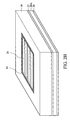
- FIGS. 1A to 1C are three-dimensional views illustrating a fabrication method for a pressure chamber of a piezoelectric ink jet print head according to the first embodiment of the present invention.
- FIGS. 2A to 2H illustrate a fabrication method for a pressure chamber and a vibrating layer of a piezoelectric ink jet print head according to the second embodiment of the present invention.
- FIGS. 3A to 3F are cross-sections illustrate a fabrication method for a pressure chamber and a vibrating layer of a piezoelectric ink jet print head according to the third embodiment of the present invention.
- the present invention provides a piezoelectric ink jet print head and a fabrication method for a pressure chamber thereof.
- a large-size opening is formed within a predetermined region of a silicon wafer through an enforceable etching method, and then filled with a photoresist layer.
- a plurality of small-size trenches spaced apart from each other is formed in the photoresist layer through a photolithography process or an enforceable etching method, thus each of the small-size trenches serves as a pressure chamber.
- the fabrication method for the pressure chamber can integrate another silicon wafer with adhesion, bonding, grinding and etching processes to complete a vibrating layer.
- the vibrating layer and the pressure chamber are applied to a bend-mode piezoelectric ink jet print head or a push-mode piezoelectric ink jet print head.
- FIGS. 1A to 1C are three-dimensional views illustrating a fabrication method for a pressure chamber of a piezoelectric ink jet print head according to the first embodiment of the present invention.
- a first silicon wafer 10 viewed as a frame, is provided with a large-size opening 12 within a predetermined region.
- the formation of the large-size opening 12 is selected from sand blasting, wet etching, dry etching or other enforceable etching methods. Also, depending on product specifications and process conditions, the quantity, size and profile of the large-size opening 12 can be appropriately modified.
- the large-size opening 12 has a square measurement of 10000 ⁇ m ⁇ 10000 ⁇ m. Then, in FIG.
- each of the small-size trenches 28 serves as a pressure chamber of a piezoelectric ink jet print head.
- the quantity, size and profile of the small-size trenches 28 can be appropriately modified.
- the small-size trench 28 has a rectangular measurement of 200 ⁇ m ⁇ 3000 ⁇ m.
- the second embodiment integrates the above-described fabrication method for the pressure chamber with wafer bonding, grinding, and etching to complete a vibrating layer.
- FIGS. 2A to 2H illustrate a fabrication method for a pressure chamber and a vibrating layer of a piezoelectric ink jet print head according to the second embodiment of the present invention.
- a first silicon wafer 10 is provided with a large-size opening 12 within a predetermined region.
- the formation of the large-size opening 12 in the second embodiment is substantially similar to that of the first embodiment, with the similar portion omitted herein.
- an SOI (silicon-on-insulator) technique is employed to bond the first silicon wafer 10 to another silicon wafer, resulting in a SOI substrate.
- a thermal oxidation process is used to grow a first silicon oxide layer 16 on the first silicon wafer 10 , and then a solution film 17 containing hydrogen bond (such as acetone or alcohol) is coated on the first silicon oxide layer 16 .
- a second silicon wafer 20 is provided with a second silicon oxide layer 18 grown thereon through a thermal oxidation process, and then a solution film 17 containing hydrogen bond (such as acetone or alcohol) is coated on the second silicon oxide layer 18 .
- a solution film 17 containing hydrogen bond such as acetone or alcohol
- a wafer bonding process is used to temporarily bond the second silicon oxide layer 18 downward to the first silicon oxide layer 16 through the solution film 17 , resulting in a silicon oxide adhesion layer 22 .
- a wafer alignment method and a wafer press method are used to tightly bond the second silicon wafer 20 downward to the first second silicon wafer 10 .
- a grinding process such as a chemical mechanical polishing (CMP) method, is used to polish the second silicon wafer 20 , thus the top portion 20 B is removed until the remaining portion 20 A reaches a thickness of 5 ⁇ 20 ⁇ m.
- the remaining silicon layer 20 A of the second silicon wafer 20 serves as a vibrating layer 20 A.
- a grinding process such as a chemical mechanical polishing (CMP) method, may be optionally used to polish the bottom of the first silicon wafer 10 until its thickness reaches a predetermined depth for a subsequent pressure chamber process.
- a piezoelectric material layer 26 is formed on the silicon layer 20 A.
- the large-size opening 12 of the first silicon wafer 10 is filled with a photoresist layer 14 .
- the silicon oxide adhesion layer 22 is used as a barrier layer, and a photolithography process or an enforceable etching method is performed on the photoresist layer 14 to form a plurality of small-size trenches 28 spaced apart from each other.
- each of the small-size trenches 28 serves as a pressure chamber.
- the formation of the pressure chamber employs the ordinary photolithography process including steps of soft baking, exposure, developing and hard baking to form the small-size trenches 28 in the photoresist layer 14 without performing a direct wet etching or a direct dry etching on the first silicon wafer 10 .
- the problems of bevel defects, low etching rate, and excessive process cost encountered in the conventional silicon etching process are avoided.
- the present invention integrates wafer bonding, grinding and etching to form the silicon layer 20 A as the vibrating layer from the top of the second silicon wafer 20 , and form the small-size trench 28 of the photoresist layer 14 as the pressure chamber from the bottom of the first silicon wafer 10 .
- the present invention can simplify the procedure, reduce process difficulties, and increase process reliability, resulting in high yield, low cost and great production.
- the fabrication method for a pressure chamber and a vibrating layer of a piezoelectric ink jet print head in the third embodiment is substantially similar to that of the second embodiment, with the similar portions omitted herein.
- the different portion is the wafer bonding method, in which an adhesion agent is used to replace the SOI technique so as to further simplify process steps and reduce process costs.
- FIGS. 3A to 3F are cross-sections illustrating a fabrication method for a pressure chamber and a vibrating layer of a piezoelectric ink jet print head according to the third embodiment of the present invention.
- a first silicon wafer 10 is provided with a large-size opening 12 within a predetermined region, and then an adhesion layer 24 is coated on the first silicon wafer 10 .
- a second silicon wafer 20 is provided with an adhesion layer 24 .
- the adhesion layer 24 is selected from resin, phosphosilicate glass (PSG), spin-on glass (SOG) or a dry film.
- the second silicon wafer 20 is placed downward to temporarily adhere to the first silicon wafer 10 through the adhesion layer 24 . Then, a wafer alignment method and a wafer press method are used to tightly bond the second silicon wafer 20 downward to the first second silicon wafer 10 .
- a grinding process such as a chemical mechanical polishing (CMP) method, is used to polish the second silicon wafer 20 until the remaining portion 20 A reaches a thickness of 5 ⁇ 20 ⁇ m.
- CMP chemical mechanical polishing
- a grinding process such as a chemical mechanical polishing (CMP) method, is optionally used to polish the bottom of the first silicon wafer 10 until its thickness reaches a predetermined depth for a subsequent pressure chamber process.
- a piezoelectric material layer 26 is formed on the silicon layer 20 A.
- the large-size opening 12 of the first silicon wafer 10 is filled with a photoresist layer 14 .
- the adhesion layer 24 is used as a barrier layer, and a photolithography process or an enforceable etching method is performed on the photoresist layer 14 to form a plurality of small-size trenches 28 spaced apart from each other.
- each of the small-size trenches 28 serves as a pressure chamber.
Landscapes
- Engineering & Computer Science (AREA)
- Manufacturing & Machinery (AREA)
- Particle Formation And Scattering Control In Inkjet Printers (AREA)
Abstract
A piezoelectric ink jet print head and a fabrication method for a pressure chamber thereof. A silicon substrate has at least one large-size opening. A photoresist layer is formed in the large-size opening of the silicon substrate and has a plurality of small-size trenches spaced apart from each other. Each of the small-size trenches serves as a pressure chamber. An adhesion layer is formed overlying the silicon substrate to cover the photoresist layer and the small-size trenches. A silicon layer is formed overlying the adhesion layer to serve as a vibrating layer.
Description
1. Field of the Invention
The invention relates to a pressure chamber of a piezoelectric ink jet print head and a fabrication method thereof, and more particularly to a fabrication method of forming a plurality of small-size trenches in a photoresist layer which fills a large-size opening of a silicon wafer.
2. Description of the Related Art
A piezoelectric ink jet print head employs a forced voltage to deform a piezoelectric ceramic body, and uses flexure displacement of the piezoelectric ceramic body to change the volume of a pressure chamber, thus the chamber expels an ink droplet. Since high-temperature gasification is omitted and the piezoelectric ceramic body has a quick response without restriction against thermal conductivity, the piezoelectric ink jet print head has the advantages of superior durability, high-speed print performance, and superior print quality. The piezoelectric ink jet print head has been commercialized into a bend mode and a push mode according to its deformation mechanism. The bend mode uses a face-shooter piezoelectric deformation. When a voltage is exerted, a piezoelectric ceramic body is deformed and impeded by a vibrating plate, thus being laterally and extruding the ink in a pressure chamber. As a voltage difference arises between the internal space and the external circumstance, the ink adjacent to a nozzle orifice is accelerated and expelled as an ink droplet. Comparably, the push mode uses an edge-shooter piezoelectric deformation. When an opposite potential of the applied voltage between the two electrodes is continuously increased, a ceramic sidewall of an ink chamber bends outward to introduce ink. When the applied voltage is rapidly changed, a piezoelectric ceramic plate is deformed to cause a greater bending motion, thus the ink in the pressure chamber is extruded by a right-hand thrust and expelled from a nozzle orifice to form an ink droplet.
Conventionally, the vibrating plate and the pressure chamber are formed by a laminated ceramic co-fired method which includes steps of synthesizing raw powers (such as PZT, ZrO2, Pbo, TiO2 and other additives), mixing, drying, calcining, smashing, granulation, squeezing, shaping, sintering and polarization. The complicated and difficult procedure in the laminated ceramic co-fired method, however, has disadvantages of low yield and high cost and is unfavorable to mass production. Accordingly, a modified etching process for forming the pressure chamber and increasing process reliability thereof is called for.
Currently, in semiconductor etching processing, many approaches to a deep-hole etching technique have been developed and successfully applied to micro electromechanical structures. The deep-hole etching technique, such as a wet etching method through a chemical reaction or a dry etching process through a physical reaction, however, has the drawbacks of directional etching result, low etching rate and excessive process costs. Conventionally, a direct Si-wafer etching process cannot control the profile, depth, and uniformity of the pressure chambers, which causes the piezoelectric ink jet print head to fail in a high resolution performance.
Accordingly, an object of the present invention is to provide a fabrication method with wafer bonding, grinding, oxidation, photoresist filling, photolithography and etching for a pressure chamber of a piezoelectric ink jet print head to solve the problems caused by the conventional method.
According to the object of the invention, a fabrication method for a piezoelectric ink jet print head comprises the following steps. A silicon substrate is provided with at least one large-size opening. Then, the large-size opening of the silicon substrate is filled with a photoresist layer. Next, photolithography or etching is performed on the photoresist layer to form a plurality of small-size trenches spaced apart from each other, thus the small-size trench serves as a pressure chamber.
Another object of the present invention is to provide a fabrication method with wafer bonding, grinding, oxidation, photoresist filling, photolithography, and etching for a pressure chamber and a vibrating layer of a piezoelectric ink jet print head to solve the problems caused by the conventional method.
According to the object of the invention, a fabrication method for a piezoelectric ink jet print head includes the following steps. A first silicon wafer is provided with at least one large-size opening. Then, a second silicon wafer is provided. Next, an oxidation process is performed to form a first oxide layer overlying the first silicon wafer and a second oxide layer overlying the second silicon wafer. Next, a wafer bonding process is performed to bond the second silicon wafer to the first silicon wafer, in which the second oxide layer adheres to the first oxide layer to become an adhesion layer. Next, a grinding process is performed on the outer surface of the second silicon wafer, in which the remaining portion of the second silicon wafer serves as a silicon layer. Next, a piezoelectric material layer is formed overlying the silicon layer. Next, the large-size opening of the silicon substrate is filled with a photoresist layer. Finally, photolithography or etching is performed on the photoresist layer and the adhesion layer is used as a barrier layer, resulting in a plurality of small-size trenches spaced apart from each other.
The present invention will become more fully understood from the detailed description given hereinbelow and the accompanying drawings, given by way of illustration only and thus not intended to be limitative of the present invention.
The present invention provides a piezoelectric ink jet print head and a fabrication method for a pressure chamber thereof. First, a large-size opening is formed within a predetermined region of a silicon wafer through an enforceable etching method, and then filled with a photoresist layer. Next, a plurality of small-size trenches spaced apart from each other is formed in the photoresist layer through a photolithography process or an enforceable etching method, thus each of the small-size trenches serves as a pressure chamber. Also, the fabrication method for the pressure chamber can integrate another silicon wafer with adhesion, bonding, grinding and etching processes to complete a vibrating layer. The vibrating layer and the pressure chamber are applied to a bend-mode piezoelectric ink jet print head or a push-mode piezoelectric ink jet print head.
First Embodiment
Second Embodiment
The second embodiment integrates the above-described fabrication method for the pressure chamber with wafer bonding, grinding, and etching to complete a vibrating layer.
In a three-dimensional view of FIG. 2A , a first silicon wafer 10 is provided with a large-size opening 12 within a predetermined region. The formation of the large-size opening 12 in the second embodiment is substantially similar to that of the first embodiment, with the similar portion omitted herein.
Then, an SOI (silicon-on-insulator) technique is employed to bond the first silicon wafer 10 to another silicon wafer, resulting in a SOI substrate. In a cross-section of FIG. 2B , a thermal oxidation process is used to grow a first silicon oxide layer 16 on the first silicon wafer 10, and then a solution film 17 containing hydrogen bond (such as acetone or alcohol) is coated on the first silicon oxide layer 16. In the meantime, a second silicon wafer 20 is provided with a second silicon oxide layer 18 grown thereon through a thermal oxidation process, and then a solution film 17 containing hydrogen bond (such as acetone or alcohol) is coated on the second silicon oxide layer 18. Next, in the cross-section of FIG. 2C , a wafer bonding process is used to temporarily bond the second silicon oxide layer 18 downward to the first silicon oxide layer 16 through the solution film 17, resulting in a silicon oxide adhesion layer 22. Then, a wafer alignment method and a wafer press method are used to tightly bond the second silicon wafer 20 downward to the first second silicon wafer 10. Next, in a cross-section of FIG. 2D , a grinding process, such as a chemical mechanical polishing (CMP) method, is used to polish the second silicon wafer 20, thus the top portion 20B is removed until the remaining portion 20A reaches a thickness of 5˜20 μm. Thus, the remaining silicon layer 20A of the second silicon wafer 20 serves as a vibrating layer 20A. A grinding process, such as a chemical mechanical polishing (CMP) method, may be optionally used to polish the bottom of the first silicon wafer 10 until its thickness reaches a predetermined depth for a subsequent pressure chamber process.
Next, in a cross-section of FIG. 2E , a piezoelectric material layer 26 is formed on the silicon layer 20A. Then, in a cross-section of FIG. 2F , the large-size opening 12 of the first silicon wafer 10 is filled with a photoresist layer 14. Finally, in a cross-section shown in FIG. 2G and a three-dimensional view of FIG. 2H , the silicon oxide adhesion layer 22 is used as a barrier layer, and a photolithography process or an enforceable etching method is performed on the photoresist layer 14 to form a plurality of small-size trenches 28 spaced apart from each other. Thus, each of the small-size trenches 28 serves as a pressure chamber.
Subsequent processes for an ink slot, nozzle orifices and a nozzle plate will be performed under the pressure chamber, which are omitted herein.
The formation of the pressure chamber employs the ordinary photolithography process including steps of soft baking, exposure, developing and hard baking to form the small-size trenches 28 in the photoresist layer 14 without performing a direct wet etching or a direct dry etching on the first silicon wafer 10. Thus, the problems of bevel defects, low etching rate, and excessive process cost encountered in the conventional silicon etching process are avoided. Also, the present invention integrates wafer bonding, grinding and etching to form the silicon layer 20A as the vibrating layer from the top of the second silicon wafer 20, and form the small-size trench 28 of the photoresist layer 14 as the pressure chamber from the bottom of the first silicon wafer 10. Thus, the present invention can simplify the procedure, reduce process difficulties, and increase process reliability, resulting in high yield, low cost and great production.
Third Embodiment
The fabrication method for a pressure chamber and a vibrating layer of a piezoelectric ink jet print head in the third embodiment is substantially similar to that of the second embodiment, with the similar portions omitted herein. The different portion is the wafer bonding method, in which an adhesion agent is used to replace the SOI technique so as to further simplify process steps and reduce process costs.
In FIG. 3A , a first silicon wafer 10 is provided with a large-size opening 12 within a predetermined region, and then an adhesion layer 24 is coated on the first silicon wafer 10. A second silicon wafer 20 is provided with an adhesion layer 24. Preferably, the adhesion layer 24 is selected from resin, phosphosilicate glass (PSG), spin-on glass (SOG) or a dry film.
Next, in FIG. 3B , the second silicon wafer 20 is placed downward to temporarily adhere to the first silicon wafer 10 through the adhesion layer 24. Then, a wafer alignment method and a wafer press method are used to tightly bond the second silicon wafer 20 downward to the first second silicon wafer 10.
Next, in FIG. 3C , a grinding process, such as a chemical mechanical polishing (CMP) method, is used to polish the second silicon wafer 20 until the remaining portion 20A reaches a thickness of 5˜20 μm. Thus, the remaining silicon layer 20A serves as a vibrating layer 20A. A grinding process, such as a chemical mechanical polishing (CMP) method, is optionally used to polish the bottom of the first silicon wafer 10 until its thickness reaches a predetermined depth for a subsequent pressure chamber process.
Next, in FIG. 3D , a piezoelectric material layer 26 is formed on the silicon layer 20A. Then, in FIG. 3E , the large-size opening 12 of the first silicon wafer 10 is filled with a photoresist layer 14. Finally, in FIG. 3F , the adhesion layer 24 is used as a barrier layer, and a photolithography process or an enforceable etching method is performed on the photoresist layer 14 to form a plurality of small-size trenches 28 spaced apart from each other. Thus, each of the small-size trenches 28 serves as a pressure chamber.
Subsequent processes for an ink slot, nozzle orifices and a nozzle plate will be performed under the pressure chamber, which are omitted herein.
While the invention has been described by way of example and in terms of the preferred embodiments, it is to be understood that the invention is not limited to the disclosed embodiments. To the contrary, it is intended to cover various modifications and similar arrangements (as would be apparent to those skilled in the art). Therefore, the scope of the appended claims should be accorded the broadest interpretation so as to encompass all such modifications and similar arrangements.
Claims (2)
1. A fabrication method for a piezoelectric ink jet head, comprising steps of:
providing a silicon substrate comprising at least one large-size opening;
filling the at least one large-size opening of the silicon substrate with a photoresist layer; and
performing photolithography or etching on the photoresist layer to form a plurality of isolated small-size trenches spaced apart from each other, in which each isolated small-size trench serves as a pressure chamber.
2. The fabrication method for a piezoelectric ink jet print head as claimed in claim 1 , wherein the at least one large-size opening is formed by wet etching or dry etching.
Applications Claiming Priority (2)
| Application Number | Priority Date | Filing Date | Title |
|---|---|---|---|
| TW091120855A TW553836B (en) | 2002-09-12 | 2002-09-12 | Piezoelectric inkjet head and method for forming pressure chamber thereof |
| TW91120855 | 2002-09-12 |
Publications (2)
| Publication Number | Publication Date |
|---|---|
| US20040051760A1 US20040051760A1 (en) | 2004-03-18 |
| US6981300B2 true US6981300B2 (en) | 2006-01-03 |
Family
ID=31974940
Family Applications (1)
| Application Number | Title | Priority Date | Filing Date |
|---|---|---|---|
| US10/653,621 Expired - Fee Related US6981300B2 (en) | 2002-09-12 | 2003-09-02 | Piezoelectric ink jet print head and fabrication method for a pressure chamber thereof |
Country Status (2)
| Country | Link |
|---|---|
| US (1) | US6981300B2 (en) |
| TW (1) | TW553836B (en) |
Cited By (1)
| Publication number | Priority date | Publication date | Assignee | Title |
|---|---|---|---|---|
| US20090176322A1 (en) * | 2008-01-04 | 2009-07-09 | Joyner Ii Burton L | Method for fabricating an ink jetting device |
Families Citing this family (2)
| Publication number | Priority date | Publication date | Assignee | Title |
|---|---|---|---|---|
| US20100252103A1 (en) * | 2009-04-03 | 2010-10-07 | Chiu-Lin Yao | Photoelectronic element having a transparent adhesion structure and the manufacturing method thereof |
| CN103258931B (en) * | 2009-04-28 | 2016-05-04 | 晶元光电股份有限公司 | Photoelectric element with transparent bonded structure and manufacturing method thereof |
Citations (4)
| Publication number | Priority date | Publication date | Assignee | Title |
|---|---|---|---|---|
| US5581861A (en) * | 1993-02-01 | 1996-12-10 | At&T Global Information Solutions Company | Method for making a solid-state ink jet print head |
| US6096656A (en) * | 1999-06-24 | 2000-08-01 | Sandia Corporation | Formation of microchannels from low-temperature plasma-deposited silicon oxynitride |
| US6334670B1 (en) * | 1998-12-03 | 2002-01-01 | Canon Kabushiki Kaisha | Method for manufacturing liquid jet head, liquid jet head, head cartridge, and liquid jet recording apparatus |
| US6701593B2 (en) * | 2001-01-08 | 2004-03-09 | Nanodynamics, Inc. | Process for producing inkjet printhead |
-
2002
- 2002-09-12 TW TW091120855A patent/TW553836B/en not_active IP Right Cessation
-
2003
- 2003-09-02 US US10/653,621 patent/US6981300B2/en not_active Expired - Fee Related
Patent Citations (4)
| Publication number | Priority date | Publication date | Assignee | Title |
|---|---|---|---|---|
| US5581861A (en) * | 1993-02-01 | 1996-12-10 | At&T Global Information Solutions Company | Method for making a solid-state ink jet print head |
| US6334670B1 (en) * | 1998-12-03 | 2002-01-01 | Canon Kabushiki Kaisha | Method for manufacturing liquid jet head, liquid jet head, head cartridge, and liquid jet recording apparatus |
| US6096656A (en) * | 1999-06-24 | 2000-08-01 | Sandia Corporation | Formation of microchannels from low-temperature plasma-deposited silicon oxynitride |
| US6701593B2 (en) * | 2001-01-08 | 2004-03-09 | Nanodynamics, Inc. | Process for producing inkjet printhead |
Cited By (1)
| Publication number | Priority date | Publication date | Assignee | Title |
|---|---|---|---|---|
| US20090176322A1 (en) * | 2008-01-04 | 2009-07-09 | Joyner Ii Burton L | Method for fabricating an ink jetting device |
Also Published As
| Publication number | Publication date |
|---|---|
| US20040051760A1 (en) | 2004-03-18 |
| TW553836B (en) | 2003-09-21 |
Similar Documents
| Publication | Publication Date | Title |
|---|---|---|
| US7121650B2 (en) | Piezoelectric ink-jet printhead | |
| US6794723B2 (en) | Matrix type piezoelectric/electrostrictive device and manufacturing method thereof | |
| JP2013538446A (en) | Formation of devices with curved piezoelectric films | |
| JP2018124275A (en) | Semiconductor sensor device and manufacturing method thereof | |
| US8828750B2 (en) | Highly integrated wafer bonded MEMS devices with release-free membrane manufacture for high density print heads | |
| US6981300B2 (en) | Piezoelectric ink jet print head and fabrication method for a pressure chamber thereof | |
| KR100682917B1 (en) | Piezoelectric inkjet printheads and manufacturing method thereof | |
| US20040056930A1 (en) | Piezoelectric ink jet print head and fabrication method for a vibrating layer thereof | |
| US7185972B2 (en) | Method of manufacturing printer head, and method of manufacturing electrostatic actuator | |
| US20040104976A1 (en) | Pressure chamber of a piezoelectric ink jet print head and fabrication method thereof | |
| US6443562B1 (en) | Integrally formed driving module for an ink jet apparatus and method for manufacturing it | |
| US6693045B2 (en) | High density wafer production method | |
| CN1490160A (en) | Piezoelectric ink jet head and pressure cavity forming method thereof | |
| TW504769B (en) | Forming method of piezoelectric ink jet chip | |
| KR100474836B1 (en) | Manufacturing method for monolithic fluid jet printer head | |
| JPH1134319A (en) | Recording head | |
| JP2003011359A (en) | Ink jet head and method of manufacturing the same | |
| CN112808330A (en) | Method for manufacturing micro-fluid actuator | |
| JP2002029053A (en) | ELECTROSTATIC ACTUATOR, METHOD OF MANUFACTURING THE ELECTROSTATIC ACTUATOR, INK JET PRINT HEAD HAVING THE ELECTROSTATIC ACTUATOR, AND INK JET PRINTING APPARATUS EQUIPPED WITH THE INK JET PRINT HEAD | |
| JP2007038452A (en) | Electrostatic actuator and manufacturing method thereof, droplet discharge head and manufacturing method thereof, device, and droplet discharge apparatus | |
| JP2001347673A (en) | Inkjet head structure, inkjet head manufacturing method, and image forming apparatus | |
| JP2008044302A (en) | Electrode glass substrate manufacturing method, electrode glass substrate, electrostatic actuator manufacturing method, electrostatic actuator, and droplet discharge head | |
| KR20000031873A (en) | Head of ink jet printer and method of production the same | |
| JP2002264089A (en) | Microactuator, method of manufacturing the same, inkjet head and method of manufacturing the same | |
| JP2007111950A (en) | Electrostatic actuator manufacturing method, droplet discharge head manufacturing method, droplet discharge apparatus manufacturing method, and device manufacturing method |
Legal Events
| Date | Code | Title | Description |
|---|---|---|---|
| AS | Assignment |
Owner name: NANODYNAMICS INC., TAIWAN Free format text: ASSIGNMENT OF ASSIGNORS INTEREST;ASSIGNORS:TSAI, CHIH-CHANG;YANG, MING-HSUN;REEL/FRAME:014461/0037;SIGNING DATES FROM 20030814 TO 20030815 |
|
| REMI | Maintenance fee reminder mailed | ||
| LAPS | Lapse for failure to pay maintenance fees | ||
| STCH | Information on status: patent discontinuation |
Free format text: PATENT EXPIRED DUE TO NONPAYMENT OF MAINTENANCE FEES UNDER 37 CFR 1.362 |
|
| FP | Lapsed due to failure to pay maintenance fee |
Effective date: 20100103 |