US6952354B1 - Single stage PFC power converter - Google Patents
Single stage PFC power converter Download PDFInfo
- Publication number
- US6952354B1 US6952354B1 US10/859,811 US85981104A US6952354B1 US 6952354 B1 US6952354 B1 US 6952354B1 US 85981104 A US85981104 A US 85981104A US 6952354 B1 US6952354 B1 US 6952354B1
- Authority
- US
- United States
- Prior art keywords
- side switch
- power converter
- bulk capacitor
- coupled
- terminal
- Prior art date
- Legal status (The legal status is an assumption and is not a legal conclusion. Google has not performed a legal analysis and makes no representation as to the accuracy of the status listed.)
- Expired - Lifetime
Links
- 239000003990 capacitor Substances 0.000 claims abstract description 40
- 238000004804 winding Methods 0.000 claims abstract description 27
- 229920006395 saturated elastomer Polymers 0.000 claims description 2
- 238000010586 diagram Methods 0.000 description 6
- 239000008186 active pharmaceutical agent Substances 0.000 description 2
- 230000001105 regulatory effect Effects 0.000 description 2
- 230000004907 flux Effects 0.000 description 1
- 230000017525 heat dissipation Effects 0.000 description 1
- 238000000034 method Methods 0.000 description 1
- 238000012986 modification Methods 0.000 description 1
- 230000004048 modification Effects 0.000 description 1
Images


Classifications
-
- H—ELECTRICITY
- H02—GENERATION; CONVERSION OR DISTRIBUTION OF ELECTRIC POWER
- H02M—APPARATUS FOR CONVERSION BETWEEN AC AND AC, BETWEEN AC AND DC, OR BETWEEN DC AND DC, AND FOR USE WITH MAINS OR SIMILAR POWER SUPPLY SYSTEMS; CONVERSION OF DC OR AC INPUT POWER INTO SURGE OUTPUT POWER; CONTROL OR REGULATION THEREOF
- H02M1/00—Details of apparatus for conversion
- H02M1/42—Circuits or arrangements for compensating for or adjusting power factor in converters or inverters
- H02M1/4208—Arrangements for improving power factor of AC input
- H02M1/4258—Arrangements for improving power factor of AC input using a single converter stage both for correction of AC input power factor and generation of a regulated and galvanically isolated DC output voltage
-
- H—ELECTRICITY
- H02—GENERATION; CONVERSION OR DISTRIBUTION OF ELECTRIC POWER
- H02M—APPARATUS FOR CONVERSION BETWEEN AC AND AC, BETWEEN AC AND DC, OR BETWEEN DC AND DC, AND FOR USE WITH MAINS OR SIMILAR POWER SUPPLY SYSTEMS; CONVERSION OF DC OR AC INPUT POWER INTO SURGE OUTPUT POWER; CONTROL OR REGULATION THEREOF
- H02M3/00—Conversion of dc power input into dc power output
- H02M3/22—Conversion of dc power input into dc power output with intermediate conversion into ac
- H02M3/24—Conversion of dc power input into dc power output with intermediate conversion into ac by static converters
- H02M3/28—Conversion of dc power input into dc power output with intermediate conversion into ac by static converters using discharge tubes with control electrode or semiconductor devices with control electrode to produce the intermediate ac
- H02M3/325—Conversion of dc power input into dc power output with intermediate conversion into ac by static converters using discharge tubes with control electrode or semiconductor devices with control electrode to produce the intermediate ac using devices of a triode or a transistor type requiring continuous application of a control signal
- H02M3/335—Conversion of dc power input into dc power output with intermediate conversion into ac by static converters using discharge tubes with control electrode or semiconductor devices with control electrode to produce the intermediate ac using devices of a triode or a transistor type requiring continuous application of a control signal using semiconductor devices only
- H02M3/3353—Conversion of dc power input into dc power output with intermediate conversion into ac by static converters using discharge tubes with control electrode or semiconductor devices with control electrode to produce the intermediate ac using devices of a triode or a transistor type requiring continuous application of a control signal using semiconductor devices only having at least two simultaneously operating switches on the input side, e.g. "double forward" or "double (switched) flyback" converter
-
- Y—GENERAL TAGGING OF NEW TECHNOLOGICAL DEVELOPMENTS; GENERAL TAGGING OF CROSS-SECTIONAL TECHNOLOGIES SPANNING OVER SEVERAL SECTIONS OF THE IPC; TECHNICAL SUBJECTS COVERED BY FORMER USPC CROSS-REFERENCE ART COLLECTIONS [XRACs] AND DIGESTS
- Y02—TECHNOLOGIES OR APPLICATIONS FOR MITIGATION OR ADAPTATION AGAINST CLIMATE CHANGE
- Y02B—CLIMATE CHANGE MITIGATION TECHNOLOGIES RELATED TO BUILDINGS, e.g. HOUSING, HOUSE APPLIANCES OR RELATED END-USER APPLICATIONS
- Y02B70/00—Technologies for an efficient end-user side electric power management and consumption
- Y02B70/10—Technologies improving the efficiency by using switched-mode power supplies [SMPS], i.e. efficient power electronics conversion e.g. power factor correction or reduction of losses in power supplies or efficient standby modes
-
- Y—GENERAL TAGGING OF NEW TECHNOLOGICAL DEVELOPMENTS; GENERAL TAGGING OF CROSS-SECTIONAL TECHNOLOGIES SPANNING OVER SEVERAL SECTIONS OF THE IPC; TECHNICAL SUBJECTS COVERED BY FORMER USPC CROSS-REFERENCE ART COLLECTIONS [XRACs] AND DIGESTS
- Y02—TECHNOLOGIES OR APPLICATIONS FOR MITIGATION OR ADAPTATION AGAINST CLIMATE CHANGE
- Y02P—CLIMATE CHANGE MITIGATION TECHNOLOGIES IN THE PRODUCTION OR PROCESSING OF GOODS
- Y02P80/00—Climate change mitigation technologies for sector-wide applications
- Y02P80/10—Efficient use of energy, e.g. using compressed air or pressurized fluid as energy carrier
Definitions
- the present invention relates to a power converter, and more particularly, to a power factor correction (PFC) power converter in single stage.
- PFC power factor correction
- Power converters have widely served to convert an unregulated power source to a regulated voltage or current.
- a PFC (Power Factor Correction) technique is applied to make an input current follow the waveform of an input voltage. Adding a PFC stage to the front end of a power converter substantially avoids unnecessary power losses and heat dissipation in a power contribution system.
- a power converter having two stages is illustrated.
- a first stage is a PFC stage, which includes an inductor 13 , a rectifier 16 and a transistor 10 .
- the transistor 10 is driven by a control signal PFC from the PFC stage.
- a second stage includes a transistor 15 controlled by a control signal PWM, a transformer 50 and a secondary circuitry, thus output voltage is regulated and output ripple noise is reduced.
- the PFC stage configuration increases the cost and device counts of the power converter, and hence efficiency of the power converter is reduced. Therefore, the development trend of power converters is to build a single stage power converter with PFC function.
- the present invention provides a single stage PFC power converter to reduce the cost and the size, i.e. device counts, and to improve efficiency of the power converter.
- the present invention also reduces output ripple noise.
- the present invention can further provide a power converter operating in lower stress to obtain higher reliability.
- the present invention provides a single stage power factor correction (PFC) power converter that performs a PFC function to a half-bridge flyback power converter.
- the single stage PFC power converter includes a transformer having a primary winding coupled to a high side switch and a low-side switch in series, and a secondary winding coupled to a secondary circuit.
- the high-side and low-side switches periodically couple an input voltage to the primary winding of the transformer. Once the high-side switch and the low-side switch are switched off, an energy stored in the transformer will be transmitted to the secondary circuit. Meanwhile the energy will be charged to a bulk capacitor through a first flyback diode and a second flyback diode.
- a forward diode and a forward inductor serve to forward the energy of the bulk capacitor to the flowing path of the input voltage for performing PFC function.
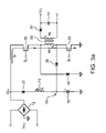
- FIG. 1 is a schematic diagram illustrating a power converter according to prior art.
- FIG. 2 is a schematic diagram illustrating a single stage PFC power converter according to one embodiment of the present invention.
- FIG. 3 a is a schematic diagram of the single stage PFC power converter illustrating a high-side switch and a low-side switch being switched on according to one embodiment of the present invention.
- FIG. 3 b is a schematic diagram of the single stage PFC power converter illustrating the high-side switch and the low-side switch being switched off according to one embodiment of the present invention.
- FIG. 4 is a schematic diagram of the single stage PFC power converter illustrating the status when an input voltage is lower than a voltage of a bulk capacitor according to one embodiment of the present invention.
- FIG. 5 is a schematic waveform diagram of an input current and the input voltage of the single stage PFC power converter according to one embodiment of the present invention.
- the single stage PFC power converter includes a transformer 55 having a primary winding N P , a secondary winding N S , a secondary circuit, a high-side switch 30 , a low-side switch 35 , flyback diodes 25 and 26 , a forward diode 20 , a bulk capacitor 60 , a forward inductor 70 , and a bridge rectifier 12 .
- the bridge rectifier 12 rectifies an AC line voltage V AC to an input voltage V IN .
- a first terminal of the high-side switch 30 is supplied with the input voltage V IN .
- a second terminal of the high-side switch 30 is connected to a second terminal of the primary winding N P .
- a first terminal of the primary winding N P is coupled to a first terminal of the low-side switch 35 .
- a second terminal of the low-side switch 35 is coupled to a ground reference level.
- the secondary winding N S of the transformer 55 is coupled to the secondary circuit.
- the secondary circuit includes an output rectifier 51 having an anode coupled to a first terminal of the secondary winding N S and a cathode coupled to an output capacitor 52 .
- the output capacitor 52 is coupled to the output terminals of the power converter in parallel.
- the first terminal of the primary winding N P and the first terminal of the secondary winding N S possess same polarity.
- the high-side switch 30 and the low-side switch 35 periodically couple the input voltage V IN to the primary winding N P of the transformer 55 .
- a magnetized energy ⁇ P will be stored in the transformer 55 .
- the transformer 55 magnetized by a primary current I P when the high-side switch 30 and the low-side switch 35 are switched on according to one embodiment of the present invention is illustrated. Meanwhile an energy ⁇ I , is stored in the leakage inductor L I of the transformer 55 .
- the leakage inductor L I indicates a magnetic flux that cannot be transferred to the secondary side of the transformer 55 .
- ⁇ I 1 2 ⁇ L I ⁇ P P 2 ( 2 )
- An anode of the flyback diode 25 is coupled to the ground reference level and a cathode of the flyback diode 25 is coupled to the second terminal of the primary winding N P .
- An anode of the flyback diode 26 is coupled to the first terminal of the primary winding N P .
- a cathode of the flyback diode 26 is coupled to a positive terminal of the bulk capacitor 60 .
- a negative terminal of the bulk capacitor 60 is coupled to the ground reference level.
- the forward diode 20 is coupled to the forward inductor 70 in series.
- a cathode of the forward diode 20 is coupled to the input voltage V IN
- an anode of the forward diode 20 is coupled to a terminal of the forward inductor 70 .
- the other terminal of the forward inductor 70 is coupled to the positive terminal of the bulk capacitor 60 .
- the magnetized energy ⁇ P stored in the transformer 55 is transmitted to the secondary circuit through the secondary winding N S as the high-side switch 30 and the low-side switch 35 are both switched off according to one embodiment of the present invention.
- the bulk capacitor 60 is charged by the energy ⁇ P and ⁇ I through the flyback diodes 25 and 26 .
- the forward diode 20 is reverse-biased. Therefore, a main switching current is only provided by the input voltage V IN as the high-side switch 30 and the low-side switch 35 are both switched on.
- the forward diode 20 and the forward inductor 70 serve to forward the energy of the bulk capacitor 60 to the flowing path of the input voltage V IN .
- the energy stored in the bulk capacitor 60 will start to power the secondary circuit, which reduces the output ripple noise.
- a turn-ratio of the transformer 55 and an output voltage V O determine the voltage V B across the bulk capacitor 60 .
- the current flowing through the high-side switch 30 and the low-side switch 35 when the input voltage V IN is lower than the voltage V B of the bulk capacitor 60 according to one embodiment of the present invention is illustrated.
- the forward inductor 70 provides a propagation delay for an auxiliary current that is supplied by the bulk capacitor 60 .
- the input voltage V IN provides the main switching current before the forward inductor 70 is saturated. Therefore, the input current waveform is improved with superior PFC performance.
- FIG. 5 the waveforms of the input current I IN and the input voltage V IN are depicted.
- a capacitor 42 and a snubber resistor 41 serving to store and consume the energy of the leakage inductor of the transformer 50 are illustrated.
- the energy of the leakage inductor must be completely dissipated; otherwise the drain voltage of the transistor 15 will continuously increases until the power consumption in the snubber resistor 41 fully dissipates the energy of the leakage inductor.
- an NTC (negative temperature coefficient) thermistor 11 shown in the FIG. 1 serves to avoid a current surge of the power converter. A current surge will be generated when the power converter is turned on due to the charge of the capacitor 18 . The current surge reduces the reliability of the power converter. In addition, the NTC thermistor increases the power consumption and operating temperature.
- the energy of the leakage inductor is stored into the buck capacitor 60 .
- No snubber component is needed for dissipating the energy stored in the leakage inductor. This energy is further recycled for supplying the secondary circuit. Therefore, the power efficiency of the power converter is improved.
- the voltage V B of the bulk capacitor 60 clamps the operating voltage of the low-side switch 35 .
- the input voltage V IN clamps the operating voltage of the high-side switch 30 .
- the voltage stress of the high-side switch 30 and the low-side switches 35 of the present invention can be reduced.
- the high-side switch 30 blocks the path from the input voltage V IN to the bulk capacitor 60 .
- the bulk capacitor 60 can only be gradually charged by the magnetized energy ⁇ P of the transformer 55 and the energy ⁇ I of the leakage inductor, which eliminates the need of NTC thermistor and further improves the efficiency and the reliability of the power converter.
Landscapes
- Engineering & Computer Science (AREA)
- Power Engineering (AREA)
- Dc-Dc Converters (AREA)
- Rectifiers (AREA)
Abstract
Description
where VR41 is the voltage across the
V DS =V IN +V R41 (5)
From equation (5), it is known that the operating stress of the
Claims (8)
Priority Applications (1)
| Application Number | Priority Date | Filing Date | Title |
|---|---|---|---|
| US10/859,811 US6952354B1 (en) | 2004-06-03 | 2004-06-03 | Single stage PFC power converter |
Applications Claiming Priority (1)
| Application Number | Priority Date | Filing Date | Title |
|---|---|---|---|
| US10/859,811 US6952354B1 (en) | 2004-06-03 | 2004-06-03 | Single stage PFC power converter |
Publications (1)
| Publication Number | Publication Date |
|---|---|
| US6952354B1 true US6952354B1 (en) | 2005-10-04 |
Family
ID=35005161
Family Applications (1)
| Application Number | Title | Priority Date | Filing Date |
|---|---|---|---|
| US10/859,811 Expired - Lifetime US6952354B1 (en) | 2004-06-03 | 2004-06-03 | Single stage PFC power converter |
Country Status (1)
| Country | Link |
|---|---|
| US (1) | US6952354B1 (en) |
Cited By (22)
| Publication number | Priority date | Publication date | Assignee | Title |
|---|---|---|---|---|
| US20060007711A1 (en) * | 2004-07-12 | 2006-01-12 | Ta-Yung Yang | Half-bridge flyback power converter |
| US20070297197A1 (en) * | 2006-06-26 | 2007-12-27 | System General Corp. | High efficiency switching power converter |
| US20090059455A1 (en) * | 2007-08-31 | 2009-03-05 | Texas Instruments Incorporated | Method and apparatus for power interruption protection |
| US20100002469A1 (en) * | 2008-07-01 | 2010-01-07 | George Young | Control circuit for a buck power factor correction stage |
| US20100067270A1 (en) * | 2008-09-15 | 2010-03-18 | Power Integrations, Inc. | Method and apparatus to reduce line current harmonics from a power supply |
| US20100118573A1 (en) * | 2008-11-07 | 2010-05-13 | Power Integrations, Inc. | Method and apparatus to increase efficiency in a power factor correction circuit |
| US20100118571A1 (en) * | 2008-11-07 | 2010-05-13 | Power Integrations, Inc. | Method and apparatus to control a power factor correction circuit |
| EP2187515A1 (en) * | 2008-11-12 | 2010-05-19 | Magneti Marelli S.p.A. | DC-DC forward converter apparatus and corresponding conversion method |
| US20100165669A1 (en) * | 2008-12-31 | 2010-07-01 | Macroblock, Inc. | Single-stage isolated high power factor ac/dc converter with leakage inductor energy recovery function |
| US20100202163A1 (en) * | 2009-02-10 | 2010-08-12 | System General Corporation | Flyback power converters |
| US20100315058A1 (en) * | 2009-06-16 | 2010-12-16 | Chi-Shun Liao | Power supply apparatus with inrush current prevention circuit |
| CN102223072A (en) * | 2010-06-25 | 2011-10-19 | 崇贸科技股份有限公司 | Double-switch flyback type power converter with wide input voltage range |
| WO2013012529A1 (en) * | 2011-07-15 | 2013-01-24 | Osram Sylvania Inc. | Resonate driver for solid state light sources |
| US20130100710A1 (en) * | 2011-10-21 | 2013-04-25 | Power Integrations, Inc. | Active surge protection in a power supply |
| WO2013074433A2 (en) | 2011-11-14 | 2013-05-23 | Cognipower, Llc | Switched-mode compound power converter with main and supplemental regulators |
| US20140028096A1 (en) * | 2012-07-24 | 2014-01-30 | Hon Hai Precision Industry Co., Ltd. | Rectifier circuit and electronic device using same |
| US20150222177A1 (en) * | 2014-02-03 | 2015-08-06 | Fuxiang LIN | High efficient single stage half bridge power factor correction converter |
| CN104167914B (en) * | 2014-09-10 | 2016-11-30 | 西南石油大学 | High power factor converter |
| CN106787860A (en) * | 2016-12-30 | 2017-05-31 | 杭州禾迈电力电子技术有限公司 | A kind of single-stage isolated type Three-phase PFC |
| US10461654B2 (en) | 2017-05-04 | 2019-10-29 | Dell Products, Lp | Power supply light load efficiency control circuit |
| EP3591825A1 (en) * | 2018-07-03 | 2020-01-08 | ABB Schweiz AG | Hybrid flyback converter |
| CN112803752A (en) * | 2021-03-19 | 2021-05-14 | 深圳原能电器有限公司 | Valley-filling and stroboflash-free PFC converter and control method |
Citations (7)
| Publication number | Priority date | Publication date | Assignee | Title |
|---|---|---|---|---|
| DE3133578A1 (en) * | 1981-08-25 | 1983-03-17 | Siemens AG, 1000 Berlin und 8000 München | Single-ended forward converter |
| US6031748A (en) * | 1998-02-06 | 2000-02-29 | Lg Electronics Inc. | Power saving circuit of power factor adjusting type |
| US6507500B2 (en) * | 2001-01-20 | 2003-01-14 | Skynet Electronic Co., Ltd. | Ring-free zero-voltage switching technique for use in switching power converters |
| US6538906B1 (en) * | 2002-02-11 | 2003-03-25 | Delta Electronics, Inc. | Energy storage circuit for DC-DC converter |
| US6717827B2 (en) * | 2001-12-21 | 2004-04-06 | Fuji Electric Co., Ltd | Switching power supply |
| US6862197B2 (en) * | 2001-01-26 | 2005-03-01 | Telefonaktiebolaget Lm Ericsson (Publ) | Arrangement for demagnetizing a transformer |
| US6862194B2 (en) * | 2003-06-18 | 2005-03-01 | System General Corp. | Flyback power converter having a constant voltage and a constant current output under primary-side PWM control |
-
2004
- 2004-06-03 US US10/859,811 patent/US6952354B1/en not_active Expired - Lifetime
Patent Citations (7)
| Publication number | Priority date | Publication date | Assignee | Title |
|---|---|---|---|---|
| DE3133578A1 (en) * | 1981-08-25 | 1983-03-17 | Siemens AG, 1000 Berlin und 8000 München | Single-ended forward converter |
| US6031748A (en) * | 1998-02-06 | 2000-02-29 | Lg Electronics Inc. | Power saving circuit of power factor adjusting type |
| US6507500B2 (en) * | 2001-01-20 | 2003-01-14 | Skynet Electronic Co., Ltd. | Ring-free zero-voltage switching technique for use in switching power converters |
| US6862197B2 (en) * | 2001-01-26 | 2005-03-01 | Telefonaktiebolaget Lm Ericsson (Publ) | Arrangement for demagnetizing a transformer |
| US6717827B2 (en) * | 2001-12-21 | 2004-04-06 | Fuji Electric Co., Ltd | Switching power supply |
| US6538906B1 (en) * | 2002-02-11 | 2003-03-25 | Delta Electronics, Inc. | Energy storage circuit for DC-DC converter |
| US6862194B2 (en) * | 2003-06-18 | 2005-03-01 | System General Corp. | Flyback power converter having a constant voltage and a constant current output under primary-side PWM control |
Cited By (44)
| Publication number | Priority date | Publication date | Assignee | Title |
|---|---|---|---|---|
| US20060007711A1 (en) * | 2004-07-12 | 2006-01-12 | Ta-Yung Yang | Half-bridge flyback power converter |
| US7061776B2 (en) * | 2004-07-12 | 2006-06-13 | System General Corp. | Half-bridge flyback power converter |
| US20070297197A1 (en) * | 2006-06-26 | 2007-12-27 | System General Corp. | High efficiency switching power converter |
| US7460380B2 (en) * | 2006-06-26 | 2008-12-02 | System General Corp. | Highly efficient switching power converter using a charge pump to power the drive circuit |
| US20090059455A1 (en) * | 2007-08-31 | 2009-03-05 | Texas Instruments Incorporated | Method and apparatus for power interruption protection |
| US20100002469A1 (en) * | 2008-07-01 | 2010-01-07 | George Young | Control circuit for a buck power factor correction stage |
| US9059640B2 (en) * | 2008-07-01 | 2015-06-16 | Texas Instruments (Cork) Limited | Control circuit for a buck power factor correction stage |
| US8207723B2 (en) | 2008-09-15 | 2012-06-26 | Power Integrations, Inc. | Method and apparatus to reduce line current harmonics from a power supply |
| US7923973B2 (en) | 2008-09-15 | 2011-04-12 | Power Integrations, Inc. | Method and apparatus to reduce line current harmonics from a power supply |
| US8593127B2 (en) | 2008-09-15 | 2013-11-26 | Power Integrations, Inc. | Method and apparatus to reduce line current harmonics from a power supply |
| US20100067270A1 (en) * | 2008-09-15 | 2010-03-18 | Power Integrations, Inc. | Method and apparatus to reduce line current harmonics from a power supply |
| US20110157943A1 (en) * | 2008-09-15 | 2011-06-30 | Power Integrations, Inc. | Method and apparatus to reduce line current harmonics from a power supply |
| US9618955B2 (en) | 2008-11-07 | 2017-04-11 | Power Integrations, Inc. | Method and apparatus to increase efficiency in a power factor correction circuit |
| US20100118571A1 (en) * | 2008-11-07 | 2010-05-13 | Power Integrations, Inc. | Method and apparatus to control a power factor correction circuit |
| US20100118573A1 (en) * | 2008-11-07 | 2010-05-13 | Power Integrations, Inc. | Method and apparatus to increase efficiency in a power factor correction circuit |
| US8004262B2 (en) | 2008-11-07 | 2011-08-23 | Power Integrations, Inc. | Method and apparatus to control a power factor correction circuit |
| US8040114B2 (en) | 2008-11-07 | 2011-10-18 | Power Integrations, Inc. | Method and apparatus to increase efficiency in a power factor correction circuit |
| US9116538B2 (en) | 2008-11-07 | 2015-08-25 | Power Integrations, Inc. | Method and apparatus to increase efficiency in a power factor correction circuit |
| US8525493B2 (en) | 2008-11-07 | 2013-09-03 | Power Integrations, Inc. | Method and apparatus to increase efficiency in a power factor correction circuit |
| US8749212B2 (en) | 2008-11-07 | 2014-06-10 | Power Integrations, Inc. | Method and apparatus to control a power factor correction circuit |
| US8487601B2 (en) | 2008-11-07 | 2013-07-16 | Power Intergrations, Inc. | Method and apparatus to control a power factor correction circuit |
| EP2187515A1 (en) * | 2008-11-12 | 2010-05-19 | Magneti Marelli S.p.A. | DC-DC forward converter apparatus and corresponding conversion method |
| US8213190B2 (en) * | 2008-12-31 | 2012-07-03 | Macroblock, Inc. | Single-stage isolated high power factor AC/DC converter with leakage inductor energy recovery function |
| US20100165669A1 (en) * | 2008-12-31 | 2010-07-01 | Macroblock, Inc. | Single-stage isolated high power factor ac/dc converter with leakage inductor energy recovery function |
| TWI418133B (en) * | 2008-12-31 | 2013-12-01 | Macroblock Inc | Single-stage high-power-factor isolated ac-to-dc converter with leakage inductor energy restoration |
| US20100202163A1 (en) * | 2009-02-10 | 2010-08-12 | System General Corporation | Flyback power converters |
| US8331114B2 (en) * | 2009-02-10 | 2012-12-11 | System General Corporation | Flyback power converters having a high side driving circuit |
| US20100315058A1 (en) * | 2009-06-16 | 2010-12-16 | Chi-Shun Liao | Power supply apparatus with inrush current prevention circuit |
| TWI469488B (en) * | 2010-06-25 | 2015-01-11 | System General Corp | Dual switches flyback power converter with wide input voltage range |
| CN102223072A (en) * | 2010-06-25 | 2011-10-19 | 崇贸科技股份有限公司 | Double-switch flyback type power converter with wide input voltage range |
| WO2013012529A1 (en) * | 2011-07-15 | 2013-01-24 | Osram Sylvania Inc. | Resonate driver for solid state light sources |
| US8575849B2 (en) | 2011-07-15 | 2013-11-05 | Osram Sylvania Inc. | Resonate driver for solid state light sources |
| US20130100710A1 (en) * | 2011-10-21 | 2013-04-25 | Power Integrations, Inc. | Active surge protection in a power supply |
| US8929107B2 (en) * | 2011-10-21 | 2015-01-06 | Power Integrations, Inc. | Active surge protection in a power supply |
| WO2013074433A2 (en) | 2011-11-14 | 2013-05-23 | Cognipower, Llc | Switched-mode compound power converter with main and supplemental regulators |
| US20140028096A1 (en) * | 2012-07-24 | 2014-01-30 | Hon Hai Precision Industry Co., Ltd. | Rectifier circuit and electronic device using same |
| US20150222177A1 (en) * | 2014-02-03 | 2015-08-06 | Fuxiang LIN | High efficient single stage half bridge power factor correction converter |
| CN104167914B (en) * | 2014-09-10 | 2016-11-30 | 西南石油大学 | High power factor converter |
| CN106787860A (en) * | 2016-12-30 | 2017-05-31 | 杭州禾迈电力电子技术有限公司 | A kind of single-stage isolated type Three-phase PFC |
| CN106787860B (en) * | 2016-12-30 | 2023-06-16 | 杭州禾迈电力电子股份有限公司 | Single-stage isolated three-phase PFC converter |
| US10461654B2 (en) | 2017-05-04 | 2019-10-29 | Dell Products, Lp | Power supply light load efficiency control circuit |
| EP3591825A1 (en) * | 2018-07-03 | 2020-01-08 | ABB Schweiz AG | Hybrid flyback converter |
| CN112803752A (en) * | 2021-03-19 | 2021-05-14 | 深圳原能电器有限公司 | Valley-filling and stroboflash-free PFC converter and control method |
| CN112803752B (en) * | 2021-03-19 | 2021-11-05 | 深圳原能电器有限公司 | Valley-filling and non-stroboscopic PFC converter |
Similar Documents
| Publication | Publication Date | Title |
|---|---|---|
| US6952354B1 (en) | Single stage PFC power converter | |
| US6788556B2 (en) | Switching power source device | |
| EP2713488B1 (en) | Electronic converter, and related lighting system and method of operating an electronic converter | |
| US6947297B2 (en) | Active resonant snubber for DC-DC converter | |
| EP2612430B1 (en) | Isolated switched mode power supply | |
| US7324355B2 (en) | Dc-DC converter | |
| US6304463B1 (en) | Single-ended forward converter circuit with quasi-optimal resetting for synchronous rectification | |
| US20080170418A1 (en) | Dc-dc converter | |
| US20060028186A1 (en) | Two stage boost converter topology | |
| CN109586575B (en) | Virtual parametric high side MOSFET driver | |
| US20100220500A1 (en) | Power converter and method for controlling power converter | |
| JPH11285248A (en) | Snubber circuit, switching power source using the snubber circuit, and surge voltage absorbing method | |
| US7362598B2 (en) | Synchronous rectifier gate drive shutdown circuit | |
| WO2011050084A2 (en) | Systems and methods of synchronous rectifier control | |
| EP3340450B1 (en) | Switch-mode power supply having active clamp circuit | |
| WO2001052395A1 (en) | Method and apparatus for driving switching elements of current-controlled power conversion device | |
| US7061776B2 (en) | Half-bridge flyback power converter | |
| JP4683364B2 (en) | Composite resonant switching power supply | |
| WO2023231633A1 (en) | Driver circuit of valley-fill circuit, power supply module and electronic device | |
| JP4577772B2 (en) | Bidirectional current regulator | |
| KR100387382B1 (en) | Switching mode power supply with high efficiency | |
| JP2001292571A (en) | Synchronous rectifying circuit | |
| KR100772659B1 (en) | Full-bridge active clamp dc-dc converter | |
| JP6485366B2 (en) | Phase shift type full bridge type power supply circuit | |
| JP2020058128A (en) | Led power supply device |
Legal Events
| Date | Code | Title | Description |
|---|---|---|---|
| AS | Assignment |
Owner name: SYSTEM GENERAL CORP., TAIWAN Free format text: ASSIGNMENT OF ASSIGNORS INTEREST;ASSIGNORS:YANG, TA-YUNG;LIN, SONG-YI;CHEN, TSO-MIN;REEL/FRAME:015440/0459 Effective date: 20040517 |
|
| STCF | Information on status: patent grant |
Free format text: PATENTED CASE |
|
| FEPP | Fee payment procedure |
Free format text: PAT HOLDER NO LONGER CLAIMS SMALL ENTITY STATUS, ENTITY STATUS SET TO UNDISCOUNTED (ORIGINAL EVENT CODE: STOL); ENTITY STATUS OF PATENT OWNER: LARGE ENTITY |
|
| FPAY | Fee payment |
Year of fee payment: 4 |
|
| FPAY | Fee payment |
Year of fee payment: 8 |
|
| AS | Assignment |
Owner name: FAIRCHILD (TAIWAN) CORPORATION, TAIWAN Free format text: CHANGE OF NAME;ASSIGNOR:SYSTEM GENERAL CORP.;REEL/FRAME:038906/0030 Effective date: 20140620 |
|
| FPAY | Fee payment |
Year of fee payment: 12 |
|
| AS | Assignment |
Owner name: SEMICONDUCTOR COMPONENTS INDUSTRIES, LLC, ARIZONA Free format text: ASSIGNMENT OF ASSIGNORS INTEREST;ASSIGNOR:FAIRCHILD (TAIWAN) CORPORATION (FORMERLY SYSTEM GENERAL CORPORATION);REEL/FRAME:042328/0318 Effective date: 20161221 |
|
| AS | Assignment |
Owner name: DEUTSCHE BANK AG NEW YORK BRANCH, AS COLLATERAL AGENT, NEW YORK Free format text: PATENT SECURITY AGREEMENT;ASSIGNOR:SEMICONDUCTOR COMPONENTS INDUSTRIES, LLC;REEL/FRAME:046410/0933 Effective date: 20170210 Owner name: DEUTSCHE BANK AG NEW YORK BRANCH, AS COLLATERAL AG Free format text: PATENT SECURITY AGREEMENT;ASSIGNOR:SEMICONDUCTOR COMPONENTS INDUSTRIES, LLC;REEL/FRAME:046410/0933 Effective date: 20170210 |
|
| AS | Assignment |
Owner name: FAIRCHILD SEMICONDUCTOR CORPORATION, ARIZONA Free format text: RELEASE OF SECURITY INTEREST IN PATENTS RECORDED AT RECORDED AT REEL 046410, FRAME 0933;ASSIGNOR:DEUTSCHE BANK AG NEW YORK BRANCH, AS COLLATERAL AGENT;REEL/FRAME:064072/0001 Effective date: 20230622 Owner name: SEMICONDUCTOR COMPONENTS INDUSTRIES, LLC, ARIZONA Free format text: RELEASE OF SECURITY INTEREST IN PATENTS RECORDED AT RECORDED AT REEL 046410, FRAME 0933;ASSIGNOR:DEUTSCHE BANK AG NEW YORK BRANCH, AS COLLATERAL AGENT;REEL/FRAME:064072/0001 Effective date: 20230622 |