US6951694B2 - Organic light emitting devices with electron blocking layers - Google Patents
Organic light emitting devices with electron blocking layers Download PDFInfo
- Publication number
- US6951694B2 US6951694B2 US10/402,684 US40268403A US6951694B2 US 6951694 B2 US6951694 B2 US 6951694B2 US 40268403 A US40268403 A US 40268403A US 6951694 B2 US6951694 B2 US 6951694B2
- Authority
- US
- United States
- Prior art keywords
- electron blocking
- blocking layer
- light emitting
- organic light
- compound
- Prior art date
- Legal status (The legal status is an assumption and is not a legal conclusion. Google has not performed a legal analysis and makes no representation as to the accuracy of the status listed.)
- Expired - Lifetime, expires
Links
- 230000000903 blocking effect Effects 0.000 title abstract description 67
- 239000000463 material Substances 0.000 abstract description 104
- 230000006870 function Effects 0.000 abstract description 14
- 239000010410 layer Substances 0.000 description 196
- 239000000758 substrate Substances 0.000 description 29
- 125000000217 alkyl group Chemical group 0.000 description 27
- 125000003118 aryl group Chemical group 0.000 description 26
- 239000003446 ligand Substances 0.000 description 26
- -1 trifluorovinyl Chemical group 0.000 description 25
- 150000001875 compounds Chemical class 0.000 description 24
- 125000001072 heteroaryl group Chemical group 0.000 description 24
- 230000032258 transport Effects 0.000 description 24
- 238000002347 injection Methods 0.000 description 23
- 239000007924 injection Substances 0.000 description 23
- 238000004768 lowest unoccupied molecular orbital Methods 0.000 description 23
- 229910052751 metal Inorganic materials 0.000 description 23
- 239000002184 metal Substances 0.000 description 23
- 239000002019 doping agent Substances 0.000 description 21
- 125000003342 alkenyl group Chemical group 0.000 description 20
- 125000004122 cyclic group Chemical group 0.000 description 20
- 125000002877 alkyl aryl group Chemical group 0.000 description 19
- 125000000304 alkynyl group Chemical group 0.000 description 19
- 0 [1*]C1=N2N(C([3*])=C1[2*])C1=C([4*])C([5*])=C([6*])C([7*])=C1C2(C)C Chemical compound [1*]C1=N2N(C([3*])=C1[2*])C1=C([4*])C([5*])=C([6*])C([7*])=C1C2(C)C 0.000 description 18
- 125000005843 halogen group Chemical group 0.000 description 18
- 238000000034 method Methods 0.000 description 15
- 239000012044 organic layer Substances 0.000 description 15
- 150000003384 small molecules Chemical class 0.000 description 14
- 230000005525 hole transport Effects 0.000 description 13
- 125000001424 substituent group Chemical group 0.000 description 12
- 125000000623 heterocyclic group Chemical group 0.000 description 11
- 239000011241 protective layer Substances 0.000 description 11
- WITMXBRCQWOZPX-UHFFFAOYSA-N 1-phenylpyrazole Chemical compound C1=CC=NN1C1=CC=CC=C1 WITMXBRCQWOZPX-UHFFFAOYSA-N 0.000 description 10
- YMWUJEATGCHHMB-UHFFFAOYSA-N Dichloromethane Chemical compound ClCCl YMWUJEATGCHHMB-UHFFFAOYSA-N 0.000 description 10
- 125000000753 cycloalkyl group Chemical group 0.000 description 10
- 238000004770 highest occupied molecular orbital Methods 0.000 description 10
- 238000001228 spectrum Methods 0.000 description 10
- 238000000151 deposition Methods 0.000 description 8
- 238000006317 isomerization reaction Methods 0.000 description 8
- 238000004519 manufacturing process Methods 0.000 description 8
- IBHBKWKFFTZAHE-UHFFFAOYSA-N n-[4-[4-(n-naphthalen-1-ylanilino)phenyl]phenyl]-n-phenylnaphthalen-1-amine Chemical compound C1=CC=CC=C1N(C=1C2=CC=CC=C2C=CC=1)C1=CC=C(C=2C=CC(=CC=2)N(C=2C=CC=CC=2)C=2C3=CC=CC=C3C=CC=2)C=C1 IBHBKWKFFTZAHE-UHFFFAOYSA-N 0.000 description 8
- 239000011368 organic material Substances 0.000 description 8
- TVIVIEFSHFOWTE-UHFFFAOYSA-K tri(quinolin-8-yloxy)alumane Chemical compound [Al+3].C1=CN=C2C([O-])=CC=CC2=C1.C1=CN=C2C([O-])=CC=CC2=C1.C1=CN=C2C([O-])=CC=CC2=C1 TVIVIEFSHFOWTE-UHFFFAOYSA-K 0.000 description 8
- 238000001194 electroluminescence spectrum Methods 0.000 description 7
- 230000005281 excited state Effects 0.000 description 7
- 230000007246 mechanism Effects 0.000 description 7
- 230000008569 process Effects 0.000 description 7
- OKKJLVBELUTLKV-UHFFFAOYSA-N Methanol Chemical compound OC OKKJLVBELUTLKV-UHFFFAOYSA-N 0.000 description 6
- 125000004429 atom Chemical group 0.000 description 6
- 239000010406 cathode material Substances 0.000 description 6
- RAXXELZNTBOGNW-UHFFFAOYSA-N imidazole Natural products C1=CNC=N1 RAXXELZNTBOGNW-UHFFFAOYSA-N 0.000 description 6
- 230000005693 optoelectronics Effects 0.000 description 6
- 239000000243 solution Substances 0.000 description 6
- 125000003107 substituted aryl group Chemical group 0.000 description 6
- 125000004432 carbon atom Chemical group C* 0.000 description 5
- XCJYREBRNVKWGJ-UHFFFAOYSA-N copper(II) phthalocyanine Chemical compound [Cu+2].C12=CC=CC=C2C(N=C2[N-]C(C3=CC=CC=C32)=N2)=NC1=NC([C]1C=CC=CC1=1)=NC=1N=C1[C]3C=CC=CC3=C2[N-]1 XCJYREBRNVKWGJ-UHFFFAOYSA-N 0.000 description 5
- 239000000412 dendrimer Substances 0.000 description 5
- 229920000736 dendritic polymer Polymers 0.000 description 5
- VLKZOEOYAKHREP-UHFFFAOYSA-N n-Hexane Chemical class CCCCCC VLKZOEOYAKHREP-UHFFFAOYSA-N 0.000 description 5
- 229910052757 nitrogen Inorganic materials 0.000 description 5
- 229920000642 polymer Polymers 0.000 description 5
- 230000007704 transition Effects 0.000 description 5
- IXHWGNYCZPISET-UHFFFAOYSA-N 2-[4-(dicyanomethylidene)-2,3,5,6-tetrafluorocyclohexa-2,5-dien-1-ylidene]propanedinitrile Chemical compound FC1=C(F)C(=C(C#N)C#N)C(F)=C(F)C1=C(C#N)C#N IXHWGNYCZPISET-UHFFFAOYSA-N 0.000 description 4
- IJGRMHOSHXDMSA-UHFFFAOYSA-N Atomic nitrogen Chemical compound N#N IJGRMHOSHXDMSA-UHFFFAOYSA-N 0.000 description 4
- RTZKZFJDLAIYFH-UHFFFAOYSA-N Diethyl ether Chemical compound CCOCC RTZKZFJDLAIYFH-UHFFFAOYSA-N 0.000 description 4
- KYQCOXFCLRTKLS-UHFFFAOYSA-N Pyrazine Chemical compound C1=CN=CC=N1 KYQCOXFCLRTKLS-UHFFFAOYSA-N 0.000 description 4
- JUJWROOIHBZHMG-UHFFFAOYSA-N Pyridine Chemical compound C1=CC=NC=C1 JUJWROOIHBZHMG-UHFFFAOYSA-N 0.000 description 4
- KAESVJOAVNADME-UHFFFAOYSA-N Pyrrole Chemical compound C=1C=CNC=1 KAESVJOAVNADME-UHFFFAOYSA-N 0.000 description 4
- CDBYLPFSWZWCQE-UHFFFAOYSA-L Sodium Carbonate Chemical compound [Na+].[Na+].[O-]C([O-])=O CDBYLPFSWZWCQE-UHFFFAOYSA-L 0.000 description 4
- CUJRVFIICFDLGR-UHFFFAOYSA-N acetylacetonate Chemical compound CC(=O)[CH-]C(C)=O CUJRVFIICFDLGR-UHFFFAOYSA-N 0.000 description 4
- 229910052782 aluminium Inorganic materials 0.000 description 4
- 239000010405 anode material Substances 0.000 description 4
- 230000004888 barrier function Effects 0.000 description 4
- 230000001419 dependent effect Effects 0.000 description 4
- AMGQUBHHOARCQH-UHFFFAOYSA-N indium;oxotin Chemical compound [In].[Sn]=O AMGQUBHHOARCQH-UHFFFAOYSA-N 0.000 description 4
- UEEXRMUCXBPYOV-UHFFFAOYSA-N iridium;2-phenylpyridine Chemical compound [Ir].C1=CC=CC=C1C1=CC=CC=N1.C1=CC=CC=C1C1=CC=CC=N1.C1=CC=CC=C1C1=CC=CC=N1 UEEXRMUCXBPYOV-UHFFFAOYSA-N 0.000 description 4
- 229910052747 lanthanoid Inorganic materials 0.000 description 4
- 150000002602 lanthanoids Chemical class 0.000 description 4
- 239000011159 matrix material Substances 0.000 description 4
- 229910044991 metal oxide Inorganic materials 0.000 description 4
- 150000004706 metal oxides Chemical class 0.000 description 4
- 150000002739 metals Chemical class 0.000 description 4
- 125000002496 methyl group Chemical group [H]C([H])([H])* 0.000 description 4
- 229910052760 oxygen Inorganic materials 0.000 description 4
- 239000000047 product Substances 0.000 description 4
- 238000012546 transfer Methods 0.000 description 4
- DHDHJYNTEFLIHY-UHFFFAOYSA-N 4,7-diphenyl-1,10-phenanthroline Chemical group C1=CC=CC=C1C1=CC=NC2=C1C=CC1=C(C=3C=CC=CC=3)C=CN=C21 DHDHJYNTEFLIHY-UHFFFAOYSA-N 0.000 description 3
- DIVZFUBWFAOMCW-UHFFFAOYSA-N 4-n-(3-methylphenyl)-1-n,1-n-bis[4-(n-(3-methylphenyl)anilino)phenyl]-4-n-phenylbenzene-1,4-diamine Chemical group CC1=CC=CC(N(C=2C=CC=CC=2)C=2C=CC(=CC=2)N(C=2C=CC(=CC=2)N(C=2C=CC=CC=2)C=2C=C(C)C=CC=2)C=2C=CC(=CC=2)N(C=2C=CC=CC=2)C=2C=C(C)C=CC=2)=C1 DIVZFUBWFAOMCW-UHFFFAOYSA-N 0.000 description 3
- SCZWJXTUYYSKGF-UHFFFAOYSA-N 5,12-dimethylquinolino[2,3-b]acridine-7,14-dione Chemical compound CN1C2=CC=CC=C2C(=O)C2=C1C=C1C(=O)C3=CC=CC=C3N(C)C1=C2 SCZWJXTUYYSKGF-UHFFFAOYSA-N 0.000 description 3
- OEDUIFSDODUDRK-UHFFFAOYSA-N 5-phenyl-1h-pyrazole Chemical compound N1N=CC=C1C1=CC=CC=C1 OEDUIFSDODUDRK-UHFFFAOYSA-N 0.000 description 3
- PEDCQBHIVMGVHV-UHFFFAOYSA-N Glycerine Chemical compound OCC(O)CO PEDCQBHIVMGVHV-UHFFFAOYSA-N 0.000 description 3
- RWRDLPDLKQPQOW-UHFFFAOYSA-N Pyrrolidine Chemical compound C1CCNC1 RWRDLPDLKQPQOW-UHFFFAOYSA-N 0.000 description 3
- XAGFODPZIPBFFR-UHFFFAOYSA-N aluminium Chemical compound [Al] XAGFODPZIPBFFR-UHFFFAOYSA-N 0.000 description 3
- 125000003710 aryl alkyl group Chemical group 0.000 description 3
- 239000012298 atmosphere Substances 0.000 description 3
- 239000002585 base Substances 0.000 description 3
- 230000008901 benefit Effects 0.000 description 3
- 230000008021 deposition Effects 0.000 description 3
- 230000000694 effects Effects 0.000 description 3
- 239000011521 glass Substances 0.000 description 3
- 125000005842 heteroatom Chemical group 0.000 description 3
- MILUBEOXRNEUHS-UHFFFAOYSA-N iridium(3+) Chemical compound [Ir+3] MILUBEOXRNEUHS-UHFFFAOYSA-N 0.000 description 3
- 230000005012 migration Effects 0.000 description 3
- 238000013508 migration Methods 0.000 description 3
- 230000003287 optical effect Effects 0.000 description 3
- 229920003023 plastic Polymers 0.000 description 3
- BASFCYQUMIYNBI-UHFFFAOYSA-N platinum Substances [Pt] BASFCYQUMIYNBI-UHFFFAOYSA-N 0.000 description 3
- 239000002356 single layer Substances 0.000 description 3
- 239000002904 solvent Substances 0.000 description 3
- 239000000126 substance Substances 0.000 description 3
- YLQBMQCUIZJEEH-UHFFFAOYSA-N tetrahydrofuran Natural products C=1C=COC=1 YLQBMQCUIZJEEH-UHFFFAOYSA-N 0.000 description 3
- 238000002207 thermal evaporation Methods 0.000 description 3
- 229910052723 transition metal Inorganic materials 0.000 description 3
- 150000003624 transition metals Chemical class 0.000 description 3
- XLYOFNOQVPJJNP-UHFFFAOYSA-N water Chemical compound O XLYOFNOQVPJJNP-UHFFFAOYSA-N 0.000 description 3
- POILWHVDKZOXJZ-ARJAWSKDSA-M (z)-4-oxopent-2-en-2-olate Chemical compound C\C([O-])=C\C(C)=O POILWHVDKZOXJZ-ARJAWSKDSA-M 0.000 description 2
- RJXLUGSJEMSDPK-UHFFFAOYSA-N 3-methyl-1-phenylpyrazole Chemical class N1=C(C)C=CN1C1=CC=CC=C1 RJXLUGSJEMSDPK-UHFFFAOYSA-N 0.000 description 2
- CSCPPACGZOOCGX-UHFFFAOYSA-N Acetone Chemical compound CC(C)=O CSCPPACGZOOCGX-UHFFFAOYSA-N 0.000 description 2
- DIUYXSCXSNRNOA-UHFFFAOYSA-N CC1=N2CC3=CC=CC=C3N2C=C1 Chemical compound CC1=N2CC3=CC=CC=C3N2C=C1 DIUYXSCXSNRNOA-UHFFFAOYSA-N 0.000 description 2
- 229920000742 Cotton Polymers 0.000 description 2
- LFQSCWFLJHTTHZ-UHFFFAOYSA-N Ethanol Chemical compound CCO LFQSCWFLJHTTHZ-UHFFFAOYSA-N 0.000 description 2
- YNAVUWVOSKDBBP-UHFFFAOYSA-N Morpholine Chemical compound C1COCCN1 YNAVUWVOSKDBBP-UHFFFAOYSA-N 0.000 description 2
- 229920000144 PEDOT:PSS Polymers 0.000 description 2
- PCNDJXKNXGMECE-UHFFFAOYSA-N Phenazine Natural products C1=CC=CC2=NC3=CC=CC=C3N=C21 PCNDJXKNXGMECE-UHFFFAOYSA-N 0.000 description 2
- NQRYJNQNLNOLGT-UHFFFAOYSA-N Piperidine Chemical compound C1CCNCC1 NQRYJNQNLNOLGT-UHFFFAOYSA-N 0.000 description 2
- CZPWVGJYEJSRLH-UHFFFAOYSA-N Pyrimidine Chemical compound C1=CN=CN=C1 CZPWVGJYEJSRLH-UHFFFAOYSA-N 0.000 description 2
- VYPSYNLAJGMNEJ-UHFFFAOYSA-N Silicium dioxide Chemical compound O=[Si]=O VYPSYNLAJGMNEJ-UHFFFAOYSA-N 0.000 description 2
- WYURNTSHIVDZCO-UHFFFAOYSA-N Tetrahydrofuran Chemical compound C1CCOC1 WYURNTSHIVDZCO-UHFFFAOYSA-N 0.000 description 2
- FZWLAAWBMGSTSO-UHFFFAOYSA-N Thiazole Chemical compound C1=CSC=N1 FZWLAAWBMGSTSO-UHFFFAOYSA-N 0.000 description 2
- YTPLMLYBLZKORZ-UHFFFAOYSA-N Thiophene Chemical compound C=1C=CSC=1 YTPLMLYBLZKORZ-UHFFFAOYSA-N 0.000 description 2
- 239000007983 Tris buffer Substances 0.000 description 2
- HFACYLZERDEVSX-UHFFFAOYSA-N benzidine Chemical compound C1=CC(N)=CC=C1C1=CC=C(N)C=C1 HFACYLZERDEVSX-UHFFFAOYSA-N 0.000 description 2
- 229910052794 bromium Inorganic materials 0.000 description 2
- 239000002800 charge carrier Substances 0.000 description 2
- 239000003153 chemical reaction reagent Substances 0.000 description 2
- 229910052801 chlorine Inorganic materials 0.000 description 2
- 239000000460 chlorine Substances 0.000 description 2
- 238000001816 cooling Methods 0.000 description 2
- 238000010168 coupling process Methods 0.000 description 2
- 238000005859 coupling reaction Methods 0.000 description 2
- 239000012043 crude product Substances 0.000 description 2
- 125000000392 cycloalkenyl group Chemical group 0.000 description 2
- JAONJTDQXUSBGG-UHFFFAOYSA-N dialuminum;dizinc;oxygen(2-) Chemical compound [O-2].[O-2].[O-2].[O-2].[O-2].[Al+3].[Al+3].[Zn+2].[Zn+2] JAONJTDQXUSBGG-UHFFFAOYSA-N 0.000 description 2
- 239000000539 dimer Substances 0.000 description 2
- 238000005516 engineering process Methods 0.000 description 2
- 229910052731 fluorine Inorganic materials 0.000 description 2
- 229910052739 hydrogen Inorganic materials 0.000 description 2
- 239000001257 hydrogen Substances 0.000 description 2
- 125000004435 hydrogen atom Chemical group [H]* 0.000 description 2
- 238000005286 illumination Methods 0.000 description 2
- 229910052740 iodine Inorganic materials 0.000 description 2
- 239000007788 liquid Substances 0.000 description 2
- 239000000203 mixture Substances 0.000 description 2
- 238000000059 patterning Methods 0.000 description 2
- SIOXPEMLGUPBBT-UHFFFAOYSA-M picolinate Chemical compound [O-]C(=O)C1=CC=CC=N1 SIOXPEMLGUPBBT-UHFFFAOYSA-M 0.000 description 2
- HRGDZIGMBDGFTC-UHFFFAOYSA-N platinum(2+) Chemical compound [Pt+2] HRGDZIGMBDGFTC-UHFFFAOYSA-N 0.000 description 2
- 229920001467 poly(styrenesulfonates) Polymers 0.000 description 2
- 229960002796 polystyrene sulfonate Drugs 0.000 description 2
- 239000011970 polystyrene sulfonate Substances 0.000 description 2
- UMJSCPRVCHMLSP-UHFFFAOYSA-N pyridine Natural products COC1=CC=CN=C1 UMJSCPRVCHMLSP-UHFFFAOYSA-N 0.000 description 2
- 238000011160 research Methods 0.000 description 2
- 229910000029 sodium carbonate Inorganic materials 0.000 description 2
- 238000010129 solution processing Methods 0.000 description 2
- 238000006467 substitution reaction Methods 0.000 description 2
- QQLRSCZSKQTFGY-UHFFFAOYSA-N (2,4-difluorophenyl)boronic acid Chemical compound OB(O)C1=CC=C(F)C=C1F QQLRSCZSKQTFGY-UHFFFAOYSA-N 0.000 description 1
- SEULWJSKCVACTH-UHFFFAOYSA-N 1-phenylimidazole Chemical compound C1=NC=CN1C1=CC=CC=C1 SEULWJSKCVACTH-UHFFFAOYSA-N 0.000 description 1
- CEGGECULKVTYMM-UHFFFAOYSA-N 2,6-dimethylheptane-3,5-dione Chemical compound CC(C)C(=O)CC(=O)C(C)C CEGGECULKVTYMM-UHFFFAOYSA-N 0.000 description 1
- STTGYIUESPWXOW-UHFFFAOYSA-N 2,9-dimethyl-4,7-diphenyl-1,10-phenanthroline Chemical compound C=12C=CC3=C(C=4C=CC=CC=4)C=C(C)N=C3C2=NC(C)=CC=1C1=CC=CC=C1 STTGYIUESPWXOW-UHFFFAOYSA-N 0.000 description 1
- SSABEFIRGJISFH-UHFFFAOYSA-N 2-(2,4-difluorophenyl)pyridine Chemical compound FC1=CC(F)=CC=C1C1=CC=CC=N1 SSABEFIRGJISFH-UHFFFAOYSA-N 0.000 description 1
- IMRWILPUOVGIMU-UHFFFAOYSA-N 2-bromopyridine Chemical compound BrC1=CC=CC=N1 IMRWILPUOVGIMU-UHFFFAOYSA-N 0.000 description 1
- ZNQVEEAIQZEUHB-UHFFFAOYSA-N 2-ethoxyethanol Chemical compound CCOCCO ZNQVEEAIQZEUHB-UHFFFAOYSA-N 0.000 description 1
- 229940093475 2-ethoxyethanol Drugs 0.000 description 1
- GUARKOVVHJSMRW-UHFFFAOYSA-N 3-ethylpentane-2,4-dione Chemical compound CCC(C(C)=O)C(C)=O GUARKOVVHJSMRW-UHFFFAOYSA-N 0.000 description 1
- OGGKVJMNFFSDEV-UHFFFAOYSA-N 3-methyl-n-[4-[4-(n-(3-methylphenyl)anilino)phenyl]phenyl]-n-phenylaniline Chemical compound CC1=CC=CC(N(C=2C=CC=CC=2)C=2C=CC(=CC=2)C=2C=CC(=CC=2)N(C=2C=CC=CC=2)C=2C=C(C)C=CC=2)=C1 OGGKVJMNFFSDEV-UHFFFAOYSA-N 0.000 description 1
- ADHPAHRITFHGGD-UHFFFAOYSA-N 4-methyl-1-phenylpyrazole Chemical compound C1=C(C)C=NN1C1=CC=CC=C1 ADHPAHRITFHGGD-UHFFFAOYSA-N 0.000 description 1
- YXVFYQXJAXKLAK-UHFFFAOYSA-M 4-phenylphenolate Chemical compound C1=CC([O-])=CC=C1C1=CC=CC=C1 YXVFYQXJAXKLAK-UHFFFAOYSA-M 0.000 description 1
- NSPMIYGKQJPBQR-UHFFFAOYSA-N 4H-1,2,4-triazole Chemical compound C=1N=CNN=1 NSPMIYGKQJPBQR-UHFFFAOYSA-N 0.000 description 1
- GIPOQOUSJKAZMC-UHFFFAOYSA-N 5-methyl-1-phenylpyrazole Chemical compound CC1=CC=NN1C1=CC=CC=C1 GIPOQOUSJKAZMC-UHFFFAOYSA-N 0.000 description 1
- IGMOYJSFRIASIE-UHFFFAOYSA-N 6-Methylheptan-2,4-dione Chemical compound CC(C)CC(=O)CC(C)=O IGMOYJSFRIASIE-UHFFFAOYSA-N 0.000 description 1
- ZCYVEMRRCGMTRW-UHFFFAOYSA-N 7553-56-2 Chemical compound [I] ZCYVEMRRCGMTRW-UHFFFAOYSA-N 0.000 description 1
- UHBIKXOBLZWFKM-UHFFFAOYSA-N 8-hydroxy-2-quinolinecarboxylic acid Chemical compound C1=CC=C(O)C2=NC(C(=O)O)=CC=C21 UHBIKXOBLZWFKM-UHFFFAOYSA-N 0.000 description 1
- ROFVEXUMMXZLPA-UHFFFAOYSA-N Bipyridyl Chemical compound N1=CC=CC=C1C1=CC=CC=N1 ROFVEXUMMXZLPA-UHFFFAOYSA-N 0.000 description 1
- WKBOTKDWSSQWDR-UHFFFAOYSA-N Bromine atom Chemical compound [Br] WKBOTKDWSSQWDR-UHFFFAOYSA-N 0.000 description 1
- QSTOPRLTSVWQBU-UHFFFAOYSA-N C1=CC=C2C(=C1)[Ir]N1=CC=CN21 Chemical compound C1=CC=C2C(=C1)[Ir]N1=CC=CN21 QSTOPRLTSVWQBU-UHFFFAOYSA-N 0.000 description 1
- ZAMOUSCENKQFHK-UHFFFAOYSA-N Chlorine atom Chemical compound [Cl] ZAMOUSCENKQFHK-UHFFFAOYSA-N 0.000 description 1
- 229910052693 Europium Inorganic materials 0.000 description 1
- PXGOKWXKJXAPGV-UHFFFAOYSA-N Fluorine Chemical compound FF PXGOKWXKJXAPGV-UHFFFAOYSA-N 0.000 description 1
- WHXSMMKQMYFTQS-UHFFFAOYSA-N Lithium Chemical compound [Li] WHXSMMKQMYFTQS-UHFFFAOYSA-N 0.000 description 1
- ZCQWOFVYLHDMMC-UHFFFAOYSA-N Oxazole Chemical compound C1=COC=N1 ZCQWOFVYLHDMMC-UHFFFAOYSA-N 0.000 description 1
- CBENFWSGALASAD-UHFFFAOYSA-N Ozone Chemical compound [O-][O+]=O CBENFWSGALASAD-UHFFFAOYSA-N 0.000 description 1
- 229920001609 Poly(3,4-ethylenedioxythiophene) Polymers 0.000 description 1
- WTKZEGDFNFYCGP-UHFFFAOYSA-N Pyrazole Chemical compound C=1C=NNC=1 WTKZEGDFNFYCGP-UHFFFAOYSA-N 0.000 description 1
- XUIMIQQOPSSXEZ-UHFFFAOYSA-N Silicon Chemical compound [Si] XUIMIQQOPSSXEZ-UHFFFAOYSA-N 0.000 description 1
- 238000006069 Suzuki reaction reaction Methods 0.000 description 1
- DHXVGJBLRPWPCS-UHFFFAOYSA-N Tetrahydropyran Chemical compound C1CCOCC1 DHXVGJBLRPWPCS-UHFFFAOYSA-N 0.000 description 1
- XSTXAVWGXDQKEL-UHFFFAOYSA-N Trichloroethylene Chemical group ClC=C(Cl)Cl XSTXAVWGXDQKEL-UHFFFAOYSA-N 0.000 description 1
- 229910052768 actinide Inorganic materials 0.000 description 1
- 150000001255 actinides Chemical class 0.000 description 1
- 229910052783 alkali metal Inorganic materials 0.000 description 1
- 150000001340 alkali metals Chemical class 0.000 description 1
- 229910052784 alkaline earth metal Inorganic materials 0.000 description 1
- 150000001342 alkaline earth metals Chemical class 0.000 description 1
- REDXJYDRNCIFBQ-UHFFFAOYSA-N aluminium(3+) Chemical compound [Al+3] REDXJYDRNCIFBQ-UHFFFAOYSA-N 0.000 description 1
- 150000001413 amino acids Chemical class 0.000 description 1
- 150000004982 aromatic amines Chemical class 0.000 description 1
- 150000001502 aryl halides Chemical class 0.000 description 1
- UHOVQNZJYSORNB-UHFFFAOYSA-N benzene Substances C1=CC=CC=C1 UHOVQNZJYSORNB-UHFFFAOYSA-N 0.000 description 1
- 230000015572 biosynthetic process Effects 0.000 description 1
- 239000004305 biphenyl Substances 0.000 description 1
- UFVXQDWNSAGPHN-UHFFFAOYSA-K bis[(2-methylquinolin-8-yl)oxy]-(4-phenylphenoxy)alumane Chemical compound [Al+3].C1=CC=C([O-])C2=NC(C)=CC=C21.C1=CC=C([O-])C2=NC(C)=CC=C21.C1=CC([O-])=CC=C1C1=CC=CC=C1 UFVXQDWNSAGPHN-UHFFFAOYSA-K 0.000 description 1
- GDTBXPJZTBHREO-UHFFFAOYSA-N bromine Substances BrBr GDTBXPJZTBHREO-UHFFFAOYSA-N 0.000 description 1
- 125000000484 butyl group Chemical group [H]C([*])([H])C([H])([H])C([H])([H])C([H])([H])[H] 0.000 description 1
- 229910052799 carbon Inorganic materials 0.000 description 1
- 229910002091 carbon monoxide Inorganic materials 0.000 description 1
- 230000008859 change Effects 0.000 description 1
- 238000012512 characterization method Methods 0.000 description 1
- 125000001309 chloro group Chemical group Cl* 0.000 description 1
- 238000004140 cleaning Methods 0.000 description 1
- 239000000470 constituent Substances 0.000 description 1
- 150000004696 coordination complex Chemical class 0.000 description 1
- 230000008878 coupling Effects 0.000 description 1
- 239000006071 cream Substances 0.000 description 1
- 239000013078 crystal Substances 0.000 description 1
- 150000004292 cyclic ethers Chemical class 0.000 description 1
- 125000000113 cyclohexyl group Chemical group [H]C1([H])C([H])([H])C([H])([H])C([H])(*)C([H])([H])C1([H])[H] 0.000 description 1
- 125000001511 cyclopentyl group Chemical group [H]C1([H])C([H])([H])C([H])([H])C([H])(*)C1([H])[H] 0.000 description 1
- 125000001559 cyclopropyl group Chemical group [H]C1([H])C([H])([H])C1([H])* 0.000 description 1
- 238000000354 decomposition reaction Methods 0.000 description 1
- 239000008367 deionised water Substances 0.000 description 1
- 229910021641 deionized water Inorganic materials 0.000 description 1
- 238000013461 design Methods 0.000 description 1
- 125000005594 diketone group Chemical group 0.000 description 1
- 239000006185 dispersion Substances 0.000 description 1
- 239000012153 distilled water Substances 0.000 description 1
- 239000007772 electrode material Substances 0.000 description 1
- 125000001495 ethyl group Chemical group [H]C([H])([H])C([H])([H])* 0.000 description 1
- OGPBJKLSAFTDLK-UHFFFAOYSA-N europium atom Chemical compound [Eu] OGPBJKLSAFTDLK-UHFFFAOYSA-N 0.000 description 1
- 238000001704 evaporation Methods 0.000 description 1
- 230000008020 evaporation Effects 0.000 description 1
- 238000001914 filtration Methods 0.000 description 1
- 239000011737 fluorine Substances 0.000 description 1
- 239000011888 foil Substances 0.000 description 1
- 229910052736 halogen Inorganic materials 0.000 description 1
- 150000002367 halogens Chemical class 0.000 description 1
- RBTKNAXYKSUFRK-UHFFFAOYSA-N heliogen blue Chemical compound [Cu].[N-]1C2=C(C=CC=C3)C3=C1N=C([N-]1)C3=CC=CC=C3C1=NC([N-]1)=C(C=CC=C3)C3=C1N=C([N-]1)C3=CC=CC=C3C1=N2 RBTKNAXYKSUFRK-UHFFFAOYSA-N 0.000 description 1
- 239000011261 inert gas Substances 0.000 description 1
- 239000011630 iodine Substances 0.000 description 1
- 150000002503 iridium Chemical class 0.000 description 1
- 229910052741 iridium Inorganic materials 0.000 description 1
- HLYTZTFNIRBLNA-LNTINUHCSA-K iridium(3+);(z)-4-oxopent-2-en-2-olate Chemical compound [Ir+3].C\C([O-])=C\C(C)=O.C\C([O-])=C\C(C)=O.C\C([O-])=C\C(C)=O HLYTZTFNIRBLNA-LNTINUHCSA-K 0.000 description 1
- QTRRAHGRSMFAKW-UHFFFAOYSA-N iridium(3+);1-phenylpyrazole Chemical compound [Ir+3].C1=CC=NN1C1=CC=CC=[C-]1.C1=CC=NN1C1=CC=CC=[C-]1.C1=CC=NN1C1=CC=CC=[C-]1 QTRRAHGRSMFAKW-UHFFFAOYSA-N 0.000 description 1
- UXTZGRFXOOOBPM-UHFFFAOYSA-N iridium;5-phenyl-1h-pyrazole Chemical class [Ir].N1C=CC(C=2C=CC=CC=2)=N1 UXTZGRFXOOOBPM-UHFFFAOYSA-N 0.000 description 1
- 125000000959 isobutyl group Chemical group [H]C([H])([H])C([H])(C([H])([H])[H])C([H])([H])* 0.000 description 1
- 125000001449 isopropyl group Chemical group [H]C([H])([H])C([H])(*)C([H])([H])[H] 0.000 description 1
- CTAPFRYPJLPFDF-UHFFFAOYSA-N isoxazole Chemical compound C=1C=NOC=1 CTAPFRYPJLPFDF-UHFFFAOYSA-N 0.000 description 1
- 229910052745 lead Inorganic materials 0.000 description 1
- 229910052744 lithium Inorganic materials 0.000 description 1
- 238000005259 measurement Methods 0.000 description 1
- 229910021645 metal ion Inorganic materials 0.000 description 1
- 125000004573 morpholin-4-yl group Chemical group N1(CCOCC1)* 0.000 description 1
- 230000000877 morphologic effect Effects 0.000 description 1
- 230000007935 neutral effect Effects 0.000 description 1
- 125000004433 nitrogen atom Chemical group N* 0.000 description 1
- 238000013086 organic photovoltaic Methods 0.000 description 1
- 125000002524 organometallic group Chemical group 0.000 description 1
- 238000010651 palladium-catalyzed cross coupling reaction Methods 0.000 description 1
- 150000004841 phenylimidazoles Chemical class 0.000 description 1
- 125000003367 polycyclic group Chemical group 0.000 description 1
- 239000002244 precipitate Substances 0.000 description 1
- 238000007639 printing Methods 0.000 description 1
- 125000001436 propyl group Chemical group [H]C([*])([H])C([H])([H])C([H])([H])[H] 0.000 description 1
- PBMFSQRYOILNGV-UHFFFAOYSA-N pyridazine Chemical compound C1=CC=NN=C1 PBMFSQRYOILNGV-UHFFFAOYSA-N 0.000 description 1
- 125000004076 pyridyl group Chemical group 0.000 description 1
- 125000002112 pyrrolidino group Chemical group [*]N1C([H])([H])C([H])([H])C([H])([H])C1([H])[H] 0.000 description 1
- 230000005610 quantum mechanics Effects 0.000 description 1
- 230000006798 recombination Effects 0.000 description 1
- 238000005215 recombination Methods 0.000 description 1
- 230000009467 reduction Effects 0.000 description 1
- 238000010992 reflux Methods 0.000 description 1
- 229910052702 rhenium Inorganic materials 0.000 description 1
- 125000006413 ring segment Chemical group 0.000 description 1
- 229920006395 saturated elastomer Polymers 0.000 description 1
- 239000004065 semiconductor Substances 0.000 description 1
- 230000011664 signaling Effects 0.000 description 1
- 229910052710 silicon Inorganic materials 0.000 description 1
- 239000010703 silicon Substances 0.000 description 1
- 239000000377 silicon dioxide Substances 0.000 description 1
- 239000002002 slurry Substances 0.000 description 1
- 239000008149 soap solution Substances 0.000 description 1
- 239000007787 solid Substances 0.000 description 1
- 238000000527 sonication Methods 0.000 description 1
- 241000894007 species Species 0.000 description 1
- 238000004528 spin coating Methods 0.000 description 1
- 239000000725 suspension Substances 0.000 description 1
- 238000003786 synthesis reaction Methods 0.000 description 1
- 229910052715 tantalum Inorganic materials 0.000 description 1
- GUVRBAGPIYLISA-UHFFFAOYSA-N tantalum atom Chemical compound [Ta] GUVRBAGPIYLISA-UHFFFAOYSA-N 0.000 description 1
- 125000000999 tert-butyl group Chemical group [H]C([H])([H])C(*)(C([H])([H])[H])C([H])([H])[H] 0.000 description 1
- 150000003536 tetrazoles Chemical class 0.000 description 1
- 229930192474 thiophene Natural products 0.000 description 1
- 150000003852 triazoles Chemical class 0.000 description 1
- UBOXGVDOUJQMTN-UHFFFAOYSA-N trichloroethylene Natural products ClCC(Cl)Cl UBOXGVDOUJQMTN-UHFFFAOYSA-N 0.000 description 1
- ODHXBMXNKOYIBV-UHFFFAOYSA-N triphenylamine Chemical compound C1=CC=CC=C1N(C=1C=CC=CC=1)C1=CC=CC=C1 ODHXBMXNKOYIBV-UHFFFAOYSA-N 0.000 description 1
- 238000001947 vapour-phase growth Methods 0.000 description 1
- 239000003981 vehicle Substances 0.000 description 1
- 238000003466 welding Methods 0.000 description 1
- 238000009736 wetting Methods 0.000 description 1
- YVTHLONGBIQYBO-UHFFFAOYSA-N zinc indium(3+) oxygen(2-) Chemical compound [O--].[Zn++].[In+3] YVTHLONGBIQYBO-UHFFFAOYSA-N 0.000 description 1
- 229910006400 μ-Cl Inorganic materials 0.000 description 1
Images


Classifications
-
- C—CHEMISTRY; METALLURGY
- C09—DYES; PAINTS; POLISHES; NATURAL RESINS; ADHESIVES; COMPOSITIONS NOT OTHERWISE PROVIDED FOR; APPLICATIONS OF MATERIALS NOT OTHERWISE PROVIDED FOR
- C09K—MATERIALS FOR MISCELLANEOUS APPLICATIONS, NOT PROVIDED FOR ELSEWHERE
- C09K11/00—Luminescent, e.g. electroluminescent, chemiluminescent materials
- C09K11/06—Luminescent, e.g. electroluminescent, chemiluminescent materials containing organic luminescent materials
-
- H—ELECTRICITY
- H05—ELECTRIC TECHNIQUES NOT OTHERWISE PROVIDED FOR
- H05B—ELECTRIC HEATING; ELECTRIC LIGHT SOURCES NOT OTHERWISE PROVIDED FOR; CIRCUIT ARRANGEMENTS FOR ELECTRIC LIGHT SOURCES, IN GENERAL
- H05B33/00—Electroluminescent light sources
- H05B33/12—Light sources with substantially two-dimensional radiating surfaces
- H05B33/14—Light sources with substantially two-dimensional radiating surfaces characterised by the chemical or physical composition or the arrangement of the electroluminescent material, or by the simultaneous addition of the electroluminescent material in or onto the light source
-
- H—ELECTRICITY
- H10—SEMICONDUCTOR DEVICES; ELECTRIC SOLID-STATE DEVICES NOT OTHERWISE PROVIDED FOR
- H10K—ORGANIC ELECTRIC SOLID-STATE DEVICES
- H10K50/00—Organic light-emitting devices
- H10K50/10—OLEDs or polymer light-emitting diodes [PLED]
- H10K50/18—Carrier blocking layers
- H10K50/181—Electron blocking layers
-
- H—ELECTRICITY
- H10—SEMICONDUCTOR DEVICES; ELECTRIC SOLID-STATE DEVICES NOT OTHERWISE PROVIDED FOR
- H10K—ORGANIC ELECTRIC SOLID-STATE DEVICES
- H10K85/00—Organic materials used in the body or electrodes of devices covered by this subclass
- H10K85/30—Coordination compounds
-
- H—ELECTRICITY
- H10—SEMICONDUCTOR DEVICES; ELECTRIC SOLID-STATE DEVICES NOT OTHERWISE PROVIDED FOR
- H10K—ORGANIC ELECTRIC SOLID-STATE DEVICES
- H10K85/00—Organic materials used in the body or electrodes of devices covered by this subclass
- H10K85/30—Coordination compounds
- H10K85/341—Transition metal complexes, e.g. Ru(II)polypyridine complexes
- H10K85/342—Transition metal complexes, e.g. Ru(II)polypyridine complexes comprising iridium
-
- C—CHEMISTRY; METALLURGY
- C09—DYES; PAINTS; POLISHES; NATURAL RESINS; ADHESIVES; COMPOSITIONS NOT OTHERWISE PROVIDED FOR; APPLICATIONS OF MATERIALS NOT OTHERWISE PROVIDED FOR
- C09K—MATERIALS FOR MISCELLANEOUS APPLICATIONS, NOT PROVIDED FOR ELSEWHERE
- C09K2211/00—Chemical nature of organic luminescent or tenebrescent compounds
- C09K2211/10—Non-macromolecular compounds
- C09K2211/1018—Heterocyclic compounds
- C09K2211/1025—Heterocyclic compounds characterised by ligands
- C09K2211/1044—Heterocyclic compounds characterised by ligands containing two nitrogen atoms as heteroatoms
-
- C—CHEMISTRY; METALLURGY
- C09—DYES; PAINTS; POLISHES; NATURAL RESINS; ADHESIVES; COMPOSITIONS NOT OTHERWISE PROVIDED FOR; APPLICATIONS OF MATERIALS NOT OTHERWISE PROVIDED FOR
- C09K—MATERIALS FOR MISCELLANEOUS APPLICATIONS, NOT PROVIDED FOR ELSEWHERE
- C09K2211/00—Chemical nature of organic luminescent or tenebrescent compounds
- C09K2211/18—Metal complexes
- C09K2211/185—Metal complexes of the platinum group, i.e. Os, Ir, Pt, Ru, Rh or Pd
-
- H—ELECTRICITY
- H10—SEMICONDUCTOR DEVICES; ELECTRIC SOLID-STATE DEVICES NOT OTHERWISE PROVIDED FOR
- H10K—ORGANIC ELECTRIC SOLID-STATE DEVICES
- H10K2102/00—Constructional details relating to the organic devices covered by this subclass
- H10K2102/10—Transparent electrodes, e.g. using graphene
- H10K2102/101—Transparent electrodes, e.g. using graphene comprising transparent conductive oxides [TCO]
- H10K2102/103—Transparent electrodes, e.g. using graphene comprising transparent conductive oxides [TCO] comprising indium oxides, e.g. ITO
-
- H—ELECTRICITY
- H10—SEMICONDUCTOR DEVICES; ELECTRIC SOLID-STATE DEVICES NOT OTHERWISE PROVIDED FOR
- H10K—ORGANIC ELECTRIC SOLID-STATE DEVICES
- H10K50/00—Organic light-emitting devices
- H10K50/10—OLEDs or polymer light-emitting diodes [PLED]
- H10K50/18—Carrier blocking layers
-
- H—ELECTRICITY
- H10—SEMICONDUCTOR DEVICES; ELECTRIC SOLID-STATE DEVICES NOT OTHERWISE PROVIDED FOR
- H10K—ORGANIC ELECTRIC SOLID-STATE DEVICES
- H10K85/00—Organic materials used in the body or electrodes of devices covered by this subclass
- H10K85/30—Coordination compounds
- H10K85/321—Metal complexes comprising a group IIIA element, e.g. Tris (8-hydroxyquinoline) gallium [Gaq3]
- H10K85/324—Metal complexes comprising a group IIIA element, e.g. Tris (8-hydroxyquinoline) gallium [Gaq3] comprising aluminium, e.g. Alq3
-
- H—ELECTRICITY
- H10—SEMICONDUCTOR DEVICES; ELECTRIC SOLID-STATE DEVICES NOT OTHERWISE PROVIDED FOR
- H10K—ORGANIC ELECTRIC SOLID-STATE DEVICES
- H10K85/00—Organic materials used in the body or electrodes of devices covered by this subclass
- H10K85/30—Coordination compounds
- H10K85/341—Transition metal complexes, e.g. Ru(II)polypyridine complexes
- H10K85/346—Transition metal complexes, e.g. Ru(II)polypyridine complexes comprising platinum
-
- H—ELECTRICITY
- H10—SEMICONDUCTOR DEVICES; ELECTRIC SOLID-STATE DEVICES NOT OTHERWISE PROVIDED FOR
- H10K—ORGANIC ELECTRIC SOLID-STATE DEVICES
- H10K85/00—Organic materials used in the body or electrodes of devices covered by this subclass
- H10K85/60—Organic compounds having low molecular weight
- H10K85/631—Amine compounds having at least two aryl rest on at least one amine-nitrogen atom, e.g. triphenylamine
-
- H—ELECTRICITY
- H10—SEMICONDUCTOR DEVICES; ELECTRIC SOLID-STATE DEVICES NOT OTHERWISE PROVIDED FOR
- H10K—ORGANIC ELECTRIC SOLID-STATE DEVICES
- H10K85/00—Organic materials used in the body or electrodes of devices covered by this subclass
- H10K85/60—Organic compounds having low molecular weight
- H10K85/649—Aromatic compounds comprising a hetero atom
-
- Y—GENERAL TAGGING OF NEW TECHNOLOGICAL DEVELOPMENTS; GENERAL TAGGING OF CROSS-SECTIONAL TECHNOLOGIES SPANNING OVER SEVERAL SECTIONS OF THE IPC; TECHNICAL SUBJECTS COVERED BY FORMER USPC CROSS-REFERENCE ART COLLECTIONS [XRACs] AND DIGESTS
- Y10—TECHNICAL SUBJECTS COVERED BY FORMER USPC
- Y10S—TECHNICAL SUBJECTS COVERED BY FORMER USPC CROSS-REFERENCE ART COLLECTIONS [XRACs] AND DIGESTS
- Y10S428/00—Stock material or miscellaneous articles
- Y10S428/917—Electroluminescent
Definitions
- the claimed invention was made by, on behalf of, and/or in connection with one or more of the following parts to a joint university-corporation research agreement: Princeton University, The University of Southern California and Universal Display Corporation.
- the agreement was in effect on and before the date the claimed invention was made, and the claimed invention was made as a result of activities undertaken within the scope of the agreement.
- the present invention relates to organic light emitting devices (OLEDs), and more specifically to efficient OLEDs having electron blocking layers.
- the devices of the present invention comprise at least one electron blocking layer which functions to confine electrons to specific regions of the light emitting devices.
- the present invention also relates to materials for use as electron blockers that show increased stability when incorporated into an organic light emitting device.
- Opto-electronic devices that make use of organic materials are becoming increasingly desirable for a number of reasons. Many of the materials used to make such devices are relatively inexpensive, so organic opto-electronic devices have the potential for cost advantages over inorganic devices. In addition, the inherent properties of organic materials, such as their flexibility, may make them well suited for particular applications such as fabrication on a flexible substrate. Examples of organic opto-electronic devices include organic light emitting devices (OLEDs), organic phototransistors, organic photovoltaic cells, and organic photodetectors. For OLEDs, the organic materials may have performance advantages over conventional materials. For example, the wavelength at which an organic emissive layer emits light may generally be readily tuned with appropriate dopants.
- OLEDs organic light emitting devices
- the wavelength at which an organic emissive layer emits light may generally be readily tuned with appropriate dopants.
- organic includes polymeric materials as well as small molecule organic materials that may be used to fabricate organic opto-electronic devices.
- Small molecule refers to any organic material that is not a polymer, and “small molecules” may actually be quite large. Small molecules may include repeat units in some circumstances. For example, using a long chain alkyl group as a substituent does not remove a molecule from the “small molecule” class. Small molecules may also be incorporated into polymers, for example as a pendent group on a polymer backbone or as a part of the backbone. Small molecules may also serve as the core moiety of a dendrimer, which consists of a series of chemical shells built on the core moiety.
- the core moiety of a dendrimer may be a fluorescent or phosphorescent small molecule emitter.
- a dendrimer may be a “small molecule,” and it is believed that all dendrimers currently used in the field of OLEDs are small molecules.
- OLEDs make use of thin organic films that emit light when voltage is applied across the device. OLEDs are becoming an increasingly interesting technology for use in applications such as flat panel displays, illumination, and backlighting. Several OLED materials and configurations are described in U.S. Pat. Nos. 5,844,363, 6,303,238, and 5,707,745, which are incorporated herein by reference in their entirety.
- OLED devices are generally (but not always) intended to emit light through at least one of the electrodes, and one or more transparent electrodes may be useful in an organic opto-electronic device.
- a transparent electrode material such as indium tin oxide (ITO)
- ITO indium tin oxide
- a transparent top electrode such as disclosed in U.S. Pat. Nos. 5,703,436 and 5,707,745, which are incorporated by reference in their entireties, may also be used.
- the top electrode does not need to be transparent, and may be comprised of a thick and reflective metal layer having a high electrical conductivity.
- the bottom electrode may be opaque and/or reflective.
- using a thicker layer may provide better conductivity, and using a reflective electrode may increase the amount of light emitted through the other electrode, by reflecting light back towards the transparent electrode.
- Fully transparent devices may also be fabricated, where both electrodes are transparent. Side emitting OLEDs may also be fabricated, and one or both electrodes may be opaque or reflective in such devices.
- top means furthest away from the substrate
- bottom means closest to the substrate.
- the bottom electrode is the electrode closest to the substrate, and is generally the first electrode fabricated.
- the bottom electrode has two surfaces, a bottom surface closest to the substrate, and a top surface further away from the substrate.
- a first layer is described as “disposed over” a second layer
- the first layer is disposed further away from substrate.
- a cathode may be described as “disposed over” an anode, even though there are various organic layers in between.
- High efficiency red and green phosphorescent OLEDs utilize a hole blocking layer (HBL) to confine excitons and holes within the emissive layer.
- HBL hole blocking layer
- EBL electron blocking layer
- the need for an electron blocking layer in electorphosphorescent devices has only recently become necessary.
- the devices of the present invention comprise an electron blocking layer, wherein the electron blocking layer comprises a compound of the formula I wherein M is a metal;
- FIG. 1 shows an organic light emitting device having separate electron transport, hole transport, and emissive layers, as well as other layers.
- FIG. 2 shows an inverted organic light emitting device that does not have a separate electron transport layer.
- FIG. 3 shows a schematic representation of the energy levels of one embodiment of a device according to the present invention wherein the device has a hole transporting layer (HTL), an electron blocking layer, an emissive layer (EL), a hole blocking layer, and an electron transporting layer (ETL).
- HTL hole transporting layer
- EL emissive layer
- ETL electron transporting layer
- FIG. 4 shows the structures of tris(phenylpyrazole) iridium (Irppz) and Iridium(III) bis(1-phenylpyrazolato,N, C2′) (2,2,6,6-tetramethyl-3,5-heptanedionato-O,O) (ppz 2 Ir(dpm))
- FIG. 5 shows (A) a device without an electron blocking layer having the device structure ITO/ ⁇ -NPD/FPt2(8%):CBP/BCP/Alq 3 /LiF—Al, and (B) a device with an electron blocking layer having the device structure ITO/ ⁇ -NPD/Irppz/FPt2(8%):CBP/BCP/Alq 3 /LiF—Al, as well as a schematic representation of the energy levels for each device.
- FIG. 6 shows the electroluminescent spectra at 10V for the devices of FIG. 5 .
- FIG. 7 shows a device having an electron blocking layer.
- the device has the device structure ITO/ ⁇ -NPD/Irppz/mCP:FPt(16%)/BCP/Alq 3 /LiF—Al.
- FIG. 8 shows the quantum efficiency vs current density for the device depicted in FIG. 7 and the related structure without the Irppz EBL.
- FIG. 9 shows the electroluminescent spectra for the WOLED depicted in FIG. 7 and the related structure without the Irppz EBL.
- FIG. 10 shows plot of the current density vs. voltage for the WOLED depicted in FIG. 7 and the related structure without the Irppz EBL.
- FIG. 11 shows the Lumens per watt and brightness vs. current density plots for the WOLED depicted in FIG. 7 and the related structure without the Irppz EBL.
- FIG. 12 shows the quantum efficiency vs current density for the device ITO/ ⁇ -NPD/(ppz) 2 Ir(dpm)/CBP:FPt1(6%)/BCP/Alq 3 /LiF—Al and the related structure without the (ppz) 2 Ir(dpm) EBL.
- FIG. 13 shows the electroluminescent spectra for the devices of FIG. 12 at 10V.
- FIG. 14 shows the electroluminescent spectra for the device of FIG. 12 at various voltages.
- an OLED comprises at least one organic layer disposed between and electrically connected to an anode and a cathode.
- the anode injects holes and the cathode injects electrons into the organic layer(s).
- the injected holes and electrons each migrate toward the oppositely charged electrode.
- an “exciton,” which is a localized electron-hole pair having an excited energy state is formed.
- Light is emitted when the exciton relaxes via a photoemissive mechanism.
- the exciton may be localized on an excimer or an exciplex. Non-radiative mechanisms, such as thermal relaxation, may also occur, but are generally considered undesirable.
- the initial OLEDs used emissive molecules that emitted light from their singlet states (“fluorescence”) as disclosed, for example, in U.S. Pat. No. 4,769,292, which is incorporated by reference in its entirety. Fluorescent emission generally occurs in a time frame of less than 10 nanoseconds.
- Phosphorescence may be referred to as a “forbidden” transition because the transition requires a change in spin states, and quantum mechanics indicates that such a transition is not favored.
- phosphorescence generally occurs in a time frame exceeding at least 10 nanoseconds, and typically greater than 100 nanoseconds. If the natural radiative lifetime of phosphorescence is too long, triplets may decay by a non-radiative mechanism, such that no light is emitted.
- Organic phosphorescence is also often observed in molecules containing heteroatoms with unshared pairs of electrons at very low temperatures. 2,2′-bipyridine is such a molecule.
- Non-radiative decay mechanisms are typically temperature dependent, such that a material that exhibits phosphorescence at liquid nitrogen temperatures may not exhibit phosphorescence at room temperature. But, as demonstrated by Baldo, this problem may be addressed by selecting phosphorescent compounds that do phosphoresce at room temperature.
- the excitons in an OLED are believed to be created in a ratio of about 3:1, i.e., approximately 75% triplets and 25% singlets. See, Adachi et al., “Nearly 100% Internal Phosphorescent Efficiency In An Organic Light Emitting Device,” J. Appl. Phys., 90, 5048 (2001), which is incorporated by reference in its entirety.
- singlet excitons may readily transfer their energy to triplet excited states via “intersystem crossing,” whereas triplet excitons may not readily transfer their energy to singlet excited states.
- 100% internal quantum efficiency is theoretically possible with phosphorescent OLEDs.
- Phosphorescence may be preceded by a transition from a triplet excited state to an intermediate non-triplet state from which the emissive decay occurs.
- organic molecules coordinated to lanthanide elements often phosphoresce from excited states localized on the lanthanide metal.
- such materials do not phosphoresce directly from a triplet excited state but instead emit from an atomic excited state centered on the lanthanide metal ion.
- the europium diketonate complexes illustrate one group of these types of species.
- Phosphorescence from triplets can be enhanced over fluorescence by confining, preferably through bonding, the organic molecule in close proximity to an atom of high atomic number. This phenomenon, called the heavy atom effect, is created by a mechanism known as spin-orbit coupling. Such a phosphorescent transition may be observed from an excited metal-to-ligand charge transfer (MLCT) state of an organometallic molecule such as tris(2-phenylpyridine)iridium(III).
- MLCT excited metal-to-ligand charge transfer
- FIG. 1 shows an organic light emitting device 100 .
- Device 100 may include a substrate 110 , an anode 115 , a hole injection layer 120 , a hole transport layer 125 , an electron blocking layer 130 , an emissive layer 135 , a hole blocking layer 140 , an electron transport layer 145 , an electron injection layer 150 , a protective layer 155 , and a cathode 160 .
- Cathode 160 is a compound cathode having a first conductive layer 162 and a second conductive layer 164 .
- Device 100 may be fabricated by depositing the layers described, in order.
- Substrate 110 may be any suitable substrate that provides desired structural properties.
- Substrate 110 may be flexible or rigid.
- Substrate 110 may be transparent, translucent or opaque.
- Plastic and glass are examples of preferred rigid substrate materials.
- Plastic and metal foils are examples of preferred flexible substrate materials.
- Substrate 110 may be a semiconductor material in order to facilitate the fabrication of circuitry.
- substrate 110 may be a silicon wafer upon which circuits are fabricated, capable of controlling OLEDs subsequently deposited on the substrate. Other substrates may be used.
- the material and thickness of substrate 110 may be chosen to obtain desired structural and optical properties.
- Anode 115 may be any suitable anode that is sufficiently conductive to transport holes to the organic layers.
- the material of anode 115 preferably has a work function higher than about 4 eV (a “high work function material”).
- Preferred anode materials include conductive metal oxides, such as indium tin oxide (ITO) and indium zinc oxide (IZO), aluminum zinc oxide (AlZnO), and metals.
- Anode 115 (and substrate 110 ) may be sufficiently transparent to create a bottom-emitting device.
- a preferred transparent substrate and anode combination is commercially available ITO (anode) deposited on glass or plastic (substrate).
- a flexible and transparent substrate-anode combination is disclosed in U.S. Pat. No.
- Anode 115 may be opaque and/or reflective. A reflective anode 115 may be preferred for some top-emitting devices, to increase the amount of light emitted from the top of the device.
- the material and thickness of anode 115 may be chosen to obtain desired conductive and optical properties. Where anode 115 is transparent, there may be a range of thickness for a particular material that is thick enough to provide the desired conductivity, yet thin enough to provide the desired degree of transparency. Other anode materials and structures may be used.
- Hole transport layer 125 may include a material capable of transporting holes.
- Hole transport layer 130 may be intrinsic (undoped), or doped. Doping may be used to enhance conductivity.
- 4,4′-Bis[N-(1-naphthyl)-N-phenyl-amino]biphenyl ( ⁇ -NPD) and as N,N′-diphenyl-N,N′-bis(3-methylphenyl)1-1′biphenyl-4,4′diamine (TPD) are examples of intrinsic hole transport layers.
- An example of a p-doped hole transport layer is m-MTDATA doped with F 4 -TCNQ at a molar ratio of 50:1, as disclosed in U.S. patent application Ser. No. 10/173,682 to Forrest et al., which is incorporated by reference in its entirety. Other hole transport layers may be used.
- Emissive layer 135 may include an organic material capable of emitting light when a current is passed between anode 115 and cathode 160 .
- emissive layer 135 contains a phosphorescent emissive material, although fluorescent emissive materials may also be used. Phosphorescent materials are preferred because of the higher luminescent efficiencies associated with such materials.
- Emissive layer 135 may also comprise a host material capable of transporting electrons and/or holes, doped with an emissive material that may trap electrons, holes, and/or excitons, such that excitons relax from the emissive material via a photoemissive mechanism.
- Emissive layer 135 may comprise a single material that combines transport and emissive properties.
- emissive layer 135 may comprise other materials, such as dopants that tune the emission of the emissive material.
- Emissive layer 135 may include a plurality of emissive materials capable of, in combination, emitting a desired spectrum of light. Examples of phosphorescent emissive materials include Ir(ppy) 3 . Examples of fluorescent emissive materials include DCM and DMQA. Examples of host materials include Alq 3 , CBP and mCP. Examples of emissive and host materials are disclosed in U.S. Pat. No. 6,303,238 to Thompson et al., which is incorporated by reference in its entirety. Emissive material may be included in emissive layer 135 in a number of ways. For example, an emissive small molecule may be incorporated into a polymer. Other emissive layer materials and structures may be used.
- Electron transport layer 140 may include a material capable of transporting electrons. Electron transport layer 140 may be intrinsic (undoped), or doped. Doping may be used to enhance conductivity. Alq 3 is an example of an intrinsic electron transport layer. An example of an n-doped electron transport layer is BPhen doped with Li at a molar ratio of 1:1, as disclosed in U.S. patent application Ser. No. 10/173,682 to Forrest et al., which is incorporated by reference in its entirety. Other electron transport layers may be used.
- the charge carrying component of the electron transport layer may be selected such that electrons can be efficiently injected from the cathode into the LUMO (Lowest Unoccupied Molecular Orbital) level of the electron transport layer.
- the “charge carrying component” is the material responsible for the LUMO that actually transports electrons. This component may be the base material, or it may be a dopant.
- the LUMO level of an organic material may be generally characterized by the electron affinity of that material and the relative electron injection efficiently of a cathode may be generally characterized in terms of the work function of the cathode material. This means that the preferred properties of an electron transport layer and the adjacent cathode may be specified in terms of the electron affinity of the charge carrying component of the ETL and the work function of the cathode material.
- the work function of the cathode material is preferably not greater than the electron affinity of the charge carrying component of the electron transport layer by more than about 0.75 eV, more preferably, by not more than about 0.5 eV.
- the electron affinity of the charge carrying component of the electron transport layer is greater than the work function of the cathode material. Similar considerations apply to any layer into which electrons are being injected.
- Cathode 160 may be any suitable material or combination of materials known to the art, such that cathode 160 is capable of conducting electrons and injecting them into the organic layers of device 100 .
- Cathode 160 may be transparent or opaque, and may be reflective.
- Metals and metal oxides are examples of suitable cathode materials.
- Cathode 160 may be a single layer, or may have a compound structure.
- FIG. 1 shows a compound cathode 160 having a thin metal layer 162 and a thicker conductive metal oxide layer 164 .
- preferred materials for the thicker layer 164 include ITO, IZO, and other materials known to the art.
- cathodes including compound cathodes having a thin layer of metal such as Mg:Ag with an overlying transparent, electrically-conductive, sputter-deposited ITO layer.
- the part of cathode 160 that is in contact with the underlying organic layer, whether it is a single layer cathode 160 , the thin metal layer 162 of a compound cathode, or some other part, is preferably made of a material having a work function lower than about 4 eV (a “low work function material”). Other cathode materials and structures may be used.
- Blocking layers may be used to reduce the number of charge carriers (electrons or holes) and/or excitons that leave the emissive layer.
- An electron blocking layer 130 may be disposed between emissive layer 135 and the hole transport layer 125 , to block electrons from leaving emissive layer 135 in the direction of hole transport layer 125 .
- a hole blocking layer 140 may be disposed between emissive layer 135 and electron transport layer 145 , to block holes from leaving emissive layer 135 in the direction of electron transport layer 140 .
- Blocking layers may also be used to block excitons from diffusing out of the emissive layer. The theory and use of blocking layers is described in more detail in U.S. Pat. No. 6,097,147 and U.S.
- Blocking layers can serve one or more blocking functions.
- a hole blocking layer can also serve as an exciton blocking layer.
- the hole blocking layer does not simultaneously serve as an emissive layer in devices of the present invention.
- a blocking layer can include compounds that are capable of emitting, emission can occur in a separate emissive layer. Thus, in preferred embodiments, the blocking layer does not luminesce.
- Blocking layers can be thinner than carrier layers. Typical blocking layers have a thickness ranging from about 50 ⁇ .
- Devices of the present invention comprise at least one electron blocking layer.
- An electron blocking layers functions to confine electrons to specific regions of the light emitting devices. For example, device efficiency can be increased if electrons are prevented from migrating out of the emissive layer (EL).
- Electron blocking layers are comprised of materials that have difficulty acquiring electrons (i.e., are relatively difficult to reduce). In the context of a light emitting device, electron blocking layers are preferably more difficult to reduce than the adjacent layer from which electrons migrate. A material that is more difficult to reduce than another material generally has a higher LUMO energy level.
- electrons originating from the cathode and migrating into an EL layer can be blocked from, exiting the EL (on the anode side) by placing a blocking layer adjacent to the anode side of the EL where the blocking layer has a LUMO energy level higher than the LUMO energy level of the EL. Larger differences in LUMO energy levels correspond to better electron blocking ability.
- the LUMO of the materials of the blocking layer are preferably at least about 300 meV, or more, above the LUMO level of an adjacent layer in which holes are to be confined. In some embodiments, the LUMO of the materials of the blocking layer can be at least about 200 meV above the LUMO level of an adjacent layer in which holes are to be confined.
- the layer in which electrons are to be confined can comprise more than one material, such as a host material (matrix) and a dopant.
- an EBL preferably has a LUMO energy level that is higher than the material of the adjacent layer which carries the majority of negative charge (e.g., either the host or dopant having the lowest LUMO energy level).
- an emissive layer can include a host material having a deeper LUMO energy level than the dopant.
- the host can be the principle electron transporter of the emissive layer.
- the LUMO energy level of the EBL can be higher than the host material and lower than that of the dopant.
- the EBL preferably has a higher LUMO than the dopant if the dopant served as the primary carrier of electrons, then the EBL preferably has a higher LUMO than the dopant.
- Electron blocking layers are also preferably good hole injectors. Accordingly, the HOMO energy level of the EBL is preferably close to the HOMO energy level of the layer in which electrons are to be confined. It is preferable that differences in HOMO energy levels between the two layers is less than the differences in LUMO energies, leading to a lower barrier for migration of holes across the interface than for the migration of electrons form the emissive layer into the electron blocking layer. Electron blocking layers that are also good hole injectors typically have smaller energy barriers to hole injection than for electron leakage. Accordingly, the difference between the HOMO energies of the EBL and the layer in which electrons are to be confined (corresponding to an hole injection energy barrier) is smaller than the difference in their LUMO energies (i.e., electron blocking energy barrier).
- injection layers are comprised of a material that may improve the injection of charge carriers from one layer, such as an electrode or an organic layer, into an adjacent organic layer. Injection layers may also perform a charge transport function.
- hole injection layer 120 may be any layer that improves the injection of holes from anode 115 into hole transport layer 125 .
- CuPc is an example of a material that may be used as a hole injection layer from an ITO anode 115 , and other anodes.
- electron injection layer 150 may be any layer that improves the injection of electrons into electron transport layer 145 .
- LiF/Al is an example of a material that may be used as an electron injection layer into an electron transport layer from an adjacent layer.
- a hole injection layer may comprise a solution deposited material, such as a spin-coated polymer, e.g., PEDOT:PSS, or it may be a vapor deposited small molecule material, e.g., CuPc or MTDATA.
- a solution deposited material such as a spin-coated polymer, e.g., PEDOT:PSS, or it may be a vapor deposited small molecule material, e.g., CuPc or MTDATA.
- a hole injection layer may planarize or wet the anode surface so as to provide efficient hole injection from the anode into the hole injecting material.
- a hole injection layer may also have a charge carrying component having HOMO (Highest Occupied Molecular Orbital) energy levels that favorably match up, as defined by their herein-described relative ionization potential (IP) energies, with the adjacent anode layer on one side of the HIL and the hole transporting layer on the opposite side of the HIL.
- the “charge carrying component” is the material responsible for the HOMO that actually transports holes. This component may be the base material of the HIL, or it may be a dopant.
- a doped HIL allows the dopant to be selected for its electrical properties, and the host to be selected for morphological properties such as wetting, flexibility, toughness, etc.
- Preferred properties for the HIL material are such that holes can be efficiently injected from the anode into the HIL material.
- the charge carrying component of the HIL preferably has an IP not more than about 0.7 eV greater that the IP of the anode material. More preferably, the charge carrying component has an IP not more than about 0.5 eV greater than the anode material. Similar considerations apply to any layer into which holes are being injected.
- HIL materials are further distinguished from conventional hole transporting materials that are typically used in the hole transporting layer of an OLED in that such HIL materials may have a hole conductivity that is substantially less than the hole conductivity of conventional hole transporting materials.
- the thickness of the HIL of the present invention may be thick enough to help planarize or wet the surface of the anode layer. For example, an HIL thickness of as little as 10 nm may be acceptable for a very smooth anode surface. However, since anode surfaces tend to be very rough, a thickness for the HIL of up to 50 nm may be desired in some cases.
- a protective layer may be used to protect underlying layers during subsequent fabrication processes.
- the processes used to fabricate metal or metal oxide top electrodes may damage organic layers, and a protective layer may be used to reduce or eliminate such damage.
- protective layer 155 may reduce damage to underlying organic layers during the fabrication of cathode 160 .
- a protective layer has a high carrier mobility for the type of carrier that it transports (electrons in device 100 ), such that it does not significantly increase the operating voltage of device 100 .
- CuPc, BCP, and various metal phthalocyanines are examples of materials that may be used in protective layers. Other materials or combinations of materials may be used.
- protective layer 155 is preferably thick enough that there is little or no damage to underlying layers due to fabrication processes that occur after organic protective layer 160 is deposited, yet not so thick as to significantly increase the operating voltage of device 100 .
- Protective layer 155 may be doped to increase its conductivity.
- a CuPc or BCP protective layer 160 may be doped with Li.
- FIG. 2 shows an inverted OLED 200 .
- the device includes a substrate 210 , an cathode 215 , an emissive layer 220 , a hole transport layer 225 , and an anode 230 .
- Device 200 may be fabricated by depositing the layers described, in order. Because the most common OLED configuration has a cathode disposed over the anode, and device 200 has cathode 215 disposed under anode 230 , device 200 may be referred to as an “inverted” OLED. Materials similar to those described with respect to device 100 may be used in the corresponding layers of device 200 .
- FIG. 2 provides one example of how some layers may be omitted from the structure of device 100 .
- FIGS. 1 and 2 The simple layered structure illustrated in FIGS. 1 and 2 is provided by way of non-limiting example, and it is understood that embodiments of the invention may be used in connection with a wide variety of other structures.
- the specific materials and structures described are exemplary in nature, and other materials and structures may be used.
- Functional OLEDs may be achieved by combining the various layers described in different ways, or layers may be omitted entirely, based on design, performance, and cost factors. Other layers not specifically described may also be included. Materials other than those specifically described may be used. Although many of the examples provided herein describe various layers as comprising a single material, it is understood that combinations of materials, such as a mixture of host and dopant, or more generally a mixture, may be used. Also, the layers may have various sublayers.
- hole transport layer 225 transports holes and injects holes into emissive layer 220 , and may be described as a hole transport layer or a hole injection layer.
- an OLED may be described as having an “organic layer” disposed between a cathode and an anode. This organic layer may comprise a single layer, or may further comprise multiple layers of different organic materials as described, for example, with respect to FIGS. 1 and 2 .
- OLEDs comprised of polymeric materials (PLEDs) such as disclosed in U.S. Pat. No. 5,247,190, Friend et al., which is incorporated by reference in its entirety.
- PLEDs polymeric materials
- OLEDs having a single organic layer may be used.
- OLEDs may be stacked, for example as described in U.S. Pat. No. 5,707,745 to Forrest et al, which is incorporated by reference in its entirety.
- the OLED structure may deviate from the simple layered structure illustrated in FIGS. 1 and 2 .
- the substrate may include an angled reflective surface to improve out-coupling, such as a mesa structure as described in U.S. Pat. No. 6,091,195 to Forrest et al., and/or a pit structure as described in U.S. Pat. No. 5,834,893 to Bulovic et al., which are incorporated by reference in their entireties.
- any of the layers of the various embodiments may be deposited by any suitable method.
- preferred methods include thermal evaporation, ink-jet, such as described in U.S. Pat. Nos. 6,013,982 and 6,087,196, which are incorporated by reference in their entireties, organic vapor phase deposition (OVPD), such as described in U.S. Pat. No. 6,337,102 to Forrest et al., which is incorporated by reference in its entirety, and deposition by organic vapor jet printing (OVJP), such as described in U.S. patent application Ser. No. 10/233,470, which is incorporated by reference in its entirety.
- OVPD organic vapor phase deposition
- OJP organic vapor jet printing
- Other suitable deposition methods include spin coating and other solution based processes.
- Solution based processes are preferably carried out in nitrogen or an inert atmosphere.
- preferred methods include thermal evaporation.
- Preferred patterning methods include deposition through a mask, cold welding such as described in U.S. Pat. Nos. 6,294,398 and 6,468,819, which are incorporated by reference in their entireties, and patterning associated with some of the deposition methods such as ink-jet and OVJD. Other methods may also be used.
- the materials to be deposited may be modified to make them compatible with a particular deposition method. For example, substituents such as alkyl and aryl groups, branched or unbranched, and preferably containing at least 3 carbons, may be used in small molecules to enhance their ability to undergo solution processing.
- Substituents having 20 carbons or more may be used, and 3-20 carbons is a preferred range. Materials with asymmetric structures may have better solution processibility than those having symmetric structures, because asymmetric materials may have a lower tendency to recrystallize. Dendrimer substituents may be used to enhance the ability of small molecules to undergo solution processing.
- Devices fabricated in accordance with embodiments of the invention may be incorporated into a wide variety of consumer products, including flat panel displays, computer monitors, televisions, billboards, lights for interior or exterior illumination and/or signaling, heads up displays, fully transparent displays, flexible displays, laser printers, telephones, cell phones, personal digital assistants (PDAs), laptop computers, digital cameras, camcorders, viewfinders, micro-displays, vehicles, a large area wall, theater or stadium screen, or a sign.
- PDAs personal digital assistants
- Various control mechanisms may be used to control devices fabricated in accordance with the present invention, including passive matrix and active matrix. Many of the devices are intended for use in a temperature range comfortable to humans, such as 18 degrees C. to 30 degrees C., and more preferably at room temperature (20-25 degrees C.).
- the materials and structures described herein may have applications in devices other than OLEDs.
- other optoelectronic devices such as organic solar cells and organic photodetectors may employ the materials and structures.
- organic devices such as organic transistors, may employ the materials and structures.
- solution processible means capable of being dissolved, dispersed, or transported in and/or deposited from a liquid medium, either in solution or suspension form.
- the devices of the present invention comprise at least one electron blocking layer which functions to confine electrons to specific regions of the light emitting devices.
- the energy of OLED emission is may be close to the band-gap of HTL materials.
- the HOMO energy of the blue phosphorescent dopants is typically well below those of the standard hole transporting materials.
- the LUMO level of the dopant or matrix in the emissive layer is often low enough to be a good electron transporter.
- the electron blocking layer is advantageously disposed between the emissive layer and the hole transporting layer in order to confine the electrons to the emissive layer.
- the material for the electron blocking layer should have a LUMO level that is high enough to block electrons.
- the electron blocking layer should have several characteristics: a high triplet energy, a LUMO level high enough to prevent electron migration from the emissive layer, a HOMO energy that is close to HTL, and the material should be sublimable, forming uniform glassy films.
- the devices of the present invention comprise an electron blocking layer, wherein the electron blocking layer comprises a material of the formula I wherein M is a metal;
- a 1 and A 2 are each a monodentate ligand.
- Monodentate ligands A 1 and A 2 can include any ligand capable of coordinating to a metal atom through one atom. Numerous monodentate ligands are known to those skilled in the art and many suitable examples are provided in Cotton and Wilkinson, Advanced Inorganic Chemistry, Fourth Ed., John Wiley & Sons, New York, 1980, which is incorporated herein by reference in its entirety.
- the monodentate ligands can include F, Cl, Br, I, CO, CN, CN(R), SR 11 SCN, OCN, P(R 11 ) 3 , P(OR 11 ) 3 , N(R 11 ) 3 , NO, N 3 , or a nitrogen-containing heterocycle optionally substituted by one or more substituents.
- nitrogen-containing heterocycle refers to any heterocyclic group containing at least one nitrogen atom.
- Nitrogen-containing heterocycles can be saturated or unsaturated and include pyridine, imidazole, pyrrolidine, piperidine, morpholine, pyrimidine, pyrazine, pyridazine, pyrrole, 1,3,4-triazole, tetrazole, isoxazole, thiazole, derivatives thereof and the like.
- one of A 1 and A 2 is a neutral monodentate ligand and the other of A 1 and A 2 is monoanionic, i.e., A 1 and A 2 have a combined charge of ( ⁇ 1).
- a 1 can be chloro and A 2 can be pyridyl.
- a 1 and A 2 together represent a bidentate ligand.
- bidentate ligands are known to those skilled in the art and many suitable examples are provided in Cotton and Wilkinson, Advanced Inorganic Chemistry, Fourth Ed., John Wiley & Sons, New York, 1980, which is incorporated herein by reference in its entirety.
- bidentate ligands are monoanionic. Suitable bidentate ligands include acetylacetonate (acac), picolinate (pic), salicylidene, amino acids, salicylaldehydes, and iminoacetonates, and derivatives thereof.
- Preferred bidentate ligands include acetylacetonate (acac) and picolinate (pic), and derivatives thereof.
- the preferred bidentate ligands have the following structures: wherein the acac or the pic may be substituted at one or more of the carbon atoms with one or more of alkyl, alkenyl, alkynyl, alkylaryl, CN, CF 3 , CO 2 R, C(O)R, NR 2 , NO 2 , OR, halo, aryl, and heteroaryl.
- a preferred derivative of acac that may be used as a bidentate ligand is dpm:
- a 1 , A 2 ligand(s) will have a high triplet energy. This will give the resulting metal complex the highest possible triplet energy and the best exciton blocking character. While a low triplet energy ligand (e.g. 8-hydroxyquinolate has a triplet energy of 650 nm or 1.9 eV) will limit the exciton blocking abilities of a material it may not affect the materials ability to act as an electron blocker.
- a low triplet energy ligand e.g. 8-hydroxyquinolate has a triplet energy of 650 nm or 1.9 eV
- a further preferred embodiment, invention comprises the compound of the formula I in which m is 2 and n is 1, to give a compound of the formula II wherein M, R 1 , R 2 , R 3 , R 4 , R 5 R 6 , R 7 , A 1 , and A 2 are as described for the compound of the formula I.
- M can be any metal atom, including transition metals, lanthanides, actinides, main group metals, alkali metals and alkaline earth metals.
- M is a transition metal.
- M is a second or third row transition metal.
- M is Ir, Os, Pt, Pb, Re, or Ru. In particularly preferred embodiments, M is Ir.
- Another embodiment of the invention comprises the compound of the formula I in which m is 3 and n is 0, resulting in a compound of the formula III wherein M is a metal;
- One embodiment of the invention comprises the compound of the formula III in which R 1 , R 2 , R 3 , R 4 , R 5 , R 6 , and R 7 are each H for use as electron blocking materials.
- the unsubstituted iridium phenylpyrazole complex e.g. Ir(ppz) 3
- Ir(ppz) 3 is an effective electron blocker in OLEDs.
- the estimated HOMO and LUMO levels of Irppz are summarized in FIG. 4 .
- the energy levels scheme suggests that Irppz should make an excellent EBL.
- the quantum efficiency of the isomerization reaction of N-phenylpyrazole is over 0.2 and increases to over 0.6 for compounds 4-methyl-N-phenylpyrazole and 5-methyl-N-phenylpyrazole.
- the methyl substitution in 3-methyl-N-phenylpyrazole leads to a decrease in the isomerization efficiency to less than 0.01.
- a similar isomerization may occur for Ir(ppz) 3 and similar metal phenylpyrazole electron blockers.
- Such an isomerization of the N-phenylpyrazole to a phenyl-imidazole ligand, or a ring opened structure could lead to decomposition of the metal phenylpyrazole electron blocker.
- Substitution on the N-phenylpyrazole ligand, particularly at R 1 may lead to a marked increase in the stability of metal phenylpyrazole electron blockers.
- the devices of the present invention comprise an electron blocking layer, wherein the electron blocking layer comprises a compound of the formula II or formula III wherein R 1 is a substituent other than H.
- R 1 is alkyl or aralkyl.
- R 1 is methyl.
- the devises of the present invention comprise an electron blocking layer, wherein the electron blocking layer comprises a material of the formula II or formula III wherein R 2 and R 3 are H to give a compound of the formula II a or formula III a wherein M is a metal;
- the devices of the present invention comprise an electron blocking layer, wherein the electron blocking layer comprises a compound of the formula II a or formula III a , wherein R 1 is alkyl or aralkyl. In a particularly preferred embodiment, R 1 is methyl.
- R 1 -substituted N-phenylpyrazole compounds that have a reduced isomerization as compared with unsubstituted N-phenylpyrazole compounds, it is believed that compounds substituted instead at the R 2 and/or R 3 position might also have reduced isomerization.
- other embodiments of the present invention may include electron blocking layers comprising a compound of the formula II a or formula III a , wherein R 1 is hydrogen and at least one of R 2 or R 3 is other than hydrogen, in particular, at least one of R 2 or R 3 is alkyl or aralkyl.
- halo or “halogen” as used herein includes fluorine, chlorine, bromine and iodine.
- alkyl as used herein contemplates both straight and branched chain alkyl radicals.
- Preferred alkyl groups are those containing from one to fifteen carbon atoms and includes methyl, ethyl, propyl, isopropyl, butyl, isobutyl, tert-butyl, and the like. Additionally, the alkyl group may be optionally substituted with one or more substituents selected from halo, CN, CO 2 R, C(O)R, NR 2 , cyclic-amino, NO 2 , and OR.
- cycloalkyl as used herein contemplates cyclic alkyl radicals.
- Preferred cycloalkyl groups are those containing 3 to 7 carbon atoms and includes cyclopropyl, cyclopentyl, cyclohexyl, and the like. Additionally, the cycloalkyl group may be optionally substituted with one or more substituents selected from halo, CN, CO 2 R, C(O)R, NR 2 , cyclic-amino, NO 2 , and OR.
- alkenyl as used herein contemplates both straight and branched chain alkene radicals. Preferred alkenyl groups are those containing two to fifteen carbon atoms. Additionally, the alkenyl group may be optionally substituted with one or more substituents selected from halo, CN, CO 2 R, C(O)R, NR 2 , cyclic-amino, NO 2 , and OR.
- alkynyl as used herein contemplates both straight and branched chain alkyne radicals. Preferred alkyl groups are those containing two to fifteen carbon atoms. Additionally, the alkynyl group may be optionally substituted with one or more substituents selected from halo, CN, CO 2 R, C(O)R, NR 2 , cyclic-amino, NO 2 , and OR.
- alkylaryl as used herein contemplates an alkyl group which has as a substituent an aromatic group. Additionally, the alkylaryl group may be optionally substituted on the aryl with one or more substituents selected from halo, CN, CO 2 R, C(O)R, NR 2 , cyclic-amino, NO 2 , and OR.
- heterocyclic group contemplates non-aromatic cyclic radicals.
- Preferred heterocyclic groups are those containing 3 or 7 ring atoms which includes at least one hetero atom, and includes cyclic amines such as morpholino, piperdino, pyrrolidino, and the like, and cyclic ethers, such as tetrahydrofuran, tetrahydropyran, and the like.
- aryl or “aromatic group” as used herein contemplates single-ring aromatic groups and polycyclic ring systems.
- the polycyclic rings may have two or more rings in which two carbons are common by two adjoining rings (the rings are “fused”) wherein at least one of the rings is aromatic, e.g., the other rings can be cycloalkyls, cycloalkenyls, aryl, heterocycles and/or heteroaryls.
- heteroaryl as used herein contemplates single-ring hetero-aromatic groups that may include from one to three heteroatoms, for example, pyrrole, furan, thiophene, imidazole, oxazole, thiazole, triazole, pyrazole, pyridine, pyrazine and pyrimidine, and the like.
- heteroaryl also includes polycyclic hetero-aromatic systems having two or more rings in which two atoms are common to two adjoining rings (the rings are “fused”) wherein at least one of the rings is a heteroaryl, e.g., the other rings can be cycloalkyls, cycloalkenyls, aryl, heterocycles and/or heteroaryls.
- CBP 4,4′-N,N-dicarbazole-biphenyl m-MTDATA 4,4′,4′′-tris(3-methylphenylphenlyamino)triphenylamine Alq 3 : 8-tris-hydroxyquinoline aluminum
- Bphen 4,7-diphenyl-1,10-phenanthroline
- n-BPhen n-doped BPhen (doped with lithium)
- F 4 -TCNQ tetrafluoro-tetracyano-quinodimethane
- p-MTDATA p-doped m-MTDATA (doped with F 4 -TCNQ)
- Ir(ppy) 3 tris(2-phenylpyridine)-iridium
- Ir(ppz) 3 tris(1-phenylpyrazoloto,N,C(2′)iridium(III)
- BCP 2,9-dimethyl-4,7-diphenyl-1,10-phenanthroline
- TAZ
- ITO indium tin oxide
- NPD naphthyl-phenyl-diamine
- TPD N,N′-bis(3-methylphenyl)-N,N′-bis-(phenyl)-benzidine
- BAlq aluminum(III)bis(2-methyl-8-quinolinato)4- phenylphenolate
- mCP 1,3-N,N-dicarbazole-benzene
- DCM 4-(dicyanoethylene)-6-(4-dimethylaminostyryl-2- methyl)-4H-pyran
- DMQA N,N′-dimethylquinacridone
- PEDOT PSS: an aqueous dispersion of poly(3,4- ethylenedioxythiophene) with polystyrenesulfonate (PSS) ppz 2
- Ir(dpm) Iridium(III) bis(1-phenylpyrazolato,N, C2′) (2,2,6,6- tetramethyl-3,
- solvents and reagents were purchased from Aldrich Chemical Company. The reagents were of the highest purity and used as received.
- the ligand 2-(2,4-difluorophenyl)pyridine (F 2 ppy) was prepared by Suzuki coupling 2,4-difluorophenylboronic acid and 2-bromopyridine (Aldrich).
- the Pt(II) ⁇ -dichloro-bridged dimer [(F 2 ppy) 2 Pt( ⁇ -Cl) 2 Pt(F 2 ppy) 2 ] was prepared by a modified method of Lewis. (Lohse, O. et al. Synlett. 1999, 1, 45-48). The dimer was treated with 3 equivalents of the chelating diketone ligand and 10 equivalents of Na 2 CO 3 .
- Irppz was prepared by dissolving Ir(acac) 3 (3.0 g) and 1-phenylpyrazole (3.1 g) in 100 ml glycerol and refluxing for 12 hours under and inert atmosphere. After cooling the product was isolated by filtration and washed with several portions of distilled water, methanol, ether and hexanes and then vacuum dried. The crude product was then sublimed in a temperature gradient of 220-250° C. to give a pale yellow product (yield 58%).
- (ppz)2Ir(dpm) was prepared by the following procedure. [(ppz) 2 IrCl] 2 , was treated with an excess of 2,2,5,5-tetramehtyl-heptanedione (i.e. dpm, 3 equivalents), and sodium carbonate (10 equivalents) in 2-ethoxyethanol. The slurry was refluxed was refluxed under an inert gas atmosphere for 12 hours. After cooling to room temperature, the cream colored precipitate was filtered off and was washed with water, followed by 2 portions of ether and hexane. The crude product was flash chromatographed using a silica:dichloromethane column, and sublimed to give a colorless solid.
- mCP was prepared by the palladium-catalyzed cross coupling of aryl halides and arylamines.
- ITO indium tin oxide
- substrates Prior to device fabrication, indium tin oxide (ITO) on glass was patterned as 2 mm wide stripes (sheet resistance 20 ⁇ / ⁇ )
- the substrates were cleaned by sonication in soap solution, rinsing with deionized water, boiled in trichloroethylene, acetone and ethanol for 3-4 min in each solvent. After the cleaning procedure, the substrates were dried under an N 2 flow followed by UV ozone treatment for 10 min.
- Organic layers of the OLEDs were sequentially deposited by thermal evaporation from resistively heated tantalum boats onto the substrates, at room temperature, at a base pressure of ⁇ 3-4 ⁇ 10 ⁇ 6 Torr, at 2.5 ⁇ /s.
- the rate of a single-component layer was controlled with one Inficon thickness monitor located close to the substrate.
- the rate of the dopant was controlled with an additional crystal monitor located close to the dopant evaporation source. The additional monitor was not exposed to the major flow of the host, which allowed increasing the precision of the dopant concentration.
- the chamber was vented and a shadow mask with 2 mm wide stripes was put onto the substrates across the ITO strips.
- the cathode consisting of 10 ⁇ LiF followed by 1000-1500 ⁇ of aluminum was deposited at 0.3-0.4 ⁇ /s for LiF and 3-4 ⁇ /s for aluminum.
- the OLEDs were formed as 2 ⁇ 2 mm squares at the intersections of ITO anode and Al cathode stripes.
- the devices were characterized in the air within 2 h of fabrication. Current-voltage measurements were made with a Keithley source meter (model 2400). Light intensity was measured using a Newport model 1835 optical power meter and 818-UV Newport detector. EL spectra were measured with a Photon Technology International fluorimeter.
- a device was fabricated as described in example 1, except that a 200 ⁇ thick electron-blocking layer of Ir(ppz) 3 was introduced between the HTL and the emissive layer (FIG. 5 B). With the introduction of the Irppz EBL is to the FPt based WOLED structure, the electron leakage into the NPD layer is eliminated.
- the electroluminescent spectra of the single dopant WOLEDs (using 8 wt % FPt2 in CBP), with and without Irppz EBL, are shown in FIG. 6 .
- the device having the Irppz electron blocking layer gives an EL spectrum consistent with only dopant emission (i.e. no NPD emission is observed at any bias level) leading to a voltage independent, high quality white emission.
- a device was fabricated as described in example 3 except that a 200 ⁇ thick electron-blocking layer of Ir(ppz) 3 was introduced between the HTL and the EL (FIG. 7 ). NPD emission was eliminated by the introduction of the EBL. The device efficiency increased to 6.5% (FIG. 8 ). The chart of the quantum efficiency shows that the over all OLED efficiency is 2 times greater for the device having the electron blocking layer compared to the device without the electron blocking layer. The EL spectra of this device and the device in example 3 are shown in FIG. 9 . As seen in the electroluminescent spectra, without the electron blocking layer, emission occurs from both the HTL ( ⁇ -NPD) and the emissive layer.
- a device was fabricated as described in example 5, except that a 200 ⁇ thick electron-blocking layer of (ppz) 2 Ir(dpm) was introduced between the HTL and the EL.
- the EL, spectrum of this device contained only dopant (FPt) emission. (see FIG. 13 ).
- the efficiency of this device was almost 3 times higher (about 3%) due to recombination occurring only in the ELM (see FIG. 12 ).
- the EL spectra of this device at different bias levels are shown in FIG. 14 . They are nearly voltage independent. So the introduction of (ppz) 2 Ir(dpm) EBL improved both efficiency and color stability of the device because of the successful confinement of electrons in the EL by the EBL.
Landscapes
- Chemical & Material Sciences (AREA)
- Engineering & Computer Science (AREA)
- Materials Engineering (AREA)
- Inorganic Chemistry (AREA)
- Physics & Mathematics (AREA)
- Optics & Photonics (AREA)
- Crystallography & Structural Chemistry (AREA)
- Organic Chemistry (AREA)
- Electroluminescent Light Sources (AREA)
Abstract
The present invention relates to organic light emitting devices (OLEDs), and more specifically to efficient OLEDs having electron blocking layers. The devices of the present invention comprise at least one electron blocking layer which functions to confine electrons to specific regions of the light emitting devices. The present invention also relates to materials for use as electron blockers that show increased stability when incorporated into an organic light emitting device.
Description
This application is a continuation-in-part of U.S. application Ser. Nos. 10/112,257, filed Mar. 29, 2002 and 10/328,914, filed Dec. 24, 2002, now U.S. Pat. Nos. 6,869,695 and 6,863,997, and also claims the benefit of U.S. Provisional Application No. 60/368,496, filed Mar. 29, 2002, which are each incorporated herein by reference in their entirety.
The claimed invention was made by, on behalf of, and/or in connection with one or more of the following parts to a joint university-corporation research agreement: Princeton University, The University of Southern California and Universal Display Corporation. The agreement was in effect on and before the date the claimed invention was made, and the claimed invention was made as a result of activities undertaken within the scope of the agreement.
The present invention relates to organic light emitting devices (OLEDs), and more specifically to efficient OLEDs having electron blocking layers. The devices of the present invention comprise at least one electron blocking layer which functions to confine electrons to specific regions of the light emitting devices. The present invention also relates to materials for use as electron blockers that show increased stability when incorporated into an organic light emitting device.
Opto-electronic devices that make use of organic materials are becoming increasingly desirable for a number of reasons. Many of the materials used to make such devices are relatively inexpensive, so organic opto-electronic devices have the potential for cost advantages over inorganic devices. In addition, the inherent properties of organic materials, such as their flexibility, may make them well suited for particular applications such as fabrication on a flexible substrate. Examples of organic opto-electronic devices include organic light emitting devices (OLEDs), organic phototransistors, organic photovoltaic cells, and organic photodetectors. For OLEDs, the organic materials may have performance advantages over conventional materials. For example, the wavelength at which an organic emissive layer emits light may generally be readily tuned with appropriate dopants.
As used herein, the term “organic” includes polymeric materials as well as small molecule organic materials that may be used to fabricate organic opto-electronic devices. “Small molecule” refers to any organic material that is not a polymer, and “small molecules” may actually be quite large. Small molecules may include repeat units in some circumstances. For example, using a long chain alkyl group as a substituent does not remove a molecule from the “small molecule” class. Small molecules may also be incorporated into polymers, for example as a pendent group on a polymer backbone or as a part of the backbone. Small molecules may also serve as the core moiety of a dendrimer, which consists of a series of chemical shells built on the core moiety. The core moiety of a dendrimer may be a fluorescent or phosphorescent small molecule emitter. A dendrimer may be a “small molecule,” and it is believed that all dendrimers currently used in the field of OLEDs are small molecules.
OLEDs make use of thin organic films that emit light when voltage is applied across the device. OLEDs are becoming an increasingly interesting technology for use in applications such as flat panel displays, illumination, and backlighting. Several OLED materials and configurations are described in U.S. Pat. Nos. 5,844,363, 6,303,238, and 5,707,745, which are incorporated herein by reference in their entirety.
OLED devices are generally (but not always) intended to emit light through at least one of the electrodes, and one or more transparent electrodes may be useful in an organic opto-electronic device. For example, a transparent electrode material, such as indium tin oxide (ITO), may be used as the bottom electrode. A transparent top electrode, such as disclosed in U.S. Pat. Nos. 5,703,436 and 5,707,745, which are incorporated by reference in their entireties, may also be used. For a device intended to emit light only through the bottom electrode, the top electrode does not need to be transparent, and may be comprised of a thick and reflective metal layer having a high electrical conductivity. Similarly, for a device intended to emit light only through the top electrode, the bottom electrode may be opaque and/or reflective. Where an electrode does not need to be transparent, using a thicker layer may provide better conductivity, and using a reflective electrode may increase the amount of light emitted through the other electrode, by reflecting light back towards the transparent electrode. Fully transparent devices may also be fabricated, where both electrodes are transparent. Side emitting OLEDs may also be fabricated, and one or both electrodes may be opaque or reflective in such devices.
As used herein, “top” means furthest away from the substrate, while “bottom” means closest to the substrate. For example, for a device having two electrodes, the bottom electrode is the electrode closest to the substrate, and is generally the first electrode fabricated. The bottom electrode has two surfaces, a bottom surface closest to the substrate, and a top surface further away from the substrate. Where a first layer is described as “disposed over” a second layer, the first layer is disposed further away from substrate. There may be other layers between the first and second layer, unless it is specified that the first layer is “in physical contact with” the second layer. For example, a cathode may be described as “disposed over” an anode, even though there are various organic layers in between.
High efficiency red and green phosphorescent OLEDs utilize a hole blocking layer (HBL) to confine excitons and holes within the emissive layer. The need for an electron blocking layer (EBL), which blocks electron and exciton leakage to the HTL, has not been generally needed for these OLEDs. The need for an electron blocking layer in electorphosphorescent devices has only recently become necessary. Adachi, C.; Baldo, M. A.; Forrest, S. R.; Lamansky, S.; Thompson, M. E.; Kwong, R. C. Appl. Phys. Lett. 2001, 78, 1622.
An organic light emitting device is provided. The devices of the present invention comprise an electron blocking layer, wherein the electron blocking layer comprises a compound of the formula I

wherein M is a metal;
wherein M is a metal;
-
- each A1 and A2 is, independently, a monodentate ligand; or A1 and A2 are covalently joined together to form a bidentate ligand;
- each of R1, R2, R3, R4, R5, R6, and R7 is, independintly, H, alkyl, alkenyl, alkynyl, alkylaryl, CN, CF3, CxF2x+1, trifluorovinyl, CO2R, C(O)R, NR2, NO2, OR, halo, aryl, heteroaryl, substituted aryl, substituted heteroaryl or a heterocyclic group, and additionally, or alternatively, any one or more of R1 and R2, or R2 and R3, or R3 and R4, or R4 and R5, or R5, and R6, or R6 and R7 together form, independently, a fused 5- to 6-member cyclic group, wherein said cyclic group is cycloalkyl, cycloheteroalkyl, aryl, or heteroaryl, and wherein the fused 5- to 6-member cyclic group cyclic group may be optionally substituted with one or more of alkyl, alkenyl, alkynyl, alkylaryl, CN, CF3, CxF2x+1, trifluorovinyl CO2R, C(O)R, NR2, NO2, OR, halo;
- each R is independently H, alkyl, alkenyl, alkynyl, alkylaryl, and aryl;
- m is 1, 2, or 3; and
- n is 0, 1, or 2,
- wherein m+n equals 3.
Generally, an OLED comprises at least one organic layer disposed between and electrically connected to an anode and a cathode. When a current is applied, the anode injects holes and the cathode injects electrons into the organic layer(s). The injected holes and electrons each migrate toward the oppositely charged electrode. When an electron and hole localize on the same molecule, an “exciton,” which is a localized electron-hole pair having an excited energy state, is formed. Light is emitted when the exciton relaxes via a photoemissive mechanism. In some cases, the exciton may be localized on an excimer or an exciplex. Non-radiative mechanisms, such as thermal relaxation, may also occur, but are generally considered undesirable.
The initial OLEDs used emissive molecules that emitted light from their singlet states (“fluorescence”) as disclosed, for example, in U.S. Pat. No. 4,769,292, which is incorporated by reference in its entirety. Fluorescent emission generally occurs in a time frame of less than 10 nanoseconds.
More recently, OLEDs having emissive materials that emit light from triplet states (“phosphorescence”) have been demonstrated. Baldo et al., “Highly Efficient Phosphorescent Emission from Organic Electroluminescent Devices,” Nature, vol. 395, 151-154, 1998; (“Baldo-I”) and Baldo et al., “Very high-efficiency green organic light-emitting devices based on electrophosphorescence,” Appl. Phys. Lett., vol. 75, No. 3, 4-6 (1999) (“Baldo-II”), which are incorporated by reference in their entireties. Phosphorescence may be referred to as a “forbidden” transition because the transition requires a change in spin states, and quantum mechanics indicates that such a transition is not favored. As a result, phosphorescence generally occurs in a time frame exceeding at least 10 nanoseconds, and typically greater than 100 nanoseconds. If the natural radiative lifetime of phosphorescence is too long, triplets may decay by a non-radiative mechanism, such that no light is emitted. Organic phosphorescence is also often observed in molecules containing heteroatoms with unshared pairs of electrons at very low temperatures. 2,2′-bipyridine is such a molecule. Non-radiative decay mechanisms are typically temperature dependent, such that a material that exhibits phosphorescence at liquid nitrogen temperatures may not exhibit phosphorescence at room temperature. But, as demonstrated by Baldo, this problem may be addressed by selecting phosphorescent compounds that do phosphoresce at room temperature.
Generally, the excitons in an OLED are believed to be created in a ratio of about 3:1, i.e., approximately 75% triplets and 25% singlets. See, Adachi et al., “Nearly 100% Internal Phosphorescent Efficiency In An Organic Light Emitting Device,” J. Appl. Phys., 90, 5048 (2001), which is incorporated by reference in its entirety. In many cases, singlet excitons may readily transfer their energy to triplet excited states via “intersystem crossing,” whereas triplet excitons may not readily transfer their energy to singlet excited states. As a result, 100% internal quantum efficiency is theoretically possible with phosphorescent OLEDs. In a fluorescent device, the energy of triplet excitons is generally lost to radiationless decay processes that heat-up the device, resulting in much lower internal quantum efficiencies. OLEDs utilizing phosphorescent materials that emit from triplet excited states are disclosed, for example, in U.S. Pat. No. 6,303,238, which is incorporated by reference in its entirety.
Phosphorescence may be preceded by a transition from a triplet excited state to an intermediate non-triplet state from which the emissive decay occurs. For example, organic molecules coordinated to lanthanide elements often phosphoresce from excited states localized on the lanthanide metal. However, such materials do not phosphoresce directly from a triplet excited state but instead emit from an atomic excited state centered on the lanthanide metal ion. The europium diketonate complexes illustrate one group of these types of species.
Phosphorescence from triplets can be enhanced over fluorescence by confining, preferably through bonding, the organic molecule in close proximity to an atom of high atomic number. This phenomenon, called the heavy atom effect, is created by a mechanism known as spin-orbit coupling. Such a phosphorescent transition may be observed from an excited metal-to-ligand charge transfer (MLCT) state of an organometallic molecule such as tris(2-phenylpyridine)iridium(III).
The charge carrying component of the electron transport layer may be selected such that electrons can be efficiently injected from the cathode into the LUMO (Lowest Unoccupied Molecular Orbital) level of the electron transport layer. The “charge carrying component” is the material responsible for the LUMO that actually transports electrons. This component may be the base material, or it may be a dopant. The LUMO level of an organic material may be generally characterized by the electron affinity of that material and the relative electron injection efficiently of a cathode may be generally characterized in terms of the work function of the cathode material. This means that the preferred properties of an electron transport layer and the adjacent cathode may be specified in terms of the electron affinity of the charge carrying component of the ETL and the work function of the cathode material. In particular, so as to achieve high electron injection efficiency, the work function of the cathode material is preferably not greater than the electron affinity of the charge carrying component of the electron transport layer by more than about 0.75 eV, more preferably, by not more than about 0.5 eV. Most preferably, the electron affinity of the charge carrying component of the electron transport layer is greater than the work function of the cathode material. Similar considerations apply to any layer into which electrons are being injected.
Blocking layers may be used to reduce the number of charge carriers (electrons or holes) and/or excitons that leave the emissive layer. An electron blocking layer 130 may be disposed between emissive layer 135 and the hole transport layer 125, to block electrons from leaving emissive layer 135 in the direction of hole transport layer 125. Similarly, a hole blocking layer 140 may be disposed between emissive layer 135 and electron transport layer 145, to block holes from leaving emissive layer 135 in the direction of electron transport layer 140. Blocking layers may also be used to block excitons from diffusing out of the emissive layer. The theory and use of blocking layers is described in more detail in U.S. Pat. No. 6,097,147 and U.S. patent application Ser. No. 10/173,682 to Forrest et al., which are incorporated by reference in their entireties. Blocking layers can serve one or more blocking functions. For example, a hole blocking layer can also serve as an exciton blocking layer. In some embodiments, the hole blocking layer does not simultaneously serve as an emissive layer in devices of the present invention. Although a blocking layer can include compounds that are capable of emitting, emission can occur in a separate emissive layer. Thus, in preferred embodiments, the blocking layer does not luminesce. Blocking layers can be thinner than carrier layers. Typical blocking layers have a thickness ranging from about 50 Å.
Devices of the present invention comprise at least one electron blocking layer. An electron blocking layers functions to confine electrons to specific regions of the light emitting devices. For example, device efficiency can be increased if electrons are prevented from migrating out of the emissive layer (EL). Electron blocking layers are comprised of materials that have difficulty acquiring electrons (i.e., are relatively difficult to reduce). In the context of a light emitting device, electron blocking layers are preferably more difficult to reduce than the adjacent layer from which electrons migrate. A material that is more difficult to reduce than another material generally has a higher LUMO energy level. As an example, electrons originating from the cathode and migrating into an EL layer can be blocked from, exiting the EL (on the anode side) by placing a blocking layer adjacent to the anode side of the EL where the blocking layer has a LUMO energy level higher than the LUMO energy level of the EL. Larger differences in LUMO energy levels correspond to better electron blocking ability. The LUMO of the materials of the blocking layer are preferably at least about 300 meV, or more, above the LUMO level of an adjacent layer in which holes are to be confined. In some embodiments, the LUMO of the materials of the blocking layer can be at least about 200 meV above the LUMO level of an adjacent layer in which holes are to be confined.
In some embodiments, the layer in which electrons are to be confined can comprise more than one material, such as a host material (matrix) and a dopant. In this case, an EBL preferably has a LUMO energy level that is higher than the material of the adjacent layer which carries the majority of negative charge (e.g., either the host or dopant having the lowest LUMO energy level). For example, an emissive layer can include a host material having a deeper LUMO energy level than the dopant. In this case, the host can be the principle electron transporter of the emissive layer. In such embodiments, the LUMO energy level of the EBL can be higher than the host material and lower than that of the dopant. Similarly, if the dopant served as the primary carrier of electrons, then the EBL preferably has a higher LUMO than the dopant.
Electron blocking layers are also preferably good hole injectors. Accordingly, the HOMO energy level of the EBL is preferably close to the HOMO energy level of the layer in which electrons are to be confined. It is preferable that differences in HOMO energy levels between the two layers is less than the differences in LUMO energies, leading to a lower barrier for migration of holes across the interface than for the migration of electrons form the emissive layer into the electron blocking layer. Electron blocking layers that are also good hole injectors typically have smaller energy barriers to hole injection than for electron leakage. Accordingly, the difference between the HOMO energies of the EBL and the layer in which electrons are to be confined (corresponding to an hole injection energy barrier) is smaller than the difference in their LUMO energies (i.e., electron blocking energy barrier).
Generally, injection layers are comprised of a material that may improve the injection of charge carriers from one layer, such as an electrode or an organic layer, into an adjacent organic layer. Injection layers may also perform a charge transport function. In device 100, hole injection layer 120 may be any layer that improves the injection of holes from anode 115 into hole transport layer 125. CuPc is an example of a material that may be used as a hole injection layer from an ITO anode 115, and other anodes. In device 100, electron injection layer 150 may be any layer that improves the injection of electrons into electron transport layer 145. LiF/Al is an example of a material that may be used as an electron injection layer into an electron transport layer from an adjacent layer. Other materials or combinations of materials may be used for injection layers. Depending upon the configuration of a particular device, injection layers may be disposed at locations different than those shown in device 100. More examples of injection layers are provided in U.S. patent application Ser. No. 09/931,948 to Lu et al., which is incorporated by reference in its entirety. A hole injection layer may comprise a solution deposited material, such as a spin-coated polymer, e.g., PEDOT:PSS, or it may be a vapor deposited small molecule material, e.g., CuPc or MTDATA.
A hole injection layer (HIL) may planarize or wet the anode surface so as to provide efficient hole injection from the anode into the hole injecting material. A hole injection layer may also have a charge carrying component having HOMO (Highest Occupied Molecular Orbital) energy levels that favorably match up, as defined by their herein-described relative ionization potential (IP) energies, with the adjacent anode layer on one side of the HIL and the hole transporting layer on the opposite side of the HIL. The “charge carrying component” is the material responsible for the HOMO that actually transports holes. This component may be the base material of the HIL, or it may be a dopant. Using a doped HIL allows the dopant to be selected for its electrical properties, and the host to be selected for morphological properties such as wetting, flexibility, toughness, etc. Preferred properties for the HIL material are such that holes can be efficiently injected from the anode into the HIL material. In particular, the charge carrying component of the HIL preferably has an IP not more than about 0.7 eV greater that the IP of the anode material. More preferably, the charge carrying component has an IP not more than about 0.5 eV greater than the anode material. Similar considerations apply to any layer into which holes are being injected. HIL materials are further distinguished from conventional hole transporting materials that are typically used in the hole transporting layer of an OLED in that such HIL materials may have a hole conductivity that is substantially less than the hole conductivity of conventional hole transporting materials. The thickness of the HIL of the present invention may be thick enough to help planarize or wet the surface of the anode layer. For example, an HIL thickness of as little as 10 nm may be acceptable for a very smooth anode surface. However, since anode surfaces tend to be very rough, a thickness for the HIL of up to 50 nm may be desired in some cases.
A protective layer may be used to protect underlying layers during subsequent fabrication processes. For example, the processes used to fabricate metal or metal oxide top electrodes may damage organic layers, and a protective layer may be used to reduce or eliminate such damage. In device 100, protective layer 155 may reduce damage to underlying organic layers during the fabrication of cathode 160. Preferably, a protective layer has a high carrier mobility for the type of carrier that it transports (electrons in device 100), such that it does not significantly increase the operating voltage of device 100. CuPc, BCP, and various metal phthalocyanines are examples of materials that may be used in protective layers. Other materials or combinations of materials may be used. The thickness of protective layer 155 is preferably thick enough that there is little or no damage to underlying layers due to fabrication processes that occur after organic protective layer 160 is deposited, yet not so thick as to significantly increase the operating voltage of device 100. Protective layer 155 may be doped to increase its conductivity. For example, a CuPc or BCP protective layer 160 may be doped with Li. A more detailed description of protective layers may be found in U.S. patent application Ser. No. 09/931,948 to Lu et al., which is incorporated by reference in its entirety.
The simple layered structure illustrated in FIGS. 1 and 2 is provided by way of non-limiting example, and it is understood that embodiments of the invention may be used in connection with a wide variety of other structures. The specific materials and structures described are exemplary in nature, and other materials and structures may be used. Functional OLEDs may be achieved by combining the various layers described in different ways, or layers may be omitted entirely, based on design, performance, and cost factors. Other layers not specifically described may also be included. Materials other than those specifically described may be used. Although many of the examples provided herein describe various layers as comprising a single material, it is understood that combinations of materials, such as a mixture of host and dopant, or more generally a mixture, may be used. Also, the layers may have various sublayers. The names given to the various layers herein are not intended to be strictly limiting. For example, in device 200, hole transport layer 225 transports holes and injects holes into emissive layer 220, and may be described as a hole transport layer or a hole injection layer. In one embodiment, an OLED may be described as having an “organic layer” disposed between a cathode and an anode. This organic layer may comprise a single layer, or may further comprise multiple layers of different organic materials as described, for example, with respect to FIGS. 1 and 2 .
Structures and materials not specifically described may also be used, such as OLEDs comprised of polymeric materials (PLEDs) such as disclosed in U.S. Pat. No. 5,247,190, Friend et al., which is incorporated by reference in its entirety. By way of further example, OLEDs having a single organic layer may be used. OLEDs may be stacked, for example as described in U.S. Pat. No. 5,707,745 to Forrest et al, which is incorporated by reference in its entirety. The OLED structure may deviate from the simple layered structure illustrated in FIGS. 1 and 2 . For example, the substrate may include an angled reflective surface to improve out-coupling, such as a mesa structure as described in U.S. Pat. No. 6,091,195 to Forrest et al., and/or a pit structure as described in U.S. Pat. No. 5,834,893 to Bulovic et al., which are incorporated by reference in their entireties.
Unless otherwise specified, any of the layers of the various embodiments may be deposited by any suitable method. For the organic layers, preferred methods include thermal evaporation, ink-jet, such as described in U.S. Pat. Nos. 6,013,982 and 6,087,196, which are incorporated by reference in their entireties, organic vapor phase deposition (OVPD), such as described in U.S. Pat. No. 6,337,102 to Forrest et al., which is incorporated by reference in its entirety, and deposition by organic vapor jet printing (OVJP), such as described in U.S. patent application Ser. No. 10/233,470, which is incorporated by reference in its entirety. Other suitable deposition methods include spin coating and other solution based processes. Solution based processes are preferably carried out in nitrogen or an inert atmosphere. For the other layers, preferred methods include thermal evaporation. Preferred patterning methods include deposition through a mask, cold welding such as described in U.S. Pat. Nos. 6,294,398 and 6,468,819, which are incorporated by reference in their entireties, and patterning associated with some of the deposition methods such as ink-jet and OVJD. Other methods may also be used. The materials to be deposited may be modified to make them compatible with a particular deposition method. For example, substituents such as alkyl and aryl groups, branched or unbranched, and preferably containing at least 3 carbons, may be used in small molecules to enhance their ability to undergo solution processing. Substituents having 20 carbons or more may be used, and 3-20 carbons is a preferred range. Materials with asymmetric structures may have better solution processibility than those having symmetric structures, because asymmetric materials may have a lower tendency to recrystallize. Dendrimer substituents may be used to enhance the ability of small molecules to undergo solution processing.
Devices fabricated in accordance with embodiments of the invention may be incorporated into a wide variety of consumer products, including flat panel displays, computer monitors, televisions, billboards, lights for interior or exterior illumination and/or signaling, heads up displays, fully transparent displays, flexible displays, laser printers, telephones, cell phones, personal digital assistants (PDAs), laptop computers, digital cameras, camcorders, viewfinders, micro-displays, vehicles, a large area wall, theater or stadium screen, or a sign. Various control mechanisms may be used to control devices fabricated in accordance with the present invention, including passive matrix and active matrix. Many of the devices are intended for use in a temperature range comfortable to humans, such as 18 degrees C. to 30 degrees C., and more preferably at room temperature (20-25 degrees C.).
The materials and structures described herein may have applications in devices other than OLEDs. For example, other optoelectronic devices such as organic solar cells and organic photodetectors may employ the materials and structures. More generally, organic devices, such as organic transistors, may employ the materials and structures.
As used herein, “solution processible” means capable of being dissolved, dispersed, or transported in and/or deposited from a liquid medium, either in solution or suspension form.
The devices of the present invention comprise at least one electron blocking layer which functions to confine electrons to specific regions of the light emitting devices. The energy of OLED emission is may be close to the band-gap of HTL materials. The HOMO energy of the blue phosphorescent dopants is typically well below those of the standard hole transporting materials. Additionally, the LUMO level of the dopant or matrix in the emissive layer is often low enough to be a good electron transporter. As a result, in the absence of an electron blocking layer, a voltage dependent emission from the HTL may be observed, with a concurrent reduction in OLED efficiency. The electron blocking layer is advantageously disposed between the emissive layer and the hole transporting layer in order to confine the electrons to the emissive layer. The material for the electron blocking layer should have a LUMO level that is high enough to block electrons. Thus, the electron blocking layer should have several characteristics: a high triplet energy, a LUMO level high enough to prevent electron migration from the emissive layer, a HOMO energy that is close to HTL, and the material should be sublimable, forming uniform glassy films.
The devices of the present invention comprise an electron blocking layer, wherein the electron blocking layer comprises a material of the formula I

wherein M is a metal;
wherein M is a metal;
-
- each A1 and A2 is, independently, a monodentate ligand; or A1 and A2 are covalently joined together to form a bidentate ligand;
- each of R1, R2, R3, R4, R5, R6, and R7 is, independently, H, alkyl, alkenyl, alkynyl, alkylaryl, CN, CF3, CxF2x+1, trifluorovinyl, CO2R, C(O)R, NR2, NO2, OR, halo, aryl, heteroaryl, substituted aryl, substituted heteroaryl or a heterocyclic group, and additionally, or alternatively, any one or more of R1 and R2, or R2 and R3, or R3 and R4, or R4 and R5, or R5 and R6, or R6 and R7 together form, independently, a fused 5- to 6-member cyclic group, wherein said cyclic group is cycloalkyl, cycloheteroalkyl, aryl, or heteroaryl, and wherein the fused 5- to 6-member cyclic group cyclic group may be optionally substituted with one or more of alkyl, alkenyl, alkynyl, alkylaryl, CN, CF3, CxF2x+1, trifluorovinyl CO2R, C(O)R, NR2, NO2, OR, halo;
- each R is independently H, alkyl, alkenyl, alkynyl, alkylaryl, and aryl;
- m is 1, 2, or 3; and
- n is 0, 1, or 2,
- wherein m+n equals 3.
In one embodiment of the invention, A1 and A2 are each a monodentate ligand. Monodentate ligands A1 and A2 can include any ligand capable of coordinating to a metal atom through one atom. Numerous monodentate ligands are known to those skilled in the art and many suitable examples are provided in Cotton and Wilkinson, Advanced Inorganic Chemistry, Fourth Ed., John Wiley & Sons, New York, 1980, which is incorporated herein by reference in its entirety. In some embodiments, the monodentate ligands can include F, Cl, Br, I, CO, CN, CN(R), SR11 SCN, OCN, P(R11)3, P(OR11)3, N(R11)3, NO, N3, or a nitrogen-containing heterocycle optionally substituted by one or more substituents. The phrase “nitrogen-containing heterocycle,” as used herein refers to any heterocyclic group containing at least one nitrogen atom. Nitrogen-containing heterocycles can be saturated or unsaturated and include pyridine, imidazole, pyrrolidine, piperidine, morpholine, pyrimidine, pyrazine, pyridazine, pyrrole, 1,3,4-triazole, tetrazole, isoxazole, thiazole, derivatives thereof and the like. In further embodiments, one of A1 and A2 is a neutral monodentate ligand and the other of A1 and A2 is monoanionic, i.e., A1 and A2 have a combined charge of (−1). For example, A1 can be chloro and A2 can be pyridyl.
In a preferred embodiment, A1 and A2 together represent a bidentate ligand. Numerous bidentate ligands are known to those skilled in the art and many suitable examples are provided in Cotton and Wilkinson, Advanced Inorganic Chemistry, Fourth Ed., John Wiley & Sons, New York, 1980, which is incorporated herein by reference in its entirety. In some embodiments, bidentate ligands are monoanionic. Suitable bidentate ligands include acetylacetonate (acac), picolinate (pic), salicylidene, amino acids, salicylaldehydes, and iminoacetonates, and derivatives thereof. Preferred bidentate ligands include acetylacetonate (acac) and picolinate (pic), and derivatives thereof. The preferred bidentate ligands have the following structures:
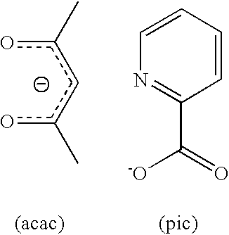
wherein the acac or the pic may be substituted at one or more of the carbon atoms with one or more of alkyl, alkenyl, alkynyl, alkylaryl, CN, CF3, CO2R, C(O)R, NR2, NO2, OR, halo, aryl, and heteroaryl. A preferred derivative of acac that may be used as a bidentate ligand is dpm: 
wherein the acac or the pic may be substituted at one or more of the carbon atoms with one or more of alkyl, alkenyl, alkynyl, alkylaryl, CN, CF3, CO2R, C(O)R, NR2, NO2, OR, halo, aryl, and heteroaryl. A preferred derivative of acac that may be used as a bidentate ligand is dpm:
The best choice for the A1, A2 ligand(s) will have a high triplet energy. This will give the resulting metal complex the highest possible triplet energy and the best exciton blocking character. While a low triplet energy ligand (e.g. 8-hydroxyquinolate has a triplet energy of 650 nm or 1.9 eV) will limit the exciton blocking abilities of a material it may not affect the materials ability to act as an electron blocker.
A further preferred embodiment, invention comprises the compound of the formula I in which m is 2 and n is 1, to give a compound of the formula II

wherein M, R1, R2, R3, R4, R5 R6, R7, A1, and A2 are as described for the compound of the formula I.
wherein M, R1, R2, R3, R4, R5 R6, R7, A1, and A2 are as described for the compound of the formula I.
According to compounds of the present invention, M can be any metal atom, including transition metals, lanthanides, actinides, main group metals, alkali metals and alkaline earth metals. In a preferred embodiment, M is a transition metal. In more preferred embodiments, M is a second or third row transition metal. In some embodiments, M is Ir, Os, Pt, Pb, Re, or Ru. In particularly preferred embodiments, M is Ir.
Another embodiment of the invention comprises the compound of the formula I in which m is 3 and n is 0, resulting in a compound of the formula III

wherein M is a metal;
wherein M is a metal;
-
- each of R1, R2, R3, R4, R5, R6, and R7 is, independently, H, alkyl, alkenyl, alkynyl, alkylaryl, CN, CF3, CxF2x+1, trifluorovinyl , CO2R, C(O)R, NR2, NO2, OR, halo, aryl, heteroaryl, substituted aryl, substituted heteroaryl or a heterocyclic group, and additionally, or alternatively, any one or more of R1 and R2, or R2 and R3, or R3 and R4, or R4 and R5 or R5 and R6, or R6 and R7 together form, independently, a fused 5- to 6-member cyclic group, wherein said cyclic group is cycloalkyl, cycloheteroalkyl, aryl, or heteroaryl, and wherein the fused 5- to 6-member cyclic group cyclic group may be optionally substituted with one or more of alkyl, alkenyl, alkynyl, alkylaryl, CN, CF3, CxF2x+1, trifluorovinyl, CO2R, C(O)R, NR2, NO2, OR, halo; and
- each R is independently H, alkyl, alkenyl, alkynyl, alkylaryl, and aryl.
One embodiment of the invention comprises the compound of the formula III in which R1, R2, R3, R4, R5, R6, and R7 are each H for use as electron blocking materials. For example, the unsubstituted iridium phenylpyrazole complex (e.g. Ir(ppz)3) is an effective electron blocker in OLEDs.

The estimated HOMO and LUMO levels of Irppz are summarized in FIG. 4. The energy levels scheme suggests that Irppz should make an excellent EBL.
The estimated HOMO and LUMO levels of Irppz are summarized in FIG. 4. The energy levels scheme suggests that Irppz should make an excellent EBL.
Unfortunately, devices prepared with Ir(ppz)3 generally have short device lifetimes. The device instability appears to be due to poor stability of the complex, during device operation. A paper by Pavlik (“Phototransposition Chemistry of 1-Phenylpyrazole. Experimental and Computational Studies” James W. Pavlik, Robert E. Connors, Douglas S. Burns, and Edyth M. Kurzweil, Journal of the American Chemical Society, 1993, vol. 115, 7645-7652) discusses the photochemical isomerization of N-phenylpyrazole and methyl-N-phenylpyrazoles to phenyl-imidazoles. The quantum efficiency of the isomerization reaction of N-phenylpyrazole is over 0.2 and increases to over 0.6 for compounds 4-methyl-N-phenylpyrazole and 5-methyl-N-phenylpyrazole. The methyl substitution in 3-methyl-N-phenylpyrazole leads to a decrease in the isomerization efficiency to less than 0.01. Without being limited by theory, it is believed that a similar isomerization may occur for Ir(ppz)3 and similar metal phenylpyrazole electron blockers. Such an isomerization of the N-phenylpyrazole to a phenyl-imidazole ligand, or a ring opened structure could lead to decomposition of the metal phenylpyrazole electron blocker. Substitution on the N-phenylpyrazole ligand, particularly at R1, may lead to a marked increase in the stability of metal phenylpyrazole electron blockers.
Thus, in a preferred embodiment, the devices of the present invention comprise an electron blocking layer, wherein the electron blocking layer comprises a compound of the formula II or formula III wherein R1 is a substituent other than H. In a further preferred embodiment, R1 is alkyl or aralkyl. In a particularly preferred embodiment, R1 is methyl.
In a further preferred embodiment, the devises of the present invention comprise an electron blocking layer, wherein the electron blocking layer comprises a material of the formula II or formula III wherein R2 and R3 are H to give a compound of the formula IIa or formula IIIa

wherein M is a metal;
wherein M is a metal;
-
- each A1 and A2 is, independently, a monodentate ligand; or A1 and A2 are covalently joined together to form a bidentate ligand;
- R1 is alkyl, alkenyl, alkynyl, alkylaryl, CN, CF3, CxF2x+1, trifluorovinyl, CO2R, C(O)R, NR2, NO2, OR, halo, aryl, heteroaryl, substituted aryl, substituted heteroaryl or a heterocyclic group;
- each of R4, R5, R6, and R7 is, independently, H, alkyl, alkenyl, alkynyl, alkylaryl, CN, CF3, CxF2x+1, trifluorovinyl, CO2R, C(O)R, NR2, NO2, OR, halo, aryl, heteroaryl, substituted aryl, substituted heteroaryl or a heterocyclic group, and additionally, or alternatively, any one or more of R4 and R5, or R5 and R6, or R6 and R7 together form, independently, a fused 5- to 6-member cyclic group, wherein said cyclic group is cycloalkyl, cycloheteroalkyl, aryl, or heteroaryl, and wherein the fused 5- to 6-member cyclic group cyclic group may be optionally substituted with one or more of alkyl, alkenyl, alkynyl, alkylaryl, CN, CE3, GF, trifluorovinyl, CO2R, C(O)R, NR2, NO2, OR, halo; and
- each R is independently H, alkyl, alkenyl, alkynyl, alkylaryl, and aryl.
In a preferred embodiment, the devices of the present invention comprise an electron blocking layer, wherein the electron blocking layer comprises a compound of the formula IIa or formula IIIa, wherein R1 is alkyl or aralkyl. In a particularly preferred embodiment, R1 is methyl.
While the present invention has been illustrated for R1-substituted N-phenylpyrazole compounds that have a reduced isomerization as compared with unsubstituted N-phenylpyrazole compounds, it is believed that compounds substituted instead at the R2 and/or R3 position might also have reduced isomerization. Thus, other embodiments of the present invention may include electron blocking layers comprising a compound of the formula IIa or formula IIIa, wherein R1 is hydrogen and at least one of R2 or R3 is other than hydrogen, in particular, at least one of R2 or R3 is alkyl or aralkyl.
In addition, while the present invention has been illustrated for substituted N-phenylpyrazole compounds that have a reduced isomerization as compared with unsubstituted N-phenylpyrazole compounds, wherein It is a particularly preferred metal, other metals may also be used wherein the chemical compound is represented by the following partial structure:

wherein M is a metal;
wherein M is a metal;
-
- each of R1, R2, R3, R4, R5, R6, and R7 is, independently, H, alkyl, alkenyl, alkynyl, alkylaryl, CN, CF3, CxF2x+1, trifluorovinyl, CO2R, C(O)R, NR2, NO2, OR, halo, aryl, heteroaryl, substituted aryl, substituted heteroaryl or a heterocyclic group, and additionally, or alternatively, any one or more of R1 and R2, or R2 and R3, or R3 and R4, or R4 and R5, or R5 and R6, or R6 and R7 together form, independently, a fused 5- to 6-member cyclic group, wherein said cyclic group is cycloalkyl, cycloheteroalkyl, aryl, or heteroaryl, and wherein the fused 5- to 6-member cyclic group cyclic group may be optionally substituted with one or more of alkyl, alkenyl, alkynyl, alkylaryl, CN, CF3, CxF2x+1, trifluorovinyl, CO2R, C(O)R, NR2, NO2, OR, halo; and
- each R is independently H, alkyl, alkenyl, alkynyl, alkylaryl, and aryl.
The term “halo” or “halogen” as used herein includes fluorine, chlorine, bromine and iodine.
The term “alkyl” as used herein contemplates both straight and branched chain alkyl radicals. Preferred alkyl groups are those containing from one to fifteen carbon atoms and includes methyl, ethyl, propyl, isopropyl, butyl, isobutyl, tert-butyl, and the like. Additionally, the alkyl group may be optionally substituted with one or more substituents selected from halo, CN, CO2R, C(O)R, NR2, cyclic-amino, NO2, and OR.
The term “cycloalkyl” as used herein contemplates cyclic alkyl radicals. Preferred cycloalkyl groups are those containing 3 to 7 carbon atoms and includes cyclopropyl, cyclopentyl, cyclohexyl, and the like. Additionally, the cycloalkyl group may be optionally substituted with one or more substituents selected from halo, CN, CO2R, C(O)R, NR2, cyclic-amino, NO2, and OR.
The term “alkenyl” as used herein contemplates both straight and branched chain alkene radicals. Preferred alkenyl groups are those containing two to fifteen carbon atoms. Additionally, the alkenyl group may be optionally substituted with one or more substituents selected from halo, CN, CO2R, C(O)R, NR2, cyclic-amino, NO2, and OR.
The term “alkynyl” as used herein contemplates both straight and branched chain alkyne radicals. Preferred alkyl groups are those containing two to fifteen carbon atoms. Additionally, the alkynyl group may be optionally substituted with one or more substituents selected from halo, CN, CO2R, C(O)R, NR2, cyclic-amino, NO2, and OR.
The term “alkylaryl” as used herein contemplates an alkyl group which has as a substituent an aromatic group. Additionally, the alkylaryl group may be optionally substituted on the aryl with one or more substituents selected from halo, CN, CO2R, C(O)R, NR2, cyclic-amino, NO2, and OR.
The term “heterocyclic group” as used herein contemplates non-aromatic cyclic radicals. Preferred heterocyclic groups are those containing 3 or 7 ring atoms which includes at least one hetero atom, and includes cyclic amines such as morpholino, piperdino, pyrrolidino, and the like, and cyclic ethers, such as tetrahydrofuran, tetrahydropyran, and the like.
The term “aryl” or “aromatic group” as used herein contemplates single-ring aromatic groups and polycyclic ring systems. The polycyclic rings may have two or more rings in which two carbons are common by two adjoining rings (the rings are “fused”) wherein at least one of the rings is aromatic, e.g., the other rings can be cycloalkyls, cycloalkenyls, aryl, heterocycles and/or heteroaryls.
The term “heteroaryl” as used herein contemplates single-ring hetero-aromatic groups that may include from one to three heteroatoms, for example, pyrrole, furan, thiophene, imidazole, oxazole, thiazole, triazole, pyrazole, pyridine, pyrazine and pyrimidine, and the like. The term heteroaryl also includes polycyclic hetero-aromatic systems having two or more rings in which two atoms are common to two adjoining rings (the rings are “fused”) wherein at least one of the rings is a heteroaryl, e.g., the other rings can be cycloalkyls, cycloalkenyls, aryl, heterocycles and/or heteroaryls.
It is understood that the various embodiments described herein are by way of example only, and are not intended to limit the scope of the invention. For example, many of the materials and structures described herein may be substituted with other materials and structures without deviating from the spirit of the invention. It is understood that various theories as to why the invention works are not intended to be limiting. For example, theories relating to charge transfer are not intended to be limiting.
Material Definitions:
As used herein, abbreviations refer to materials as follows:
| CBP: | 4,4′-N,N-dicarbazole-biphenyl |
| m- |
4,4′,4″-tris(3-methylphenylphenlyamino)triphenylamine |
| Alq3: | 8-tris-hydroxyquinoline aluminum |
| Bphen: | 4,7-diphenyl-1,10-phenanthroline |
| n-BPhen: | n-doped BPhen (doped with lithium) |
| F4-TCNQ: | tetrafluoro-tetracyano-quinodimethane |
| p-MTDATA: | p-doped m-MTDATA (doped with F4-TCNQ) |
| Ir(ppy)3: | tris(2-phenylpyridine)-iridium |
| Ir(ppz)3: | tris(1-phenylpyrazoloto,N,C(2′)iridium(III) |
| BCP: | 2,9-dimethyl-4,7-diphenyl-1,10-phenanthroline |
| TAZ: | 3-phenyl-4-(1′-naphthyl)-5-phenyl-1,2,4-triazole |
| CuPc: | copper phthalocyanine. |
| ITO: | indium tin oxide |
| NPD: | naphthyl-phenyl-diamine |
| TPD: | N,N′-bis(3-methylphenyl)-N,N′-bis-(phenyl)-benzidine |
| BAlq: | aluminum(III)bis(2-methyl-8-quinolinato)4- |
| phenylphenolate | |
| mCP: | 1,3-N,N-dicarbazole-benzene |
| DCM: | 4-(dicyanoethylene)-6-(4-dimethylaminostyryl-2- |
| methyl)-4H-pyran | |
| DMQA: | N,N′-dimethylquinacridone |
| PEDOT:PSS: | an aqueous dispersion of poly(3,4- |
| ethylenedioxythiophene) with | |
| polystyrenesulfonate (PSS) | |
| ppz2Ir(dpm): | Iridium(III) bis(1-phenylpyrazolato,N, C2′) (2,2,6,6- |
| tetramethyl-3,5-heptanedionato-O,O | |
| FPt1: | Platinum(II) (2-(4′,6′-difluorophenyl)pyridinato-N,C2′) |
| (2,4-pentanedionato-O,O) | |
| FPt2: | Platinum (II) (2-(4′,6′-difluorophenyl)pyridinato-N,C2′) |
| (2,6-dimethyl-3,5-heptanedionato-O,O) | |
Specific representative embodiments of the invention will now be described, including how such embodiments may be made. It is understood that the specific methods, materials, conditions, process parameters, apparatus and the like do not necessarily limit the scope of the invention.
Where available, solvents and reagents were purchased from Aldrich Chemical Company. The reagents were of the highest purity and used as received.
The ligand 2-(2,4-difluorophenyl)pyridine (F2ppy) was prepared by Suzuki coupling 2,4-difluorophenylboronic acid and 2-bromopyridine (Aldrich). The Pt(II) μ-dichloro-bridged dimer [(F2ppy)2Pt(μ-Cl)2Pt(F2ppy)2] was prepared by a modified method of Lewis. (Lohse, O. et al. Synlett. 1999, 1, 45-48). The dimer was treated with 3 equivalents of the chelating diketone ligand and 10 equivalents of Na2CO3. 2,6-dimethyl-3,5-heptanedione, and 6-methyl-2,4-heptanedione, were purchased from TCI. 3-Ethyl-2,4-pentandione was purchased from Aldrich. The solvent was removed under reduced pressure, and the compound purified chromatographically. The product was recrystallized from dichloromethane/methanol and then sublimed.
Irppz was prepared by dissolving Ir(acac)3 (3.0 g) and 1-phenylpyrazole (3.1 g) in 100 ml glycerol and refluxing for 12 hours under and inert atmosphere. After cooling the product was isolated by filtration and washed with several portions of distilled water, methanol, ether and hexanes and then vacuum dried. The crude product was then sublimed in a temperature gradient of 220-250° C. to give a pale yellow product (yield 58%).
(ppz)2Ir(dpm) was prepared by the following procedure. [(ppz)2IrCl]2, was treated with an excess of 2,2,5,5-tetramehtyl-heptanedione (i.e. dpm, 3 equivalents), and sodium carbonate (10 equivalents) in 2-ethoxyethanol. The slurry was refluxed was refluxed under an inert gas atmosphere for 12 hours. After cooling to room temperature, the cream colored precipitate was filtered off and was washed with water, followed by 2 portions of ether and hexane. The crude product was flash chromatographed using a silica:dichloromethane column, and sublimed to give a colorless solid. see Synthesis and Characterization of Phosphorescent Cyclometalated Iridium Complexes. Sergey Lamansky, Peter Djurovich, Drew Murphy, Feras Abdel-Razaq, Raymond Kwong, Irina Tsyba, Manfred Bortz, Becky Mui, Robert Bau, Mark E. Thompson, Inorganic Chemistry, 2001, 40(7), 1704-1711.
mCP was prepared by the palladium-catalyzed cross coupling of aryl halides and arylamines. (T. Yamamoto, M. Nishiyama, Y. Koie Tet. Lett., 1998, 39, 2367-2370).
Device Fabrication
Prior to device fabrication, indium tin oxide (ITO) on glass was patterned as 2 mm wide stripes (sheet resistance 20 Ω/□) The substrates were cleaned by sonication in soap solution, rinsing with deionized water, boiled in trichloroethylene, acetone and ethanol for 3-4 min in each solvent. After the cleaning procedure, the substrates were dried under an N2 flow followed by UV ozone treatment for 10 min.
Organic layers of the OLEDs were sequentially deposited by thermal evaporation from resistively heated tantalum boats onto the substrates, at room temperature, at a base pressure of ˜3-4×10⁻⁶ Torr, at 2.5 Å/s. The rate of a single-component layer was controlled with one Inficon thickness monitor located close to the substrate. For the two-component emissive layer the rate of the dopant was controlled with an additional crystal monitor located close to the dopant evaporation source. The additional monitor was not exposed to the major flow of the host, which allowed increasing the precision of the dopant concentration.
After deposition of the organic films, the chamber was vented and a shadow mask with 2 mm wide stripes was put onto the substrates across the ITO strips. The cathode consisting of 10 Å LiF followed by 1000-1500 Å of aluminum was deposited at 0.3-0.4 Å/s for LiF and 3-4 Å/s for aluminum. The OLEDs were formed as 2×2 mm squares at the intersections of ITO anode and Al cathode stripes.
The devices were characterized in the air within 2 h of fabrication. Current-voltage measurements were made with a Keithley source meter (model 2400). Light intensity was measured using a Newport model 1835 optical power meter and 818-UV Newport detector. EL spectra were measured with a Photon Technology International fluorimeter.
An OLED with the structure ITO/NPD(400 Å)/CBP:FPt2 8%(300 Å)/BCP(150 Å)/ALq3(200 Å)/LiF(10 Å)/Al(1000 Å) was fabricated (FIG. 5A). The device had predominantly NPD emission in the spectrum due to electron leakage into HTL (FIG. 6). The EL spectrum was voltage dependent and did not give stable color. As a result a low device efficiency (˜1%) was obtained.
A device was fabricated as described in example 1, except that a 200 Å thick electron-blocking layer of Ir(ppz)3 was introduced between the HTL and the emissive layer (FIG. 5B). With the introduction of the Irppz EBL is to the FPt based WOLED structure, the electron leakage into the NPD layer is eliminated. The electroluminescent spectra of the single dopant WOLEDs (using 8 wt % FPt2 in CBP), with and without Irppz EBL, are shown in FIG. 6. The device having the Irppz electron blocking layer gives an EL spectrum consistent with only dopant emission (i.e. no NPD emission is observed at any bias level) leading to a voltage independent, high quality white emission. The quantum efficiency of the device with an Irppz blocking layer is nearly double that of the device with no EBL (peak efficiency=1.9%).
An OLED device with the structure ITO/NPD(400 Å)/mCP:FPt1 16%(300 Å)/BCP(150 Å)/Alq3(200 Å)/LiF(10 ÅAl(1000 Å) was fabricated. This device had a NPD emission in the spectrum due to electron leakage into HTL (FIG. 9). The EL spectrum was voltage dependent and did not give stable color. A device efficiency of 3% was obtained (FIG. 8).
A device was fabricated as described in example 3 except that a 200 Å thick electron-blocking layer of Ir(ppz)3 was introduced between the HTL and the EL (FIG. 7). NPD emission was eliminated by the introduction of the EBL. The device efficiency increased to 6.5% (FIG. 8). The chart of the quantum efficiency shows that the over all OLED efficiency is 2 times greater for the device having the electron blocking layer compared to the device without the electron blocking layer. The EL spectra of this device and the device in example 3 are shown in FIG. 9. As seen in the electroluminescent spectra, without the electron blocking layer, emission occurs from both the HTL (α-NPD) and the emissive layer. For the device having an electron blocking layer, emission is confined to the doped emissive layer and emission from the α-NPD is not observed. The IV characteristics are nearly identical for the two devices (FIG. 10). This confirms that Ir(ppz)3 EBL is a good hole-transporter and does not impede the current through the device.
An OLED with the structure ITO/NPD(400 Å)/CBP:FPt1 6%(300 Å)/BCP(150 Å)/AlLq3(200 Å)/LiF(10 Å)/Al(1000 Å) was fabricated. It had predominantly NPD emission in the EL spectrum due to electron leakage (FIG. 13). As a result a low device efficiency (˜1%) was obtained (FIG. 12 )
A device was fabricated as described in example 5, except that a 200 Å thick electron-blocking layer of (ppz)2Ir(dpm) was introduced between the HTL and the EL. The EL, spectrum of this device contained only dopant (FPt) emission. (see FIG. 13). The efficiency of this device was almost 3 times higher (about 3%) due to recombination occurring only in the ELM (see FIG. 12). The EL spectra of this device at different bias levels are shown in FIG. 14. They are nearly voltage independent. So the introduction of (ppz)2Ir(dpm) EBL improved both efficiency and color stability of the device because of the successful confinement of electrons in the EL by the EBL.
While the present invention is described with respect to particular examples and preferred embodiments, it is understood that the present invention is not limited to these examples and embodiments. The present invention as claimed therefore includes variations from the particular examples and preferred embodiments described herein, as will be apparent to one of skill in the art.
Claims (26)
1. An organic light emitting device, comprising an electron blocking layer disposed adjacent to an emissive layer, wherein the electron blocking layer comprises a compound of the formula I

wherein M is a metal;
each A1 and A2 is, independently, a monodentate ligand; or A1 and A2 are covalently joined together to form a bidentate ligand;
each of R1, R2, R3, R4, R5, R6, and R7 is, independently, H, alkyl, alkenyl, alkynyl, alkylaryl, CN, CF3, CxF2x+1, trifluorovinyl, CO2R, C(O)R, NR2, NO2, OR, halo, aryl, heteroaryl, substituted aryl, substituted heteroaryl or a heterocyclic group, and additionally, or alternatively, any one or more of R1 and R2, or R2 and R3, or R3 and R4, or R4 and R5, or R5 and R6, or R6 and R7 together form, independently, a fused 5- to 6-member cyclic group, wherein said cyclic group is cycloalkyl, cycloheteroalkyl, aryl, or heteroaryl, and wherein the fused 5- to 6-member cyclic group may be optionally substituted with one or more of alkyl, alkenyl, alkynyl, alkylaryl, CN, CF3, CxF2x+1, trifluorovinyl, CO2R, C(O)R, NR2, NO2, OR, halo;
each R is independently H, alkyl, alkenyl, alkynyl, alkylaryl, and aryl;
m is 1, 2, or 3; and
n is 0, 1, or 2,
wherein m+n equals 3.
2. The organic light emitting device of claim 1 , wherein the electron blocking layer comprises a compound of the formula I, wherein R2 and R3 are H.
3. The organic light emitting device of claim 2 , wherein the electron blocking layer comprises a compound of the formula I, wherein R1 is alkyl or aralkyl.
4. The organic light emitting device of claim 2 , wherein the electron blocking layer comprises a compound of the formula I, wherein R1 is methyl.
5. The organic light emitting device of claim 2 , wherein the electron blocking layer comprises a compound of the formula I, wherein m is 2 and n is 1.
6. The organic light emitting device of claim 5 , wherein the electron blocking layer comprises a compound of the formula I, wherein M is Ir.
7. The organic light emitting device of claim 1 , wherein the electron blocking layer comprises a compound of the formula

8. An organic light emitting device, comprising an electron blocking layer disposed adjacent to an emissive layer, wherein the electron blocking layer comprises a compound of the formula III

wherein M is a metal;
each of R1, R2, R3, R4, R5, R6, and R7 is, independently, H, alkyl, alkenyl, alkynyl, alkylaryl, CN, CF3, CxF2x+1, trifluorovinyl, CO2R, C(O)R, NR2, NO2, OR, halo, aryl, heteroaryl, substituted aryl, substituted heteroaryl or a heterocyclic group, and additionally, or alternatively, any one or more of R1 and R2, or R2 and R3, or R3 and R4, or R4 and R5, or R5 and R6, or R6 and R7 together form, independently, a fused 5- to 6-member cyclic group, wherein said cyclic group is cycloalkyl, cycloheteroalkyl, aryl, or heteroaryl, and wherein the fused 5- to 6-member cyclic group may be optionally substituted with one or more of alkyl, alkenyl, alkynyl, alkylaryl, CN, CF3, CxF2x+1, trifluorovinyl, CO2R, C(O)R, NR2, NO2, OR, halo; and
each R is independently H, alkyl, alkenyl, alkynyl, alkylaryl, and aryl.
9. The organic light emitting device of claim 8 , wherein the electron blocking layer comprises a compound of the formula III, wherein R2 and R3 are H.
10. The organic light emitting device of claim 9 , wherein the electron blocking layer comprises a compound of the formula III, wherein R1 is alkyl or aralkyl.
11. The organic light emitting device of claim 9 , wherein the electron blocking layer comprises a compound of the formula III, wherein R1 is methyl.
12. The organic light emitting device of claim 11 , wherein the electron blocking layer comprises a compound of the formula III, wherein M is Ir.
13. The organic light emitting device of claim 8 , wherein the electron blocking layer comprises a compound of the formula

14. An organic light emitting device comprising
an anode;
a hole transporting layer;
an electron blocking layer comprising an electron blocking material;
an emissive layer disposed adjacent to the electron blocking layer;
an electron transporting layer; and
a cathode;
wherein the electron blocking material comprises a compound of the formula I

wherein M is a metal;
each A1 and A2 is, independently, a monodentate ligand; or A1 and A2 are covalently joined together to form a bidentate ligand;
each of R1, R2, R3, R4, R5, R6, and R7 is, independently, H, alkyl, alkenyl, alkynyl, alkylaryl, CN, CF3, CxF2x+1, trifluorovinyl, CO2R, C(O)R, NR2, NO2, OR, halo, aryl, heteroaryl, substituted aryl, substituted heteroaryl or a heterocyclic group, and additionally, or alternatively, any one or more of R1 and R2, or R2 and R3, or R3 and R4, or R4 and R5, or R5 and R6, or R6 and R7 together form, independently, a fused 5- to 6-member cyclic group, wherein said cyclic group is cycloalkyl, cycloheteroalkyl, aryl, or heteroaryl, and wherein the fused 5- to 6-member cyclic group may be optionally substituted with one or more of alkyl, alkenyl, alkynyl, alkylaryl, CN, CF3, CxF2x+1, trifluorovinyl, CO2R, C(O)R, NR2, NO2, OR, halo;
each R is independently H, alkyl, alkenyl, alkynyl, alkylaryl, and aryl;
m is 1, 2, or 3; and
n is 0, 1, or 2,
wherein m+n equals 3.
15. The organic light emitting device of claim 14 , wherein the electron blocking layer comprises a compound of the formula I, wherein R2 and R3 are H.
16. The organic light emitting device of claim 15 , wherein the electron blocking layer comprises a compound of the formula I, wherein R1 is alkyl or aralkyl.
17. The organic light emitting device of claim 15 , wherein the electron blocking layer comprises a compound of the formula I, wherein R1 is methyl.
18. The organic light emitting device of claim 14 , wherein the electron blocking layer comprises a compound of the formula I, wherein m is 2 and n is 1.
19. The organic light emitting device of claim 18 , wherein the electron blocking layer comprises a compound of the formula I, wherein M is Ir.
20. The organic light emitting device of claim 14 , wherein the electron blocking layer comprises a compound of the formula

21. The organic light emitting device of claim 14 , wherein the electron blocking layer comprises a compound of the formula

wherein M is a metal;
each of R1, R2, R3, R4, R5, R6, and R7 is, independently, H, alkyl, alkenyl, alkynyl, alkylaryl, CN, CF3, CxF2x+1, trifluorovinyl, CO2R, C(O)R, NR2, NO2, OR, halo, aryl, heteroaryl, substituted aryl, substituted heteroaryl or a heterocyclic group, and additionally, or alternatively, any one or more of R1 and R2, or R2 and R3, or R3 and R4, or R4 and R5, or R5 and R6, or R6 and R7 together form, independently, a fused 5- to 6-member cyclic group, wherein said cyclic group is cycloalkyl, cycloheteroalkyl, aryl, or heteroaryl, and wherein the fused 5- to 6-member cyclic group may be optionally substituted with one or more of alkyl, alkenyl, alkynyl, alkylaryl, CN, CF3, CxF2x+1, trifluorovinyl CO2R, C(O)R, NR2, NO2, OR, halo; and
each R is independently H, alkyl, alkenyl, alkynyl, alkylaryl, and aryl.
22. The organic light emitting device of claim 21 , wherein the electron blocking layer comprises a compound of the formula III, wherein R2 and R3 are H.
23. The organic light emitting device of claim 22 , wherein the electron blocking layer comprises a compound of the formula III, wherein R1 is alkyl or aralkyl.
24. The organic light emitting device of claim 23 , wherein the electron blocking layer comprises a compound of the formula III, wherein R1 is methyl.
25. The organic light emitting device of claim 24 , wherein the electron blocking layer comprises a compound of the formula III, wherein M is Ir.
26. The organic light emitting device of claim 14 , wherein the electron blocking layer comprises a compound of the formula

Priority Applications (2)
| Application Number | Priority Date | Filing Date | Title |
|---|---|---|---|
| US10/402,684 US6951694B2 (en) | 2002-03-29 | 2003-03-28 | Organic light emitting devices with electron blocking layers |
| US11/230,851 US7553557B2 (en) | 2002-03-29 | 2005-09-19 | Organic light emitting devices with electron blocking layers |
Applications Claiming Priority (4)
| Application Number | Priority Date | Filing Date | Title |
|---|---|---|---|
| US36849602P | 2002-03-29 | 2002-03-29 | |
| US10/112,257 US6869695B2 (en) | 2001-12-28 | 2002-03-29 | White light emitting OLEDs from combined monomer and aggregate emission |
| US10/328,914 US6863997B2 (en) | 2001-12-28 | 2002-12-24 | White light emitting OLEDs from combined monomer and aggregate emission |
| US10/402,684 US6951694B2 (en) | 2002-03-29 | 2003-03-28 | Organic light emitting devices with electron blocking layers |
Related Parent Applications (2)
| Application Number | Title | Priority Date | Filing Date |
|---|---|---|---|
| US10/112,257 Continuation-In-Part US6869695B2 (en) | 2001-12-28 | 2002-03-29 | White light emitting OLEDs from combined monomer and aggregate emission |
| US10/328,914 Continuation-In-Part US6863997B2 (en) | 2001-12-28 | 2002-12-24 | White light emitting OLEDs from combined monomer and aggregate emission |
Related Child Applications (1)
| Application Number | Title | Priority Date | Filing Date |
|---|---|---|---|
| US11/230,851 Continuation US7553557B2 (en) | 2002-03-29 | 2005-09-19 | Organic light emitting devices with electron blocking layers |
Publications (2)
| Publication Number | Publication Date |
|---|---|
| US20040048101A1 US20040048101A1 (en) | 2004-03-11 |
| US6951694B2 true US6951694B2 (en) | 2005-10-04 |
Family
ID=31998935
Family Applications (2)
| Application Number | Title | Priority Date | Filing Date |
|---|---|---|---|
| US10/402,684 Expired - Lifetime US6951694B2 (en) | 2002-03-29 | 2003-03-28 | Organic light emitting devices with electron blocking layers |
| US11/230,851 Expired - Lifetime US7553557B2 (en) | 2002-03-29 | 2005-09-19 | Organic light emitting devices with electron blocking layers |
Family Applications After (1)
| Application Number | Title | Priority Date | Filing Date |
|---|---|---|---|
| US11/230,851 Expired - Lifetime US7553557B2 (en) | 2002-03-29 | 2005-09-19 | Organic light emitting devices with electron blocking layers |
Country Status (1)
| Country | Link |
|---|---|
| US (2) | US6951694B2 (en) |
Cited By (52)
| Publication number | Priority date | Publication date | Assignee | Title |
|---|---|---|---|---|
| US20040183082A1 (en) * | 2003-03-17 | 2004-09-23 | Hiroko Yamazaki | Light emitting element and light emitting device |
| US20040202893A1 (en) * | 2003-04-09 | 2004-10-14 | Hiroko Abe | Electroluminescent element and light-emitting device |
| US20040213308A1 (en) * | 2003-04-23 | 2004-10-28 | Hiroko Abe | Laser oscillator |
| US20050212003A1 (en) * | 2004-03-24 | 2005-09-29 | Hitachi Displays, Ltd. | Organic light-emitting display device |
| US20060024526A1 (en) * | 2002-03-29 | 2006-02-02 | Thompson Mark E | Organic light emitting devices with electron blocking layers |
| US20060175957A1 (en) * | 2003-07-23 | 2006-08-10 | Konica Minolta Holdings, Inc. | Organic electroluminescent device, illuminating device and display |
| US20070064173A1 (en) * | 2005-09-20 | 2007-03-22 | Au Optronics Corporation | Double-Sided Liquid Crystal Display |
| US20070126962A1 (en) * | 2005-12-05 | 2007-06-07 | Semiconductor Energy Laboratory Co., Ltd. | Liquid crystal display device |
| US20080026477A1 (en) * | 2006-07-28 | 2008-01-31 | General Electric Company | Method for preparing polymeric organic iridium compositions |
| US20080227230A1 (en) * | 2005-02-15 | 2008-09-18 | Samsung Electronics Co., Ltd. | Quantum dot vertical cavity surface emitting laser and fabrication method of the same |
| US20080315753A1 (en) * | 2007-06-20 | 2008-12-25 | Liang-Sheng Liao | Phosphorescent oled having double exciton-blocking layers |
| US20090134383A1 (en) * | 2005-04-22 | 2009-05-28 | Semiconductor Energy Laboratory Co, Ltd | Electrode for Organic Transistor, Organic Transistor, and Semiconductor Device |
| US20090159962A1 (en) * | 2007-12-20 | 2009-06-25 | Samsung Electronics Co., Ltd. | Non-Volatile Memory Devices |
| US20090174315A1 (en) * | 2006-02-07 | 2009-07-09 | Sumitomo Chemical Company Limited | Organic electroluminescent element |
| US20090179549A1 (en) * | 2003-04-07 | 2009-07-16 | Semiconductor Energy Laboratory Co., Ltd. | Electronic display including a light-emitting element and a color filter sandwiched between two polarizers |
| US7738055B2 (en) | 2006-01-31 | 2010-06-15 | Semiconductor Energy Laboratory Co., Ltd. | Display device having stacked polarizers that differ in degrees of light absorbing bands and that are between a pair of protective layers such that no protective layer is located between the stacked polarizers |
| US7804560B2 (en) | 2005-12-28 | 2010-09-28 | Semiconductor Energy Laboratory Co., Ltd. | Display device |
| US7808164B2 (en) | 2005-12-22 | 2010-10-05 | Semiconductor Energy Laboratory Co., Ltd. | Display device |
| US20100301382A1 (en) * | 2009-05-29 | 2010-12-02 | Semiconductor Energy Laboratory Co., Ltd. | Light-Emitting Element, Light-Emitting Device, Lighting Device, and Electronic Appliance |
| US20100301383A1 (en) * | 2009-05-29 | 2010-12-02 | Semiconductor Energy Laboratory Co., Ltd. | Light-Emitting Element, Light-Emitting Device, and Method for Manufacturing the Same |
| US7864268B2 (en) | 2006-02-24 | 2011-01-04 | Semiconductor Energy Laboratory Co., Ltd. | Display device with stack of polarizers having wavelength distributions of extinction coefficient of absorption axes |
| US7956957B2 (en) | 2006-02-24 | 2011-06-07 | Semiconductor Energy Laboratory Co., Ltd. | Display device |
| US8405800B2 (en) | 2006-02-02 | 2013-03-26 | Semiconductor Energy Laboratory Co., Ltd. | Display device with stacked polarizers |
| US8486543B2 (en) | 2009-12-01 | 2013-07-16 | Semiconductor Energy Laboratory Co., Ltd. | Light-emitting element, light-emitting device, electronic device, and lighting device |
| US8736157B2 (en) | 2011-04-07 | 2014-05-27 | Semiconductor Energy Laboratory Co., Ltd. | Light-emitting element |
| US8853680B2 (en) | 2011-03-30 | 2014-10-07 | Semiconductor Energy Laboratory Co., Ltd. | Light-emitting element |
| US8994013B2 (en) | 2012-05-18 | 2015-03-31 | Semiconductor Energy Laboratory Co., Ltd. | Light-emitting element, light-emitting device, display device, electronic device, and lighting device |
| US8994263B2 (en) | 2011-02-16 | 2015-03-31 | Semiconductor Energy Laboratory Co., Ltd. | Light-emitting element |
| US9059430B2 (en) | 2012-03-14 | 2015-06-16 | Semiconductor Energy Laboratory Co., Ltd. | Light-emitting element, light-emitting device, electronic device, and lighting device |
| US9065066B2 (en) | 2012-04-13 | 2015-06-23 | Semiconductor Energy Laboratory Co., Ltd. | Light-emitting element, light-emitting device, electronic device, and lighting device |
| US9088002B2 (en) | 2011-02-11 | 2015-07-21 | Semiconductor Energy Laboratory Co., Ltd. | Light-emitting device and manufacturing method thereof |
| US9142710B2 (en) | 2012-08-10 | 2015-09-22 | Semiconductor Energy Laboratory Co., Ltd. | Light-emitting element, light-emitting device, display device, electronic device, and lighting device |
| US9159942B2 (en) | 2012-04-20 | 2015-10-13 | Semiconductor Energy Laboratory Co., Ltd. | Light-emitting element, light-emitting device, electronic appliance, and lighting device |
| US9175213B2 (en) | 2011-03-23 | 2015-11-03 | Semiconductor Energy Laboratory Co., Ltd. | Light-emitting element |
| US9299944B2 (en) | 2012-04-13 | 2016-03-29 | Semiconductor Energy Laboratory Co., Ltd. | Light-emitting element, light-emitting device, electronic device, and lighting device |
| US9391289B2 (en) | 2012-04-06 | 2016-07-12 | Semiconductor Energy Laboratory Co., Ltd. | Light-emitting device, electronic device and light device each comprising light-emitting layer with mixed organic compounds capable of forming an exciplex |
| US9543537B2 (en) | 2010-11-19 | 2017-01-10 | Alliance For Sustainable Energy, Llc | Solution processed metal oxide thin film hole transport layers for high performance organic solar cells |
| US9604928B2 (en) | 2011-02-16 | 2017-03-28 | Semiconductor Energy Laboratory Co., Ltd. | Light-emitting element |
| US9660211B2 (en) | 2012-08-03 | 2017-05-23 | Semiconductor Energy Laboratory Co., Ltd. | Light-emitting element, light-emitting device, display device, electronic appliance, and lighting device |
| US9859515B2 (en) | 2013-03-07 | 2018-01-02 | Alliance For Sustainable Energy, Llc | Methods for producing thin film charge selective transport layers |
| US10074815B2 (en) * | 2015-03-31 | 2018-09-11 | The Regents Of The University Of Michigan | Organic electroluminescent devices |
| US10096658B2 (en) | 2016-04-22 | 2018-10-09 | Semiconductor Energy Laboratory Co., Ltd. | Light-emitting element, display device, electronic device, and lighting device |
| US20190115551A1 (en) * | 2017-10-16 | 2019-04-18 | Boe Technology Group Co., Ltd. | Oled device, method of manufacturing the same, and display device |
| US10756286B2 (en) | 2016-05-06 | 2020-08-25 | Semiconductor Energy Laboratory Co., Ltd. | Light-emitting element, display device, electronic device, and lighting device |
| US10998516B2 (en) | 2016-05-06 | 2021-05-04 | Semiconductor Energy Laboratory Co., Ltd. | Light-emitting element, display device, electronic device, and lighting device |
| US11072623B2 (en) | 2015-07-21 | 2021-07-27 | Semiconductor Energy Laboratory Co., Ltd. | Light-emitting element, display device, electronic device, and lighting device |
| US11362279B2 (en) | 2012-08-31 | 2022-06-14 | Idemitsu Kosan Co., Ltd. | Aromatic amine derivative, and organic electroluminescent element using same |
| US11637263B2 (en) | 2017-11-02 | 2023-04-25 | Semiconductor Energy Laboratory Co., Ltd. | Light-emitting element, display device, electronic device, and lighting device each including TADF organic compound |
| US11730007B2 (en) | 2012-08-03 | 2023-08-15 | Semiconductor Energy Laboratory Co., Ltd. | Light-emitting element |
| US11950497B2 (en) | 2018-03-07 | 2024-04-02 | Semiconductor Energy Laboratory Co., Ltd. | Light-emitting element, display device, electronic device, organic compound, and lighting device |
| US11991890B2 (en) | 2016-05-20 | 2024-05-21 | Semiconductor Energy Laboratory Co., Ltd. | Light-emitting element, display device, electronic device, and lighting device |
| US12545834B2 (en) | 2018-07-11 | 2026-02-10 | Semiconductor Energy Laboratory Co., Ltd. | Light-emitting device, display device, electronic device, organic compound, and lighting device |
Families Citing this family (41)
| Publication number | Priority date | Publication date | Assignee | Title |
|---|---|---|---|---|
| KR100490539B1 (en) * | 2002-09-19 | 2005-05-17 | 삼성에스디아이 주식회사 | Organic electroluminescence device and manufacturing method thereof |
| US20040096570A1 (en) * | 2002-11-15 | 2004-05-20 | Michael Weaver | Structure and method of fabricating organic devices |
| US6982179B2 (en) * | 2002-11-15 | 2006-01-03 | University Display Corporation | Structure and method of fabricating organic devices |
| EP1606296B1 (en) | 2003-03-24 | 2009-08-05 | University Of Southern California | PHENYL-PYRAZOLE COMPLEXES OF Ir |
| JP4198654B2 (en) * | 2003-08-07 | 2008-12-17 | 三星エスディアイ株式会社 | Iridium compound and organic electroluminescence device employing the same |
| US20050048314A1 (en) * | 2003-08-28 | 2005-03-03 | Homer Antoniadis | Light emitting polymer devices with improved efficiency and lifetime |
| US7101631B2 (en) * | 2003-12-05 | 2006-09-05 | Eastman Kodak Company | Organic element for electroluminescent devices |
| US7597967B2 (en) * | 2004-12-17 | 2009-10-06 | Eastman Kodak Company | Phosphorescent OLEDs with exciton blocking layer |
| US20070181874A1 (en) * | 2004-12-30 | 2007-08-09 | Shiva Prakash | Charge transport layers and organic electron devices comprising same |
| TWI255667B (en) * | 2005-04-21 | 2006-05-21 | Au Optronics Corp | Organic electroluminescent device and manufacturing method thereof and flat display device using the same |
| TWI279165B (en) * | 2005-08-09 | 2007-04-11 | Au Optronics Corp | White organic light emitting diode |
| JP2007073500A (en) * | 2005-08-11 | 2007-03-22 | Semiconductor Energy Lab Co Ltd | Light emitting element, light emitting device and electronic device |
| KR100729089B1 (en) * | 2005-08-26 | 2007-06-14 | 삼성에스디아이 주식회사 | OLED display device and manufacturing method thereof |
| WO2007095061A2 (en) * | 2006-02-09 | 2007-08-23 | Qd Vision, Inc. | Device including semiconductor nanocrystals and a layer including a doped organic material and methods |
| JP5672648B2 (en) | 2006-03-17 | 2015-02-18 | コニカミノルタ株式会社 | Organic electroluminescence element, display device and lighting device |
| EP3081619A1 (en) | 2006-03-23 | 2016-10-19 | Konica Minolta Holdings, Inc. | Organic electroluminescent element, display device and illuminating device |
| KR101513311B1 (en) | 2006-09-29 | 2015-04-22 | 유니버시티 오브 플로리다 리서치 파운데이션, 인크. | Method and apparatus for infrared detection and display |
| US8119255B2 (en) | 2006-12-08 | 2012-02-21 | Universal Display Corporation | Cross-linkable iridium complexes and organic light-emitting devices using the same |
| TWI558716B (en) * | 2006-12-08 | 2016-11-21 | 環球展覽公司 | Cross-linkable iridium complexes and organic light-emitting devices using the same |
| WO2009030981A2 (en) * | 2006-12-28 | 2009-03-12 | Universal Display Corporation | Long lifetime phosphorescent organic light emitting device (oled) structures |
| JPWO2008123178A1 (en) * | 2007-03-23 | 2010-07-15 | 出光興産株式会社 | Organic EL device |
| KR101375331B1 (en) * | 2007-06-22 | 2014-03-18 | 삼성디스플레이 주식회사 | White organic light emitting device and display apparatus and lighting apparatus comprising the same |
| JPWO2009008344A1 (en) * | 2007-07-07 | 2010-09-09 | 出光興産株式会社 | Organic EL device |
| US8896201B2 (en) | 2008-02-19 | 2014-11-25 | Samsung Display Co., Ltd. | Organic light emitting device |
| KR100922757B1 (en) | 2008-02-19 | 2009-10-21 | 삼성모바일디스플레이주식회사 | Organic light emitting device with improved lifespan |
| DE102008056688A1 (en) | 2008-11-11 | 2010-05-12 | Merck Patent Gmbh | Materials for organic electroluminescent devices |
| US8288187B2 (en) | 2010-01-20 | 2012-10-16 | Universal Display Corporation | Electroluminescent devices for lighting applications |
| SG185375A1 (en) | 2010-05-24 | 2012-12-28 | Univ Florida | Method and apparatus for providing a charge blocking layer on an infrared up-conversion device |
| MX2013005780A (en) * | 2010-11-23 | 2013-06-28 | Nanoholdings Llc | INFRARED PHOTODETECTORS WITH HIGH CAPACITY OF DETECTION IN LOW DRIVE VOLTAGE. |
| BR112013033122A2 (en) | 2011-06-30 | 2017-01-24 | Nanoholdings Llc | method and apparatus for detecting gain infrared radiation |
| US9118017B2 (en) * | 2012-02-27 | 2015-08-25 | Universal Display Corporation | Host compounds for red phosphorescent OLEDs |
| CN102659847B (en) * | 2012-04-17 | 2015-03-25 | 西安近代化学研究所 | Organic iridium complex |
| WO2014050417A1 (en) * | 2012-09-25 | 2014-04-03 | コニカミノルタ株式会社 | Organic electroluminescent element, lighting device, and display device |
| CN107636431A (en) | 2015-06-11 | 2018-01-26 | 佛罗里达大学研究基金会有限公司 | Single dispersing IR absorbs nano particle and associated method and device |
| KR102504124B1 (en) | 2015-07-31 | 2023-02-28 | 삼성디스플레이 주식회사 | Organic light emitting device |
| KR102520026B1 (en) | 2015-12-30 | 2023-04-07 | 엘지디스플레이 주식회사 | Organic light emitting diode |
| CN109427985B (en) * | 2017-08-31 | 2019-12-24 | 昆山国显光电有限公司 | Organic electroluminescent device and display device |
| US11046886B2 (en) * | 2017-09-14 | 2021-06-29 | Sumitomo Chemical Company, Limited | Method for producing liquid composition |
| KR102772128B1 (en) * | 2018-12-13 | 2025-02-21 | 엘지디스플레이 주식회사 | Delayed fluorescence compound, and Organic light emitting diode and Organic light emitting display device including the same |
| KR102846643B1 (en) * | 2020-11-09 | 2025-08-18 | 삼성디스플레이 주식회사 | Luminescence device and display device having the same |
| RO137484A0 (en) | 2022-10-12 | 2023-05-30 | Institutul Naţional De Cercetare Dezvoltare Pentru Fizica Materialelor (Incdfm) | Diode-like multilayer organic device on a transparent flexible substrate, based on electrospun polymeric fibers and organometallic compounds and process for manufacturing the same |
Citations (27)
| Publication number | Priority date | Publication date | Assignee | Title |
|---|---|---|---|---|
| US4769292A (en) | 1987-03-02 | 1988-09-06 | Eastman Kodak Company | Electroluminescent device with modified thin film luminescent zone |
| US5247190A (en) | 1989-04-20 | 1993-09-21 | Cambridge Research And Innovation Limited | Electroluminescent devices |
| US5703436A (en) | 1994-12-13 | 1997-12-30 | The Trustees Of Princeton University | Transparent contacts for organic devices |
| US5707745A (en) | 1994-12-13 | 1998-01-13 | The Trustees Of Princeton University | Multicolor organic light emitting devices |
| US5834893A (en) | 1996-12-23 | 1998-11-10 | The Trustees Of Princeton University | High efficiency organic light emitting devices with light directing structures |
| US5844363A (en) | 1997-01-23 | 1998-12-01 | The Trustees Of Princeton Univ. | Vacuum deposited, non-polymeric flexible organic light emitting devices |
| US6013538A (en) | 1997-11-24 | 2000-01-11 | The Trustees Of Princeton University | Method of fabricating and patterning OLEDs |
| US6013982A (en) | 1996-12-23 | 2000-01-11 | The Trustees Of Princeton University | Multicolor display devices |
| US6087196A (en) | 1998-01-30 | 2000-07-11 | The Trustees Of Princeton University | Fabrication of organic semiconductor devices using ink jet printing |
| US6091195A (en) | 1997-02-03 | 2000-07-18 | The Trustees Of Princeton University | Displays having mesa pixel configuration |
| US6097147A (en) | 1998-09-14 | 2000-08-01 | The Trustees Of Princeton University | Structure for high efficiency electroluminescent device |
| US20010019782A1 (en) * | 1999-12-27 | 2001-09-06 | Tatsuya Igarashi | Light-emitting material comprising orthometalated iridium complex, light-emitting device, high efficiency red light-emitting device, and novel iridium complex |
| US6294398B1 (en) | 1999-11-23 | 2001-09-25 | The Trustees Of Princeton University | Method for patterning devices |
| US6303238B1 (en) | 1997-12-01 | 2001-10-16 | The Trustees Of Princeton University | OLEDs doped with phosphorescent compounds |
| US20010053462A1 (en) | 2000-05-02 | 2001-12-20 | Masayuki Mishima | Light-emitting device |
| US6337102B1 (en) | 1997-11-17 | 2002-01-08 | The Trustees Of Princeton University | Low pressure vapor phase deposition of organic thin films |
| US20020025419A1 (en) | 1999-06-08 | 2002-02-28 | City University Of Hong Kong | White and colored organic electroluminescent devices using single emitting material by novel color change technique |
| US20020071963A1 (en) | 2000-12-13 | 2002-06-13 | Sanyo Electric Co., Ltd. | Organic light emitting device |
| US6420031B1 (en) | 1997-11-03 | 2002-07-16 | The Trustees Of Princeton University | Highly transparent non-metallic cathodes |
| US20020125818A1 (en) | 2000-10-04 | 2002-09-12 | Mitsubishi Chemical Corporation | Organic electroluminescent device |
| US6469437B1 (en) | 1997-11-03 | 2002-10-22 | The Trustees Of Princeton University | Highly transparent organic light emitting device employing a non-metallic cathode |
| US20020182441A1 (en) | 2000-08-11 | 2002-12-05 | Trustee Of Princeton University | Organometallic compounds and emission-shifting organic electrophosphorescence |
| US20020197511A1 (en) | 2001-05-16 | 2002-12-26 | D'andrade Brian | High efficiency multi-color electro-phosphorescent OLEDS |
| US20030059647A1 (en) * | 2001-08-29 | 2003-03-27 | Thompson Mark E. | Organic light emitting devices having carrier transporting layers comprising metal complexes |
| US20030068528A1 (en) * | 2001-08-29 | 2003-04-10 | Thompson Mark E. | Organic light emitting devices having carrier blocking layers comprising metal complexes |
| US20030230980A1 (en) | 2002-06-18 | 2003-12-18 | Forrest Stephen R | Very low voltage, high efficiency phosphorescent oled in a p-i-n structure |
| US6696177B1 (en) | 2000-08-30 | 2004-02-24 | Eastman Kodak Company | White organic electroluminescent devices with improved stability and efficiency |
Family Cites Families (1)
| Publication number | Priority date | Publication date | Assignee | Title |
|---|---|---|---|---|
| US6951694B2 (en) * | 2002-03-29 | 2005-10-04 | The University Of Southern California | Organic light emitting devices with electron blocking layers |
-
2003
- 2003-03-28 US US10/402,684 patent/US6951694B2/en not_active Expired - Lifetime
-
2005
- 2005-09-19 US US11/230,851 patent/US7553557B2/en not_active Expired - Lifetime
Patent Citations (29)
| Publication number | Priority date | Publication date | Assignee | Title |
|---|---|---|---|---|
| US4769292A (en) | 1987-03-02 | 1988-09-06 | Eastman Kodak Company | Electroluminescent device with modified thin film luminescent zone |
| US5247190A (en) | 1989-04-20 | 1993-09-21 | Cambridge Research And Innovation Limited | Electroluminescent devices |
| US5703436A (en) | 1994-12-13 | 1997-12-30 | The Trustees Of Princeton University | Transparent contacts for organic devices |
| US5707745A (en) | 1994-12-13 | 1998-01-13 | The Trustees Of Princeton University | Multicolor organic light emitting devices |
| US5834893A (en) | 1996-12-23 | 1998-11-10 | The Trustees Of Princeton University | High efficiency organic light emitting devices with light directing structures |
| US6013982A (en) | 1996-12-23 | 2000-01-11 | The Trustees Of Princeton University | Multicolor display devices |
| US5844363A (en) | 1997-01-23 | 1998-12-01 | The Trustees Of Princeton Univ. | Vacuum deposited, non-polymeric flexible organic light emitting devices |
| US6091195A (en) | 1997-02-03 | 2000-07-18 | The Trustees Of Princeton University | Displays having mesa pixel configuration |
| US6420031B1 (en) | 1997-11-03 | 2002-07-16 | The Trustees Of Princeton University | Highly transparent non-metallic cathodes |
| US6469437B1 (en) | 1997-11-03 | 2002-10-22 | The Trustees Of Princeton University | Highly transparent organic light emitting device employing a non-metallic cathode |
| US6337102B1 (en) | 1997-11-17 | 2002-01-08 | The Trustees Of Princeton University | Low pressure vapor phase deposition of organic thin films |
| US6013538A (en) | 1997-11-24 | 2000-01-11 | The Trustees Of Princeton University | Method of fabricating and patterning OLEDs |
| US6303238B1 (en) | 1997-12-01 | 2001-10-16 | The Trustees Of Princeton University | OLEDs doped with phosphorescent compounds |
| US6087196A (en) | 1998-01-30 | 2000-07-11 | The Trustees Of Princeton University | Fabrication of organic semiconductor devices using ink jet printing |
| US6097147A (en) | 1998-09-14 | 2000-08-01 | The Trustees Of Princeton University | Structure for high efficiency electroluminescent device |
| US6521360B2 (en) | 1999-06-08 | 2003-02-18 | City University Of Hong Kong | White and colored organic electroluminescent devices using single emitting material by novel color change technique |
| US20020025419A1 (en) | 1999-06-08 | 2002-02-28 | City University Of Hong Kong | White and colored organic electroluminescent devices using single emitting material by novel color change technique |
| US6468819B1 (en) | 1999-11-23 | 2002-10-22 | The Trustees Of Princeton University | Method for patterning organic thin film devices using a die |
| US6294398B1 (en) | 1999-11-23 | 2001-09-25 | The Trustees Of Princeton University | Method for patterning devices |
| US20010019782A1 (en) * | 1999-12-27 | 2001-09-06 | Tatsuya Igarashi | Light-emitting material comprising orthometalated iridium complex, light-emitting device, high efficiency red light-emitting device, and novel iridium complex |
| US20010053462A1 (en) | 2000-05-02 | 2001-12-20 | Masayuki Mishima | Light-emitting device |
| US20020182441A1 (en) | 2000-08-11 | 2002-12-05 | Trustee Of Princeton University | Organometallic compounds and emission-shifting organic electrophosphorescence |
| US6696177B1 (en) | 2000-08-30 | 2004-02-24 | Eastman Kodak Company | White organic electroluminescent devices with improved stability and efficiency |
| US20020125818A1 (en) | 2000-10-04 | 2002-09-12 | Mitsubishi Chemical Corporation | Organic electroluminescent device |
| US20020071963A1 (en) | 2000-12-13 | 2002-06-13 | Sanyo Electric Co., Ltd. | Organic light emitting device |
| US20020197511A1 (en) | 2001-05-16 | 2002-12-26 | D'andrade Brian | High efficiency multi-color electro-phosphorescent OLEDS |
| US20030059647A1 (en) * | 2001-08-29 | 2003-03-27 | Thompson Mark E. | Organic light emitting devices having carrier transporting layers comprising metal complexes |
| US20030068528A1 (en) * | 2001-08-29 | 2003-04-10 | Thompson Mark E. | Organic light emitting devices having carrier blocking layers comprising metal complexes |
| US20030230980A1 (en) | 2002-06-18 | 2003-12-18 | Forrest Stephen R | Very low voltage, high efficiency phosphorescent oled in a p-i-n structure |
Non-Patent Citations (36)
| Title |
|---|
| A. Harriman, et al., "A Ruthenium (II) Tris (2,2'-bipyridine) Derivative Possessing a Triplet Lifetime of 42us" R. Chem. Commun., pp. 735-736 (1999). |
| Adachi et al., "High-efficiency Red Electrophosphorescence Devices," Applied Physics Letters, vol. 78, No. 11, 1622-1624, Mar. 2001. |
| Adachi et al., "Nearly 100% Internal Phosphorescence Efficiency in an Organic Light Emitting Device," J. Appl. Phys., 90, 5048, Nov. 2001. |
| Andrew Gilbert and Jim Baggott, Essentials of Molecular Photochemistry, 1991 CRC Press, Boston, pp. 145-167. |
| B.W.D'Andrade, et al., "Controlling Exciton Diffusion in Multi-layer White Phosphorescent Organic Light Emitting Devices", Adv. Mater. 14 (2), pp. 147-151, Jan. 2001. |
| Baldo et al., "Highly Efficient Phosphorescent Emission from Organic Electroluminescent Devices," Nature, vol. 395, 151-154, Sep. 1998. |
| Baldo et al., "Very High-efficiency Green Organic Light-emitting Devices Based on Electrophosphorescence," Appl. Phys. Lett., vol. 75, No. 1, Jul. 4-6, 1999. |
| C. Adachi, et al., "Endothermic Energy Transfer: a Mechanism for Generating Very Efficient High-energy Phosphorescent Emission in Organic Materials", Appl. Phys. Lett., vol. 79, No. 13, pp. 2082-2084 (Sep. 2001). |
| C. Adachi, et al., "High-efficiency organic electrophosphorescent devices with tris(2-phenylpyridine) iridium doped into electron-transporting materials", App. Phys. Lett., vol. 77, No. 6, pp. 904-906, (Aug. 2000). |
| C. Adachi, et al., "Highly Efficiency Organic Light Emitting Diodes Using Electrophosphoresncece", Am. Phys. Soc., Series II, vol. 46, No. 1, Part II, p. 863 (Mar. 2001). |
| D. J. Milliron et al. "Surface Oxidation Activates Indium Tin Oxide for Hole Injection" J. Appl. Phys., vol. 87, No. 1, pp. 572-576 (Jan. 2000). |
| J. Feng, et al. "White Light Emission from Exciplex Using Tris-(8-hydroxyquinoline) Aluminum as Chromaticity-tuning Layer", Appl. Phys. Lett., vol. 78, No. 25, pp. 3947-3949 (Jun. 2001). |
| J. Kido et al., "Single-layer White Light-Emitting Organic Electroluminescent Devices Based on Dye-dispersed Poly (N-vinylcarbazole)" Appl. Phys. Lett., vol. 67, No. 16, pp. 2281-2283 (Oct. 1995). |
| J. Kido, et al., Multilayer White Light-emitting Organic Electroluminescent Device, Science, vol. 267, No. 5202, pp 1332-1334 (Mar. 1995). |
| L.S. Hung, et al., "Voltage Reduction in Organic Light-Emitting Diodes", Appl. Phys. Lett. 78, pp. 3732-3734, Jun. 2001. |
| Lamansky et al., "Synthesis and Characterization of Phosphorescent Cyclometalated Iridium Complexes," Inorganic Chemistry, 2001, 40(7), 1704-1711. |
| Lohse et al., Synlett. 1999, 1, 45-48 "The Palladium Catalysed Suzuki Coupling of 2- and 4-chloropyridines". |
| M. Berggren, et al., "White Light from an Electroluminescent Diode Made from Poly[3(4-octylphenyl)-2,2'-bithiophene] and an Oxadiazole Derivative", J. Appl. Phys. vol. 76, No. 11, pp. 7520-7534 (Dec. 1994). |
| M. Pope, et al., Electronic Processes in Organic Crystals, Oxford University Press, NY, 1982, Table of Contents. |
| M.A. Baldo, et al., "Excitonic Singlet-triplet Ratio in a Semiconducting Organic Thin Film", Phys. Rev., B. vol. 60, No. 20, pp. 14422-14428 (Nov. 1999). |
| M.A.Baldo, et al., "Transient Analysis of Organic Electrophosphorescence: I. Transient Analysis of Triplet Energy Transfer", Phys. Rev. B vol. 62, pp. 10958-10966 (Oct. 15, 2000). |
| M.A.Baldo, et al., "Transient Analysis of Organic Electrophosphorescence: II. Transient Analysis of Triplet-triplet Annihilation" Phys. Rev. B. vol. 62, No. 16, pp. 10967-10977 (Oct. 2000). |
| N. Tessler, et al., "Current Heating in Polymer Light Emitting Diodes", Appl. Phys. Lett. 73, pp. 732-734, Aug. 1998. |
| N.J. Turno, Modern Molecular Photochemistry, University Science Books, Mill Valley, 1991, Table of contents. |
| P.I. Kvarn, et al., "Spectroscopic and Electrochemical Properties of Some Mixed-ligand Cyclometalated Platinum (li) Complexes Derived from 2-phenylpyridine", Acta. Chem. Scand. 49, pp. 335-343 (1995). |
| Pavlik et al., "Phototransposition Chemistry of 1-phenylpyrazole Experimental and Computational Studies," Journal of the American Chemical Society, vol. 115, 7645-7652 (1993). |
| R.H. Friend, et al., "Electroluminescence in Conjugated Polymers", Nature (London), vol. 397, pp. 121-128 (Jan. 1999). |
| S.W. Lai et al., "Probing D(8)-d(9) Interactions in Luminescent Mono- and Binuclear Cyclometalated Platinum (li) Complexes of 6-phenyl-2,2'-bipyridines", Inorg. Chem. 38, pp. 4046-4055 (1999). |
| S.W. Lai, et al., "Spectroscopic Properties of Luminescent Platinum (II) Complexes Containing 4, 4' 4-tri-tert-butyl-2,2':6',2-terpyridine ((T)bu(3)tpy)", Inorg. Chem. 38, pp. 4262-4267, (1999). |
| U.S. Appl. No. 09/931,948 to Lu et al., filed Aug. 20, 2001. |
| U.S. Appl. No. 10/233,470 to Shtein et al., filed Sep. 4, 2002. |
| U.S. Appl. No. 60/291,496, Entitled "High Efficiency Multi-Color Electro-Phosphorescent Oleds", Filed May 16, 2001. |
| W.E.Ford, et al., "Reversible Triplet-triplet Energy Transfer Within a Covalently Linked Bichromophoric Molecule", J. Phys. Chem., 96, pp. 2917-2920 (1992). |
| X. Jiang, et al., "White-Emitting Organic Diode with a Doped Blocking Layer Between Hole- and Electron-transporting Layers", J. Phys. D: Appl. Phys. 33, pp. 473-476 (2000). |
| Y. Cao, et al., "Improved Quantum Efficiency for Electroluminescence in Semiconducting Polymers", Nature (London), vol. 397, pp. 414-417 (Feb. 1999). |
| Yamamoto et al., "Palladium-catalyzed Synthesis of Triarylamines from Aryl Halides and Diarylamines," Tetrahedron Letters 39 (1998) 2367-2370. |
Cited By (126)
| Publication number | Priority date | Publication date | Assignee | Title |
|---|---|---|---|---|
| US20060024526A1 (en) * | 2002-03-29 | 2006-02-02 | Thompson Mark E | Organic light emitting devices with electron blocking layers |
| US7553557B2 (en) * | 2002-03-29 | 2009-06-30 | The University Of Southern California | Organic light emitting devices with electron blocking layers |
| US20040183082A1 (en) * | 2003-03-17 | 2004-09-23 | Hiroko Yamazaki | Light emitting element and light emitting device |
| US20110204353A1 (en) * | 2003-03-17 | 2011-08-25 | Semiconductor Energy Laboratory Co., Ltd. | Light Emitting Element and Light Emitting Device |
| US7943925B2 (en) | 2003-03-17 | 2011-05-17 | Semiconductor Energy Laboratory Co., Ltd. | Light emitting element and light emitting device |
| US9711745B2 (en) | 2003-03-17 | 2017-07-18 | Semiconductor Energy Laboratory Co., Ltd. | Light emitting element and light emitting device |
| US20090179549A1 (en) * | 2003-04-07 | 2009-07-16 | Semiconductor Energy Laboratory Co., Ltd. | Electronic display including a light-emitting element and a color filter sandwiched between two polarizers |
| US8242683B2 (en) | 2003-04-07 | 2012-08-14 | Semiconductor Energy Laboratory Co., Ltd. | Electronic display including a light-emitting element and a color filter sandwiched between two polarizers |
| US9614171B2 (en) | 2003-04-09 | 2017-04-04 | Semiconductor Energy Laboratory Co., Ltd. | Electroluminescent element and light-emitting device |
| US7862906B2 (en) | 2003-04-09 | 2011-01-04 | Semiconductor Energy Laboratory Co., Ltd. | Electroluminescent element and light-emitting device |
| US20040202893A1 (en) * | 2003-04-09 | 2004-10-14 | Hiroko Abe | Electroluminescent element and light-emitting device |
| US8319422B2 (en) | 2003-04-09 | 2012-11-27 | Semiconductor Energy Laboratory Co., Ltd. | Electroluminescent element and light-emitting device |
| US9312506B2 (en) | 2003-04-09 | 2016-04-12 | Semiconductor Energy Laboratory Co., Ltd. | Light-emitting device having phosphorescent material |
| US10033008B2 (en) | 2003-04-09 | 2018-07-24 | Semiconductor Energy Laboratory Co., Ltd. | Electroluminescent element and light-emitting device |
| US20110095679A1 (en) * | 2003-04-09 | 2011-04-28 | Semiconductor Energy Laboratory Co., Ltd. | Electroluminescent Element and Light-Emitting Device |
| US9812663B2 (en) | 2003-04-09 | 2017-11-07 | Semiconductor Energy Laboratory Co., Ltd. | Electroluminescent element and light-emitting device |
| US7505487B2 (en) | 2003-04-23 | 2009-03-17 | Semiconductor Energy Laboratory Co., Ltd. | Laser oscillator including phosphorescent material |
| US20040213308A1 (en) * | 2003-04-23 | 2004-10-28 | Hiroko Abe | Laser oscillator |
| US7839075B2 (en) * | 2003-07-23 | 2010-11-23 | Konica Minolta Holdings, Inc. | Organic electroluminescent element, illuminator and display |
| US20060175957A1 (en) * | 2003-07-23 | 2006-08-10 | Konica Minolta Holdings, Inc. | Organic electroluminescent device, illuminating device and display |
| US20050212003A1 (en) * | 2004-03-24 | 2005-09-29 | Hitachi Displays, Ltd. | Organic light-emitting display device |
| US7943963B2 (en) * | 2004-03-24 | 2011-05-17 | Hitachi Displays, Ltd. | Organic light-emitting display device |
| US20080227230A1 (en) * | 2005-02-15 | 2008-09-18 | Samsung Electronics Co., Ltd. | Quantum dot vertical cavity surface emitting laser and fabrication method of the same |
| US8049208B2 (en) | 2005-04-22 | 2011-11-01 | Semiconductor Energy Laboratory Co., Ltd. | Organic semiconductor device having composite electrode |
| US20090134383A1 (en) * | 2005-04-22 | 2009-05-28 | Semiconductor Energy Laboratory Co, Ltd | Electrode for Organic Transistor, Organic Transistor, and Semiconductor Device |
| US20070064173A1 (en) * | 2005-09-20 | 2007-03-22 | Au Optronics Corporation | Double-Sided Liquid Crystal Display |
| US20070126962A1 (en) * | 2005-12-05 | 2007-06-07 | Semiconductor Energy Laboratory Co., Ltd. | Liquid crystal display device |
| US7808164B2 (en) | 2005-12-22 | 2010-10-05 | Semiconductor Energy Laboratory Co., Ltd. | Display device |
| US7804560B2 (en) | 2005-12-28 | 2010-09-28 | Semiconductor Energy Laboratory Co., Ltd. | Display device |
| US7855770B2 (en) | 2006-01-31 | 2010-12-21 | Semiconductor Energy Laboratory Co., Ltd. | Liquid crystal display device having a pair of electrodes over an inner side of a substrate of a liquid crystal element in which a stack of polarizers on the outer side of a substrate are provided and arranged between a pair of protective layers such that no protective layer is located between the stacked polarizers |
| US7738055B2 (en) | 2006-01-31 | 2010-06-15 | Semiconductor Energy Laboratory Co., Ltd. | Display device having stacked polarizers that differ in degrees of light absorbing bands and that are between a pair of protective layers such that no protective layer is located between the stacked polarizers |
| US9164313B2 (en) | 2006-01-31 | 2015-10-20 | Semiconductor Energy Laboratory Co., Ltd. | Display device |
| US8610846B2 (en) | 2006-02-02 | 2013-12-17 | Semiconductor Energy Laboratory Co., Ltd. | Display device with stacked polarizers |
| US8405800B2 (en) | 2006-02-02 | 2013-03-26 | Semiconductor Energy Laboratory Co., Ltd. | Display device with stacked polarizers |
| US20090174315A1 (en) * | 2006-02-07 | 2009-07-09 | Sumitomo Chemical Company Limited | Organic electroluminescent element |
| US8698392B2 (en) | 2006-02-07 | 2014-04-15 | Sumitomo Chemical Company, Limited | Organic electroluminescent element |
| US7956957B2 (en) | 2006-02-24 | 2011-06-07 | Semiconductor Energy Laboratory Co., Ltd. | Display device |
| US7864268B2 (en) | 2006-02-24 | 2011-01-04 | Semiconductor Energy Laboratory Co., Ltd. | Display device with stack of polarizers having wavelength distributions of extinction coefficient of absorption axes |
| US8670091B2 (en) | 2006-02-24 | 2014-03-11 | Semiconductor Energy Laboratory Co., Ltd. | Display device having stack of polarizers with wavelength distribution of extinction coefficient |
| US7608677B2 (en) * | 2006-07-28 | 2009-10-27 | General Electric Company | Method for preparing polymeric organic iridium compositions |
| US20080026477A1 (en) * | 2006-07-28 | 2008-01-31 | General Electric Company | Method for preparing polymeric organic iridium compositions |
| US20080315753A1 (en) * | 2007-06-20 | 2008-12-25 | Liang-Sheng Liao | Phosphorescent oled having double exciton-blocking layers |
| US8034465B2 (en) | 2007-06-20 | 2011-10-11 | Global Oled Technology Llc | Phosphorescent oled having double exciton-blocking layers |
| US20110198685A1 (en) * | 2007-12-20 | 2011-08-18 | Hyun-Suk Kim | Non-Volatile Memory Devices |
| US8314457B2 (en) | 2007-12-20 | 2012-11-20 | Samsung Electronics Co., Ltd. | Non-volatile memory devices |
| US7973357B2 (en) * | 2007-12-20 | 2011-07-05 | Samsung Electronics Co., Ltd. | Non-volatile memory devices |
| US20090159962A1 (en) * | 2007-12-20 | 2009-06-25 | Samsung Electronics Co., Ltd. | Non-Volatile Memory Devices |
| US8841653B2 (en) | 2009-05-29 | 2014-09-23 | Semiconductor Energy Laboratory Co., Ltd. | Light-emitting element, light-emitting device, lighting device, and electronic appliance |
| US20100301382A1 (en) * | 2009-05-29 | 2010-12-02 | Semiconductor Energy Laboratory Co., Ltd. | Light-Emitting Element, Light-Emitting Device, Lighting Device, and Electronic Appliance |
| US9741955B2 (en) | 2009-05-29 | 2017-08-22 | Semiconductor Energy Laboratory Co., Ltd. | Light-emitting element, light-emitting device, and method for manufacturing the same |
| US20100301383A1 (en) * | 2009-05-29 | 2010-12-02 | Semiconductor Energy Laboratory Co., Ltd. | Light-Emitting Element, Light-Emitting Device, and Method for Manufacturing the Same |
| US9698354B2 (en) | 2009-12-01 | 2017-07-04 | Semiconductor Energy Laboratory Co., Ltd. | Light-emitting element, light-emitting device, electronic device, and lighting device |
| US10756287B2 (en) | 2009-12-01 | 2020-08-25 | Semiconductor Energy Laboratory Co., Ltd. | Light-emitting element, light-emitting device, electronic device, and lighting device |
| US12484439B2 (en) | 2009-12-01 | 2025-11-25 | Semiconductor Energy Laboratory Co., Ltd. | Light-emitting element, light-emitting device, electronic device, and lighting device |
| US8486543B2 (en) | 2009-12-01 | 2013-07-16 | Semiconductor Energy Laboratory Co., Ltd. | Light-emitting element, light-emitting device, electronic device, and lighting device |
| US9543537B2 (en) | 2010-11-19 | 2017-01-10 | Alliance For Sustainable Energy, Llc | Solution processed metal oxide thin film hole transport layers for high performance organic solar cells |
| US9088002B2 (en) | 2011-02-11 | 2015-07-21 | Semiconductor Energy Laboratory Co., Ltd. | Light-emitting device and manufacturing method thereof |
| US9538607B2 (en) | 2011-02-16 | 2017-01-03 | Semiconductor Energy Laboratory Co., Ltd. | Light-emitting element |
| US10593895B2 (en) | 2011-02-16 | 2020-03-17 | Semiconductor Energy Laboratory Co., Ltd. | Light-emitting element |
| US10403839B2 (en) | 2011-02-16 | 2019-09-03 | Semiconductor Energy Laboratory Co., Ltd. | Light-emitting element |
| US12150325B2 (en) | 2011-02-16 | 2024-11-19 | Semiconductor Energy Laboratory Co., Ltd. | Light-emitting element |
| US12100795B2 (en) | 2011-02-16 | 2024-09-24 | Semiconductor Energy Laboratory Co., Ltd. | Light-emitting element |
| US8994263B2 (en) | 2011-02-16 | 2015-03-31 | Semiconductor Energy Laboratory Co., Ltd. | Light-emitting element |
| US10573829B2 (en) | 2011-02-16 | 2020-02-25 | Semiconductor Energy Laboratory Co., Ltd. | Light-emitting element |
| US11812626B2 (en) | 2011-02-16 | 2023-11-07 | Semiconductor Energy Laboratory Co., Ltd. | Light-emitting element |
| US11038135B2 (en) | 2011-02-16 | 2021-06-15 | Semiconductor Energy Laboratory Co., Ltd. | Light-emitting element |
| US10586934B2 (en) | 2011-02-16 | 2020-03-10 | Semiconductor Energy Laboratory Co., Ltd. | Light-emitting element |
| US9604928B2 (en) | 2011-02-16 | 2017-03-28 | Semiconductor Energy Laboratory Co., Ltd. | Light-emitting element |
| US9175213B2 (en) | 2011-03-23 | 2015-11-03 | Semiconductor Energy Laboratory Co., Ltd. | Light-emitting element |
| US9634279B2 (en) | 2011-03-23 | 2017-04-25 | Semiconductor Energy Laboratory Co., Ltd. | Light-emitting element |
| US10978661B2 (en) | 2011-03-23 | 2021-04-13 | Semiconductor Energy Laboratory Co., Ltd. | Light-emitting element |
| US11871592B2 (en) | 2011-03-23 | 2024-01-09 | Semiconductor Energy Laboratory Co., Ltd. | Light-emitting element |
| US10367160B2 (en) | 2011-03-23 | 2019-07-30 | Semiconductor Energy Laboratory Co., Ltd. | Light-emitting element |
| US8853680B2 (en) | 2011-03-30 | 2014-10-07 | Semiconductor Energy Laboratory Co., Ltd. | Light-emitting element |
| US9269920B2 (en) | 2011-03-30 | 2016-02-23 | Semiconductor Energy Laboratory Co., Ltd. | Light-emitting element |
| US9123907B2 (en) | 2011-04-07 | 2015-09-01 | Semiconductor Energy Laboratory Co., Ltd. | Light-emitting element |
| US8736157B2 (en) | 2011-04-07 | 2014-05-27 | Semiconductor Energy Laboratory Co., Ltd. | Light-emitting element |
| US9059430B2 (en) | 2012-03-14 | 2015-06-16 | Semiconductor Energy Laboratory Co., Ltd. | Light-emitting element, light-emitting device, electronic device, and lighting device |
| US10062867B2 (en) | 2012-03-14 | 2018-08-28 | Semiconductor Energy Laboratory Co., Ltd. | Light-emitting element, light-emitting device, electronic device, and lighting device |
| US9263693B2 (en) | 2012-03-14 | 2016-02-16 | Semiconductor Energy Laboratory Co., Ltd. | Light-emitting element, light-emitting device, electronic device, and lighting device |
| US9590208B2 (en) | 2012-03-14 | 2017-03-07 | Semiconductor Energy Laboratory Co., Ltd. | Light-emitting element, light-emitting device, electronic device, and lighting device |
| US9391289B2 (en) | 2012-04-06 | 2016-07-12 | Semiconductor Energy Laboratory Co., Ltd. | Light-emitting device, electronic device and light device each comprising light-emitting layer with mixed organic compounds capable of forming an exciplex |
| US9698365B2 (en) | 2012-04-06 | 2017-07-04 | Semiconductor Energy Laboratory Co., Ltd. | Light-emitting device, electronic device and light device each comprising light-emitting layer with mixed organic compounds capable of forming an exciplex |
| US10424755B2 (en) | 2012-04-06 | 2019-09-24 | Semiconductor Energy Laboratory Co., Ltd. | Light-emitting element, light-emitting device, electronic device, and lighting device each comprising light-emitting layer with mixed organic compounds capable of forming exciplex |
| US9065066B2 (en) | 2012-04-13 | 2015-06-23 | Semiconductor Energy Laboratory Co., Ltd. | Light-emitting element, light-emitting device, electronic device, and lighting device |
| US9595686B2 (en) | 2012-04-13 | 2017-03-14 | Semiconductor Energy Laboratory Co., Ltd. | Light-emitting element, light-emitting device, electronic device, and lighting device |
| US11393997B2 (en) | 2012-04-13 | 2022-07-19 | Semiconductor Energy Laboratory Co., Ltd. | Light-emitting element, light-emitting device, electronic device, and lighting device |
| US10818861B2 (en) | 2012-04-13 | 2020-10-27 | Semiconductor Energy Laboratory Co., Ltd. | Light-emitting element, light-emitting device, electronic device, and lighting device |
| US9299944B2 (en) | 2012-04-13 | 2016-03-29 | Semiconductor Energy Laboratory Co., Ltd. | Light-emitting element, light-emitting device, electronic device, and lighting device |
| US9159942B2 (en) | 2012-04-20 | 2015-10-13 | Semiconductor Energy Laboratory Co., Ltd. | Light-emitting element, light-emitting device, electronic appliance, and lighting device |
| US8994013B2 (en) | 2012-05-18 | 2015-03-31 | Semiconductor Energy Laboratory Co., Ltd. | Light-emitting element, light-emitting device, display device, electronic device, and lighting device |
| US10361389B2 (en) | 2012-08-03 | 2019-07-23 | Semiconductor Energy Laboratory Co., Ltd. | Light-emitting element, light-emitting device, display device, electronic appliance, and lighting device |
| US11937439B2 (en) | 2012-08-03 | 2024-03-19 | Semiconductor Energy Laboratory Co., Ltd. | Light-emitting element, light-emitting device, display device, electronic appliance, and lighting device |
| US11730007B2 (en) | 2012-08-03 | 2023-08-15 | Semiconductor Energy Laboratory Co., Ltd. | Light-emitting element |
| US9660211B2 (en) | 2012-08-03 | 2017-05-23 | Semiconductor Energy Laboratory Co., Ltd. | Light-emitting element, light-emitting device, display device, electronic appliance, and lighting device |
| US10862059B2 (en) | 2012-08-03 | 2020-12-08 | Semiconductor Energy Laboratory Co., Ltd. | Light-emitting element, light-emitting device, display device, electronic appliance, and lighting device |
| US12262574B2 (en) | 2012-08-03 | 2025-03-25 | Semiconductor Energy Laboratory Co., Ltd. | Light-emitting element |
| US12439814B2 (en) | 2012-08-03 | 2025-10-07 | Semiconductor Energy Laboratory Co., Ltd. | Light-emitting element, light-emitting device, display device, electronic appliance, and lighting device |
| US11322709B2 (en) | 2012-08-03 | 2022-05-03 | Semiconductor Energy Laboratory Co., Ltd. | Light-emitting element, light-emitting device, display device, electronic appliance, and lighting device |
| US10665808B2 (en) | 2012-08-10 | 2020-05-26 | Semiconductor Energy Laboratory Co., Ltd. | Light-emitting element, light-emitting device, display device, electronic device, and lighting device |
| US11690239B2 (en) | 2012-08-10 | 2023-06-27 | Semiconductor Energy Laboratory Co., Ltd. | Light-emitting element, light-emitting device, display device, electronic device, and lighting device |
| US10121984B2 (en) | 2012-08-10 | 2018-11-06 | Semiconductor Energy Laboratory Co., Ltd. | Light-emitting element, light-emitting device, display device, electronic device, and lighting device |
| US11018313B2 (en) | 2012-08-10 | 2021-05-25 | Semiconductor Energy Laboratory Co., Ltd. | Light-emitting element, light-emitting device, display device, electronic device, and lighting device |
| US12029059B2 (en) | 2012-08-10 | 2024-07-02 | Semiconductor Energy Laboratory Co., Ltd. | Light-emitting element, light-emitting device, display device, electronic device, and lighting device |
| US9142710B2 (en) | 2012-08-10 | 2015-09-22 | Semiconductor Energy Laboratory Co., Ltd. | Light-emitting element, light-emitting device, display device, electronic device, and lighting device |
| US9559324B2 (en) | 2012-08-10 | 2017-01-31 | Semiconductor Energy Laboratory Co., Ltd. | Light-emitting element, light-emitting device, display device, electronic device, and lighting device |
| US11444246B2 (en) | 2012-08-31 | 2022-09-13 | Idemitsu Kosan Co., Ltd. | Aromatic amine derivative, and organic electroluminescent element using same |
| US11362279B2 (en) | 2012-08-31 | 2022-06-14 | Idemitsu Kosan Co., Ltd. | Aromatic amine derivative, and organic electroluminescent element using same |
| US9859515B2 (en) | 2013-03-07 | 2018-01-02 | Alliance For Sustainable Energy, Llc | Methods for producing thin film charge selective transport layers |
| US10074815B2 (en) * | 2015-03-31 | 2018-09-11 | The Regents Of The University Of Michigan | Organic electroluminescent devices |
| US11072623B2 (en) | 2015-07-21 | 2021-07-27 | Semiconductor Energy Laboratory Co., Ltd. | Light-emitting element, display device, electronic device, and lighting device |
| US10096658B2 (en) | 2016-04-22 | 2018-10-09 | Semiconductor Energy Laboratory Co., Ltd. | Light-emitting element, display device, electronic device, and lighting device |
| US11177325B2 (en) | 2016-04-22 | 2021-11-16 | Semiconductor Energy Laboratory Co., Ltd. | Light-emitting element, display device, electronic device, and lighting device |
| US10756286B2 (en) | 2016-05-06 | 2020-08-25 | Semiconductor Energy Laboratory Co., Ltd. | Light-emitting element, display device, electronic device, and lighting device |
| US12480038B2 (en) | 2016-05-06 | 2025-11-25 | Semiconductor Energy Laboratory Co., Ltd. | Light-emitting element, display device, electronic device, and lighting device |
| US10998516B2 (en) | 2016-05-06 | 2021-05-04 | Semiconductor Energy Laboratory Co., Ltd. | Light-emitting element, display device, electronic device, and lighting device |
| US12464886B2 (en) | 2016-05-06 | 2025-11-04 | Semiconductor Energy Laboratory Co., Ltd. | Light-emitting element, display device, electronic device, and lighting device |
| US11991890B2 (en) | 2016-05-20 | 2024-05-21 | Semiconductor Energy Laboratory Co., Ltd. | Light-emitting element, display device, electronic device, and lighting device |
| US12514091B2 (en) | 2016-05-20 | 2025-12-30 | Semiconductor Energy Laboratory Co., Ltd. | Light-emitting element, display device, electronic device, and lighting device |
| US20190115551A1 (en) * | 2017-10-16 | 2019-04-18 | Boe Technology Group Co., Ltd. | Oled device, method of manufacturing the same, and display device |
| US10763448B2 (en) * | 2017-10-16 | 2020-09-01 | Boe Technology Group Co., Ltd. | OLED device with buffer layer adjacent light emitting layer |
| US11637263B2 (en) | 2017-11-02 | 2023-04-25 | Semiconductor Energy Laboratory Co., Ltd. | Light-emitting element, display device, electronic device, and lighting device each including TADF organic compound |
| US12336369B2 (en) | 2017-11-02 | 2025-06-17 | Semiconductor Energy Laboratory Co., Ltd. | Light-emitting element, display device, electronic device, and lighting device each having thermally-activated delayed fluorescent organic compound |
| US11956981B2 (en) | 2017-11-02 | 2024-04-09 | Semiconductor Energy Laboratory Co., Ltd. | Light-emitting element, display device, electronic device, and light device each including TADF organic compound |
| US11950497B2 (en) | 2018-03-07 | 2024-04-02 | Semiconductor Energy Laboratory Co., Ltd. | Light-emitting element, display device, electronic device, organic compound, and lighting device |
| US12545834B2 (en) | 2018-07-11 | 2026-02-10 | Semiconductor Energy Laboratory Co., Ltd. | Light-emitting device, display device, electronic device, organic compound, and lighting device |
Also Published As
| Publication number | Publication date |
|---|---|
| US20040048101A1 (en) | 2004-03-11 |
| US7553557B2 (en) | 2009-06-30 |
| US20060024526A1 (en) | 2006-02-02 |
Similar Documents
| Publication | Publication Date | Title |
|---|---|---|
| US6951694B2 (en) | Organic light emitting devices with electron blocking layers | |
| US7029765B2 (en) | Organic light emitting devices having reduced pixel shrinkage | |
| US20200388773A1 (en) | Phenyl and Fluorenyl Substituted Phenyl-Pyrazole Complexesof Ir | |
| EP1711579B1 (en) | Improved electroluminescent stability | |
| US7429426B2 (en) | Organometallic compounds for use in electroluminescent devices | |
| US6858327B2 (en) | Organic light emitting materials and devices | |
| US20060008671A1 (en) | Electroluminescent efficiency | |
| US7198859B2 (en) | Materials and structures for enhancing the performance of organic light emitting devices | |
| US20050164031A1 (en) | Dual emitting dyads of heavy metal complexes as broad band emitters for organic LEDs |
Legal Events
| Date | Code | Title | Description |
|---|---|---|---|
| AS | Assignment |
Owner name: UNIVERSITY OF SOUTHERN CALIFORNIA, THE, CALIFORNIA Free format text: ASSIGNMENT OF ASSIGNORS INTEREST;ASSIGNORS:THOMPSON, MARK E.;ADAMOVICH, VADIM;REN, XIAOFAN;AND OTHERS;REEL/FRAME:014626/0509;SIGNING DATES FROM 20030926 TO 20031023 |
|
| STCF | Information on status: patent grant |
Free format text: PATENTED CASE |
|
| CC | Certificate of correction | ||
| FPAY | Fee payment |
Year of fee payment: 4 |
|
| FEPP | Fee payment procedure |
Free format text: PAYOR NUMBER ASSIGNED (ORIGINAL EVENT CODE: ASPN); ENTITY STATUS OF PATENT OWNER: LARGE ENTITY |
|
| FPAY | Fee payment |
Year of fee payment: 8 |
|
| FPAY | Fee payment |
Year of fee payment: 12 |