US6924196B1 - Anti-reflective coating and process using an anti-reflective coating - Google Patents
Anti-reflective coating and process using an anti-reflective coating Download PDFInfo
- Publication number
- US6924196B1 US6924196B1 US09/370,508 US37050899A US6924196B1 US 6924196 B1 US6924196 B1 US 6924196B1 US 37050899 A US37050899 A US 37050899A US 6924196 B1 US6924196 B1 US 6924196B1
- Authority
- US
- United States
- Prior art keywords
- layer
- silicon oxynitride
- stack
- silicon
- polycrystalline silicon
- Prior art date
- Legal status (The legal status is an assumption and is not a legal conclusion. Google has not performed a legal analysis and makes no representation as to the accuracy of the status listed.)
- Expired - Lifetime
Links
- 239000006117 anti-reflective coating Substances 0.000 title claims abstract description 41
- 238000000034 method Methods 0.000 title claims description 45
- XUIMIQQOPSSXEZ-UHFFFAOYSA-N Silicon Chemical compound [Si] XUIMIQQOPSSXEZ-UHFFFAOYSA-N 0.000 claims abstract description 57
- 229910052710 silicon Inorganic materials 0.000 claims abstract description 57
- 239000010703 silicon Substances 0.000 claims abstract description 57
- 229910021420 polycrystalline silicon Inorganic materials 0.000 claims abstract description 43
- NBIIXXVUZAFLBC-UHFFFAOYSA-N Phosphoric acid Chemical compound OP(O)(O)=O NBIIXXVUZAFLBC-UHFFFAOYSA-N 0.000 claims abstract description 28
- 239000004065 semiconductor Substances 0.000 claims abstract description 23
- 229910052581 Si3N4 Inorganic materials 0.000 claims abstract description 14
- 229910000147 aluminium phosphate Inorganic materials 0.000 claims abstract description 14
- HQVNEWCFYHHQES-UHFFFAOYSA-N silicon nitride Chemical compound N12[Si]34N5[Si]62N3[Si]51N64 HQVNEWCFYHHQES-UHFFFAOYSA-N 0.000 claims abstract description 14
- 238000005530 etching Methods 0.000 claims description 37
- 238000000151 deposition Methods 0.000 claims description 23
- BLRPTPMANUNPDV-UHFFFAOYSA-N Silane Chemical compound [SiH4] BLRPTPMANUNPDV-UHFFFAOYSA-N 0.000 claims description 15
- 239000000758 substrate Substances 0.000 claims description 12
- 238000005229 chemical vapour deposition Methods 0.000 claims description 7
- 230000008021 deposition Effects 0.000 claims description 6
- 238000000623 plasma-assisted chemical vapour deposition Methods 0.000 claims description 6
- BOTDANWDWHJENH-UHFFFAOYSA-N Tetraethyl orthosilicate Chemical compound CCO[Si](OCC)(OCC)OCC BOTDANWDWHJENH-UHFFFAOYSA-N 0.000 claims description 4
- 230000008033 biological extinction Effects 0.000 claims description 4
- 230000001590 oxidative effect Effects 0.000 claims description 3
- 239000000376 reactant Substances 0.000 claims 9
- VYPSYNLAJGMNEJ-UHFFFAOYSA-N Silicium dioxide Chemical compound O=[Si]=O VYPSYNLAJGMNEJ-UHFFFAOYSA-N 0.000 claims 1
- 229910052814 silicon oxide Inorganic materials 0.000 claims 1
- 238000004519 manufacturing process Methods 0.000 abstract description 9
- 230000003667 anti-reflective effect Effects 0.000 abstract description 3
- 239000010410 layer Substances 0.000 description 89
- 229920002120 photoresistant polymer Polymers 0.000 description 15
- 238000000059 patterning Methods 0.000 description 8
- GQPLMRYTRLFLPF-UHFFFAOYSA-N Nitrous Oxide Chemical compound [O-][N+]#N GQPLMRYTRLFLPF-UHFFFAOYSA-N 0.000 description 5
- 238000001459 lithography Methods 0.000 description 3
- 150000004767 nitrides Chemical class 0.000 description 3
- 238000001020 plasma etching Methods 0.000 description 3
- 238000012876 topography Methods 0.000 description 3
- IJGRMHOSHXDMSA-UHFFFAOYSA-N Atomic nitrogen Chemical compound N#N IJGRMHOSHXDMSA-UHFFFAOYSA-N 0.000 description 2
- 239000011248 coating agent Substances 0.000 description 2
- 238000000576 coating method Methods 0.000 description 2
- 230000003362 replicative effect Effects 0.000 description 2
- 230000015572 biosynthetic process Effects 0.000 description 1
- 238000005516 engineering process Methods 0.000 description 1
- 238000010438 heat treatment Methods 0.000 description 1
- 239000007788 liquid Substances 0.000 description 1
- 239000002184 metal Substances 0.000 description 1
- 229910052757 nitrogen Inorganic materials 0.000 description 1
- 230000003287 optical effect Effects 0.000 description 1
- 230000003647 oxidation Effects 0.000 description 1
- 238000007254 oxidation reaction Methods 0.000 description 1
- 230000010363 phase shift Effects 0.000 description 1
- 238000000206 photolithography Methods 0.000 description 1
- 238000002310 reflectometry Methods 0.000 description 1
- 238000010405 reoxidation reaction Methods 0.000 description 1
- 230000010076 replication Effects 0.000 description 1
Images


Classifications
-
- H—ELECTRICITY
- H01—ELECTRIC ELEMENTS
- H01L—SEMICONDUCTOR DEVICES NOT COVERED BY CLASS H10
- H01L21/00—Processes or apparatus adapted for the manufacture or treatment of semiconductor or solid state devices or of parts thereof
- H01L21/02—Manufacture or treatment of semiconductor devices or of parts thereof
- H01L21/02104—Forming layers
- H01L21/02107—Forming insulating materials on a substrate
- H01L21/02109—Forming insulating materials on a substrate characterised by the type of layer, e.g. type of material, porous/non-porous, pre-cursors, mixtures or laminates
- H01L21/02112—Forming insulating materials on a substrate characterised by the type of layer, e.g. type of material, porous/non-porous, pre-cursors, mixtures or laminates characterised by the material of the layer
- H01L21/02123—Forming insulating materials on a substrate characterised by the type of layer, e.g. type of material, porous/non-porous, pre-cursors, mixtures or laminates characterised by the material of the layer the material containing silicon
- H01L21/0217—Forming insulating materials on a substrate characterised by the type of layer, e.g. type of material, porous/non-porous, pre-cursors, mixtures or laminates characterised by the material of the layer the material containing silicon the material being a silicon nitride not containing oxygen, e.g. SixNy or SixByNz
-
- H—ELECTRICITY
- H01—ELECTRIC ELEMENTS
- H01L—SEMICONDUCTOR DEVICES NOT COVERED BY CLASS H10
- H01L21/00—Processes or apparatus adapted for the manufacture or treatment of semiconductor or solid state devices or of parts thereof
- H01L21/02—Manufacture or treatment of semiconductor devices or of parts thereof
- H01L21/02104—Forming layers
- H01L21/02107—Forming insulating materials on a substrate
- H01L21/02109—Forming insulating materials on a substrate characterised by the type of layer, e.g. type of material, porous/non-porous, pre-cursors, mixtures or laminates
- H01L21/02112—Forming insulating materials on a substrate characterised by the type of layer, e.g. type of material, porous/non-porous, pre-cursors, mixtures or laminates characterised by the material of the layer
- H01L21/02123—Forming insulating materials on a substrate characterised by the type of layer, e.g. type of material, porous/non-porous, pre-cursors, mixtures or laminates characterised by the material of the layer the material containing silicon
- H01L21/02126—Forming insulating materials on a substrate characterised by the type of layer, e.g. type of material, porous/non-porous, pre-cursors, mixtures or laminates characterised by the material of the layer the material containing silicon the material containing Si, O, and at least one of H, N, C, F, or other non-metal elements, e.g. SiOC, SiOC:H or SiONC
- H01L21/0214—Forming insulating materials on a substrate characterised by the type of layer, e.g. type of material, porous/non-porous, pre-cursors, mixtures or laminates characterised by the material of the layer the material containing silicon the material containing Si, O, and at least one of H, N, C, F, or other non-metal elements, e.g. SiOC, SiOC:H or SiONC the material being a silicon oxynitride, e.g. SiON or SiON:H
-
- H—ELECTRICITY
- H01—ELECTRIC ELEMENTS
- H01L—SEMICONDUCTOR DEVICES NOT COVERED BY CLASS H10
- H01L21/00—Processes or apparatus adapted for the manufacture or treatment of semiconductor or solid state devices or of parts thereof
- H01L21/02—Manufacture or treatment of semiconductor devices or of parts thereof
- H01L21/02104—Forming layers
- H01L21/02107—Forming insulating materials on a substrate
- H01L21/02109—Forming insulating materials on a substrate characterised by the type of layer, e.g. type of material, porous/non-porous, pre-cursors, mixtures or laminates
- H01L21/02112—Forming insulating materials on a substrate characterised by the type of layer, e.g. type of material, porous/non-porous, pre-cursors, mixtures or laminates characterised by the material of the layer
- H01L21/02123—Forming insulating materials on a substrate characterised by the type of layer, e.g. type of material, porous/non-porous, pre-cursors, mixtures or laminates characterised by the material of the layer the material containing silicon
- H01L21/02164—Forming insulating materials on a substrate characterised by the type of layer, e.g. type of material, porous/non-porous, pre-cursors, mixtures or laminates characterised by the material of the layer the material containing silicon the material being a silicon oxide, e.g. SiO2
-
- H—ELECTRICITY
- H01—ELECTRIC ELEMENTS
- H01L—SEMICONDUCTOR DEVICES NOT COVERED BY CLASS H10
- H01L21/00—Processes or apparatus adapted for the manufacture or treatment of semiconductor or solid state devices or of parts thereof
- H01L21/02—Manufacture or treatment of semiconductor devices or of parts thereof
- H01L21/02104—Forming layers
- H01L21/02107—Forming insulating materials on a substrate
- H01L21/02109—Forming insulating materials on a substrate characterised by the type of layer, e.g. type of material, porous/non-porous, pre-cursors, mixtures or laminates
- H01L21/022—Forming insulating materials on a substrate characterised by the type of layer, e.g. type of material, porous/non-porous, pre-cursors, mixtures or laminates the layer being a laminate, i.e. composed of sublayers, e.g. stacks of alternating high-k metal oxides
-
- H—ELECTRICITY
- H01—ELECTRIC ELEMENTS
- H01L—SEMICONDUCTOR DEVICES NOT COVERED BY CLASS H10
- H01L21/00—Processes or apparatus adapted for the manufacture or treatment of semiconductor or solid state devices or of parts thereof
- H01L21/02—Manufacture or treatment of semiconductor devices or of parts thereof
- H01L21/02104—Forming layers
- H01L21/02107—Forming insulating materials on a substrate
- H01L21/02109—Forming insulating materials on a substrate characterised by the type of layer, e.g. type of material, porous/non-porous, pre-cursors, mixtures or laminates
- H01L21/02205—Forming insulating materials on a substrate characterised by the type of layer, e.g. type of material, porous/non-porous, pre-cursors, mixtures or laminates the layer being characterised by the precursor material for deposition
- H01L21/02208—Forming insulating materials on a substrate characterised by the type of layer, e.g. type of material, porous/non-porous, pre-cursors, mixtures or laminates the layer being characterised by the precursor material for deposition the precursor containing a compound comprising Si
-
- H—ELECTRICITY
- H01—ELECTRIC ELEMENTS
- H01L—SEMICONDUCTOR DEVICES NOT COVERED BY CLASS H10
- H01L21/00—Processes or apparatus adapted for the manufacture or treatment of semiconductor or solid state devices or of parts thereof
- H01L21/02—Manufacture or treatment of semiconductor devices or of parts thereof
- H01L21/02104—Forming layers
- H01L21/02107—Forming insulating materials on a substrate
- H01L21/02225—Forming insulating materials on a substrate characterised by the process for the formation of the insulating layer
- H01L21/0226—Forming insulating materials on a substrate characterised by the process for the formation of the insulating layer formation by a deposition process
- H01L21/02263—Forming insulating materials on a substrate characterised by the process for the formation of the insulating layer formation by a deposition process deposition from the gas or vapour phase
- H01L21/02271—Forming insulating materials on a substrate characterised by the process for the formation of the insulating layer formation by a deposition process deposition from the gas or vapour phase deposition by decomposition or reaction of gaseous or vapour phase compounds, i.e. chemical vapour deposition
- H01L21/02274—Forming insulating materials on a substrate characterised by the process for the formation of the insulating layer formation by a deposition process deposition from the gas or vapour phase deposition by decomposition or reaction of gaseous or vapour phase compounds, i.e. chemical vapour deposition in the presence of a plasma [PECVD]
-
- H—ELECTRICITY
- H01—ELECTRIC ELEMENTS
- H01L—SEMICONDUCTOR DEVICES NOT COVERED BY CLASS H10
- H01L21/00—Processes or apparatus adapted for the manufacture or treatment of semiconductor or solid state devices or of parts thereof
- H01L21/02—Manufacture or treatment of semiconductor devices or of parts thereof
- H01L21/04—Manufacture or treatment of semiconductor devices or of parts thereof the devices having at least one potential-jump barrier or surface barrier, e.g. PN junction, depletion layer or carrier concentration layer
- H01L21/18—Manufacture or treatment of semiconductor devices or of parts thereof the devices having at least one potential-jump barrier or surface barrier, e.g. PN junction, depletion layer or carrier concentration layer the devices having semiconductor bodies comprising elements of Group IV of the Periodic System or AIIIBV compounds with or without impurities, e.g. doping materials
- H01L21/30—Treatment of semiconductor bodies using processes or apparatus not provided for in groups H01L21/20 - H01L21/26
- H01L21/31—Treatment of semiconductor bodies using processes or apparatus not provided for in groups H01L21/20 - H01L21/26 to form insulating layers thereon, e.g. for masking or by using photolithographic techniques; After treatment of these layers; Selection of materials for these layers
- H01L21/3105—After-treatment
- H01L21/311—Etching the insulating layers by chemical or physical means
- H01L21/31105—Etching inorganic layers
- H01L21/31111—Etching inorganic layers by chemical means
-
- H—ELECTRICITY
- H01—ELECTRIC ELEMENTS
- H01L—SEMICONDUCTOR DEVICES NOT COVERED BY CLASS H10
- H01L21/00—Processes or apparatus adapted for the manufacture or treatment of semiconductor or solid state devices or of parts thereof
- H01L21/02—Manufacture or treatment of semiconductor devices or of parts thereof
- H01L21/04—Manufacture or treatment of semiconductor devices or of parts thereof the devices having at least one potential-jump barrier or surface barrier, e.g. PN junction, depletion layer or carrier concentration layer
- H01L21/18—Manufacture or treatment of semiconductor devices or of parts thereof the devices having at least one potential-jump barrier or surface barrier, e.g. PN junction, depletion layer or carrier concentration layer the devices having semiconductor bodies comprising elements of Group IV of the Periodic System or AIIIBV compounds with or without impurities, e.g. doping materials
- H01L21/30—Treatment of semiconductor bodies using processes or apparatus not provided for in groups H01L21/20 - H01L21/26
- H01L21/31—Treatment of semiconductor bodies using processes or apparatus not provided for in groups H01L21/20 - H01L21/26 to form insulating layers thereon, e.g. for masking or by using photolithographic techniques; After treatment of these layers; Selection of materials for these layers
- H01L21/314—Inorganic layers
- H01L21/3143—Inorganic layers composed of alternated layers or of mixtures of nitrides and oxides or of oxinitrides, e.g. formation of oxinitride by oxidation of nitride layers
- H01L21/3144—Inorganic layers composed of alternated layers or of mixtures of nitrides and oxides or of oxinitrides, e.g. formation of oxinitride by oxidation of nitride layers on silicon
-
- H—ELECTRICITY
- H01—ELECTRIC ELEMENTS
- H01L—SEMICONDUCTOR DEVICES NOT COVERED BY CLASS H10
- H01L21/00—Processes or apparatus adapted for the manufacture or treatment of semiconductor or solid state devices or of parts thereof
- H01L21/02—Manufacture or treatment of semiconductor devices or of parts thereof
- H01L21/04—Manufacture or treatment of semiconductor devices or of parts thereof the devices having at least one potential-jump barrier or surface barrier, e.g. PN junction, depletion layer or carrier concentration layer
- H01L21/18—Manufacture or treatment of semiconductor devices or of parts thereof the devices having at least one potential-jump barrier or surface barrier, e.g. PN junction, depletion layer or carrier concentration layer the devices having semiconductor bodies comprising elements of Group IV of the Periodic System or AIIIBV compounds with or without impurities, e.g. doping materials
- H01L21/30—Treatment of semiconductor bodies using processes or apparatus not provided for in groups H01L21/20 - H01L21/26
- H01L21/31—Treatment of semiconductor bodies using processes or apparatus not provided for in groups H01L21/20 - H01L21/26 to form insulating layers thereon, e.g. for masking or by using photolithographic techniques; After treatment of these layers; Selection of materials for these layers
- H01L21/314—Inorganic layers
- H01L21/3143—Inorganic layers composed of alternated layers or of mixtures of nitrides and oxides or of oxinitrides, e.g. formation of oxinitride by oxidation of nitride layers
- H01L21/3145—Inorganic layers composed of alternated layers or of mixtures of nitrides and oxides or of oxinitrides, e.g. formation of oxinitride by oxidation of nitride layers formed by deposition from a gas or vapour
-
- H—ELECTRICITY
- H01—ELECTRIC ELEMENTS
- H01L—SEMICONDUCTOR DEVICES NOT COVERED BY CLASS H10
- H01L21/00—Processes or apparatus adapted for the manufacture or treatment of semiconductor or solid state devices or of parts thereof
- H01L21/02—Manufacture or treatment of semiconductor devices or of parts thereof
- H01L21/04—Manufacture or treatment of semiconductor devices or of parts thereof the devices having at least one potential-jump barrier or surface barrier, e.g. PN junction, depletion layer or carrier concentration layer
- H01L21/18—Manufacture or treatment of semiconductor devices or of parts thereof the devices having at least one potential-jump barrier or surface barrier, e.g. PN junction, depletion layer or carrier concentration layer the devices having semiconductor bodies comprising elements of Group IV of the Periodic System or AIIIBV compounds with or without impurities, e.g. doping materials
- H01L21/30—Treatment of semiconductor bodies using processes or apparatus not provided for in groups H01L21/20 - H01L21/26
- H01L21/31—Treatment of semiconductor bodies using processes or apparatus not provided for in groups H01L21/20 - H01L21/26 to form insulating layers thereon, e.g. for masking or by using photolithographic techniques; After treatment of these layers; Selection of materials for these layers
- H01L21/3205—Deposition of non-insulating-, e.g. conductive- or resistive-, layers on insulating layers; After-treatment of these layers
- H01L21/321—After treatment
- H01L21/3213—Physical or chemical etching of the layers, e.g. to produce a patterned layer from a pre-deposited extensive layer
- H01L21/32139—Physical or chemical etching of the layers, e.g. to produce a patterned layer from a pre-deposited extensive layer using masks
-
- H—ELECTRICITY
- H01—ELECTRIC ELEMENTS
- H01L—SEMICONDUCTOR DEVICES NOT COVERED BY CLASS H10
- H01L29/00—Semiconductor devices adapted for rectifying, amplifying, oscillating or switching, or capacitors or resistors with at least one potential-jump barrier or surface barrier, e.g. PN junction depletion layer or carrier concentration layer; Details of semiconductor bodies or of electrodes thereof ; Multistep manufacturing processes therefor
- H01L29/40—Electrodes ; Multistep manufacturing processes therefor
- H01L29/401—Multistep manufacturing processes
- H01L29/4011—Multistep manufacturing processes for data storage electrodes
- H01L29/40114—Multistep manufacturing processes for data storage electrodes the electrodes comprising a conductor-insulator-conductor-insulator-semiconductor structure
-
- H—ELECTRICITY
- H01—ELECTRIC ELEMENTS
- H01L—SEMICONDUCTOR DEVICES NOT COVERED BY CLASS H10
- H01L29/00—Semiconductor devices adapted for rectifying, amplifying, oscillating or switching, or capacitors or resistors with at least one potential-jump barrier or surface barrier, e.g. PN junction depletion layer or carrier concentration layer; Details of semiconductor bodies or of electrodes thereof ; Multistep manufacturing processes therefor
- H01L29/66—Types of semiconductor device ; Multistep manufacturing processes therefor
- H01L29/66007—Multistep manufacturing processes
- H01L29/66075—Multistep manufacturing processes of devices having semiconductor bodies comprising group 14 or group 13/15 materials
- H01L29/66227—Multistep manufacturing processes of devices having semiconductor bodies comprising group 14 or group 13/15 materials the devices being controllable only by the electric current supplied or the electric potential applied, to an electrode which does not carry the current to be rectified, amplified or switched, e.g. three-terminal devices
- H01L29/66409—Unipolar field-effect transistors
- H01L29/66477—Unipolar field-effect transistors with an insulated gate, i.e. MISFET
- H01L29/66825—Unipolar field-effect transistors with an insulated gate, i.e. MISFET with a floating gate
-
- H—ELECTRICITY
- H10—SEMICONDUCTOR DEVICES; ELECTRIC SOLID-STATE DEVICES NOT OTHERWISE PROVIDED FOR
- H10B—ELECTRONIC MEMORY DEVICES
- H10B41/00—Electrically erasable-and-programmable ROM [EEPROM] devices comprising floating gates
- H10B41/40—Electrically erasable-and-programmable ROM [EEPROM] devices comprising floating gates characterised by the peripheral circuit region
- H10B41/42—Simultaneous manufacture of periphery and memory cells
- H10B41/43—Simultaneous manufacture of periphery and memory cells comprising only one type of peripheral transistor
Definitions
- This invention relates to an anti-reflective coating and to a method for fabricating a semiconductor device including the steps of depositing and etching an anti-reflective coating.
- the fabrication of semiconductor devices relies repeatedly on the photo lithographic transfer of a pattern from a mask onto the surface of a coated semiconductor wafer.
- light passes through the patterned mask and the pattern is transferred to a photoresist layer coating the wafer.
- the pattern on the mask is exactly replicated in the photoresist layer.
- the photoresist layer is coated on a highly reflective film such as a metal layer or a polycrystalline silicon layer, however, light reflections from the reflective layer can interfere with the exact replication of the pattern.
- Light that is off-normal can be reflected back through the photoresist layer to expose portions of the layer that were intended to be masked. This is especially significant if there are severe steps in the topography of the underlying substrate because incident light can be reflected off those severe steps and again cause unwanted exposure of the photoresist coating.
- Organic anti-reflective coating (ARC) films have been extensively used in the semiconductor industry to reduce reflectivity and to ameliorate the above-described problem.
- the organic ARC films have not been totally satisfactory, however, especially as the devices being fabricated have become more complex, feature sizes of those devices have been reduced, and surface topography has become less planar.
- the organic ARC films tend to be relatively thick, non-uniform in thickness because applied as a liquid, and generally unable to maintain critical dimensions on the device. This is especially true as the photo lithographic systems have shifted to shorter wavelengths.
- inorganic ARC films Because of the shortcomings of organic ARC films, the semiconductor industry is looking toward inorganic ARC films.
- the inorganic anti-reflective coatings reduce the undesired reflected light by phase-shift cancellation of specific wavelengths.
- Conventional inorganic ARC films are not easily integrated into the process for fabricating some of the complex, state of the art semiconductor devices. Problems arise both with the deposition of inorganic ARC films having the desired properties and with the subsequent removal of those films at the completion of the photo lithographic process.
- an anti-reflective coating which overcomes problems attendant with previous photo lithographic processes is described. Also described is a process for forming and subsequently removing an anti-reflective coating and for the fabrication of a semiconductor device.
- FIGS. 1 through 6 illustrate, in cross section, process steps in the fabrication of a partially completed semiconductor device in accordance with one embodiment of the invention.
- FIG. 7 illustrates, in cross-section, process steps for the fabrication of a semiconductor device in accordance with a further embodiment of the invention.
- One embodiment of the invention relates to an anti-reflective coating which can be utilized in the fabrication of semiconductor devices. Another embodiment of the invention relates to a method for etching a silicon oxynitride layer which can be utilized in forming an anti-reflective coating film. Further embodiments of the invention relate to processes for fabricating a semiconductor device utilizing an anti-reflective coating film. Although the various embodiments of the invention can be utilized in fabricating many types of semiconductor devices, the invention will be illustrated in connection with and is especially applicable to the fabrication of a FLASH memory device.
- FIG. 1 illustrates, in cross-section, a portion of a partially completed semiconductor FLASH memory device 10 .
- the partially completed device 10 includes a semiconductor substrate 12 that is divided into active device regions by a field oxide 14 . Only one active device region is illustrated, but those skilled in the art will understand how the surface of the substrate can be divided into the required number of isolated active device regions.
- a thin gate oxide 16 is formed on the surface of substrate 12 .
- a floating gate electrode 18 formed of polycrystalline silicon.
- a dielectric layer 20 is formed on the floating gate electrode. Layer 20 serves an important role in the functioning of the FLASH memory device, as is well known in the memory art.
- interpoly dielectric 20 is hereinafter referred to as an “interpoly dielectric.”
- interpoly dielectric 20 is a three layer structure (the three separate layers are not illustrated in the figure) including a bottom oxide layer having a thickness of about 8 nm, a middle layer of silicon nitride having a thickness of about 10 nm, and a top layer of oxide having a thickness of about 6.5 nm.
- the bottom oxide can be formed by the thermal oxidation of the surface of the polycrystalline silicon of floating gate 18 .
- the nitride layer and top oxide layer can be formed by chemical vapor deposition. As illustrated, the floating gate and interpoly dielectric have been patterned in known manner during previous process steps.
- a second polycrystalline silicon layer 22 is formed over the surface of the structure including the interpoly dielectric layer 20 .
- the layer of polycrystalline silicon 22 which can be deposited, for example, by chemical vapor deposition, will be used to form the control gate of the FLASH memory device as well as gate electrodes and interconnects for other non-memory devices utilized in the completed integrated circuit.
- the patterning of polycrystalline silicon layer 22 to form gate electrodes and interconnects having carefully controlled dimensions presents serious problems in the fabrication of semiconductor devices. This is especially true as the increasing complexity of integrated circuits requires the size of critical features utilized in the integrated circuit to be made smaller and smaller.
- the patterning of polycrystalline silicon layer 22 is preferably carried out in two steps as illustrated below.
- Polycrystalline silicon layer 22 is first patterned to form interconnects and the gate electrodes of non-memory devices. During this first patterning, the portion of layer 22 directly over the memory device is not etched. During the second patterning, the interconnects and the gate electrodes of non-memory devices are protected from etching and the control gates and associated structure of the memory device are patterned.
- FIG. 2 Process steps for the first patterning of polycrystalline silicon layer 22 are illustrated in FIG. 2 .
- An anti-reflective coating (ARC) film is applied to the surface of polycrystalline silicon layer 22 .
- the ARC film is a two layer structure including a first layer 24 of oxide and an overlying second layer 26 of silicon oxynitride.
- I-line photolithography is used for patterning the critical dimension layers including the patterning of polycrystalline silicon layer 22 .
- the characteristics of the antireflective layer as herein illustrated are designed for the I-line wavelength of 365 nm.
- Deposition conditions for the silicon oxynitride determine the thickness and the extinction coefficient (the imaginary term in the refractive index) of the layer, important terms in matching the antireflective properties of the ARC film to the photo lithographic wavelength selected.
- Oxide layer 24 preferably has a thickness of about 8 nm and is deposited by chemical vapor deposition from a TEOS source. Deposition conditions and equipment for such chemical vapor deposition are well known to those of skill in the art.
- Silicon oxynitride layer 26 preferably has a thickness of about 26 nm and is deposited by plasma enhanced chemical vapor deposition. The silicon oxynitride can be deposited, for example, in deposition equipment commercially available from Novellus.
- the silicon oxynitride is deposited at a deposition temperature of about 400° C., at a pressure of 2.6 Torr, with an RF power of about 300 watts.
- the silicon oxynitride is deposited from SiH 4 , N 2 O and nitrogen.
- the flow rates are: N 2 O 9500 sccm, SiH 4 303 sccm and N 2 O 247 sccm. It has been found that the ratio of SiH 4 to N 2 O controls the optical parameters of the silicon oxynitride film such as the refractive index and the extinction coefficient.
- an extinction coefficient of about 0.03 ⁇ 0.003 is preferred.
- the ratio of SiH 4 to N 2 O is preferably maintained in the range of 0.9-1.5:1 and most preferably is maintained at a ratio of about 1.22:1.
- a layer of photoresist 28 is deposited on the anti-reflective coating film and is patterned, preferably using I-line lithography to achieve the pattern illustrated.
- the ARC film aids in replicating the pattern from a mask (not shown) in the photoresist layer 28 .
- the use of the ARC film reduces reflections from, for example, the steps in the underlying polycrystalline silicon layer 22 caused by that layer passing over the edge of the field oxide 14 .
- the patterned photoresist 28 will subsequently be used to etch the anti-reflective coating layers 26 and 24 as well as the underlying polycrystalline silicon layer 22 to the shape and size illustrated by the dashed lines 30 .
- the patterning of photoresist layer 28 and the subsequent etching of the underlying layers masked by the photoresist layer are well known and will not be described further.
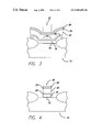
- FIG. 3 is a cross-section through the partially fabricated memory device taken in a section perpendicular to the view illustrated in FIG. 2 .
- the process step illustrated is known as the “stack etch” because of the stacked nature of the several layers in the resulting structure.
- the previously applied photoresist layer 28 is removed and an additional layer of photoresist is applied and patterned to form patterned photoresist region 32 overlying the anti-reflective coating film.
- the objective in this process step is to etch through both polycrystalline silicon layers 22 and 18 , interpoly dielectric layer 20 and gate oxide layer 16 to form a stacked structure bounded by the dashed lines 34 .
- the etching is accomplished by reactive ion etching or other directional etching as is well known in the art.
- the ARC film aids in replicating the pattern from a mask (not shown) in the photoresist layer 32
- the use of the ARC film reduces reflections from, for example, any underlying steps in the topography. Such steps may be especially severe at this stage of the device processing because the steps now also include those steps found at the edge of polycrystalline silicon layer 22 as previously patterned.
- FIG. 4 illustrates a stacked structure which results from the etching described above and the subsequent removal of patterned photoresist portion 32 .
- the stacked structure includes a first gate oxide 16 , floating gate 18 , interpoly dielectric 20 and control gate 22 .
- the stacked structure is precisely aligned with respect to the active area with each of the layers of the structure aligned to the layers above and below.
- the stacked structure at this point in the process, also includes layers 24 and 26 of the anti-reflective coating film. It remains to remove the anti-reflective coating from the top of the stack so that the processing can continue.
- Removal of the silicon oxynitride layer 26 must be accomplished without serious etching of the edges of any of the layers of the stack structure, and especially without any serious etching of the exposed edge of the silicon nitride included in the interpoly dielectric.
- Plasma etching of the silicon oxynitride layer 26 has proved unsuccessful because high etch selectivity of silicon oxynitride to exposed silicon is very difficult to achieve.
- Hot phosphoric acid is well known as an etchant for silicon nitride. It has been discovered, in accordance with the invention, that the as-deposited silicon oxynitride also can be etched in hot phosphoric acid provided that the silicon oxynitride has not been exposed to any temperatures in excess of about 400° C. prior to the etching step. If the stack structure 36 has been re-oxidized after the polycrystalline silicon etch, as is a routine process in many MOS process technologies, the etch rate of the silicon oxynitride in hot phosphoric acid is only about 0.2 nm per minute.
- etching of the silicon oxynitride film 26 prior to any high temperature heat treatment results in an etch rate in the hot phosphoric acid of about 6 nm per minute.
- silicon oxynitride layer 26 can be totally removed without deleteriously etching the exposed edge of the silicon nitride.
- the hot phosphoric acid etching of silicon oxynitride is carried out with the same etch composition and etch conditions as is the well know etching of silicon nitride.
- FIG. 5 illustrates, in cross-section, the resulting stack structure after removal of the silicon oxynitride layer 26 in hot phosphoric acid.
- the slight etching of the exposed edge of the nitride layer included in the interpoly dielectric layer is noted by the notch 40 .
- the thin oxide layer 24 is also shown to have been removed in this view. Oxide layer 24 is easily removed in known manner.
- FIG. 6 illustrates, in cross-section, the stack structure 36 after the exposed edges of polycrystalline silicon layer 22 and floating gate 18 have been reoxidized.
- the reoxidation is accomplished by placing the structure in an oxidizing ambient at an elevated temperature for a sufficient time to grow oxide layer 42 on polycrystalline silicon layer 22 and oxide layer 44 on floating gate 18 .
- Oxide layers 42 and 44 are grown to a thickness of about 10 nm so that the edges of the floating gate 18 and the control gate 22 are again brought into alignment with the edge of the silicon nitride layer that was etched during the removal of the anti-reflective coating film.
- FIG. 7 illustrates, in cross-section, an alternate embodiment of the invention.
- a layer of oxide is deposited by low temperature chemical vapor deposition to cover all exposed surfaces of the device.
- This oxide layer can be deposited, in known manner, for example by plasma enhanced CVD from a TEOS source, at a temperature of less than 400° C.
- the deposited oxide layer is then exposed to a reactive ion etch which selectively removes the oxide from exposed horizontal surfaces while leaving a sidewall oxide 50 on vertical surfaces.
- the process of reactive ion etching or other directional etching to leave sidewall oxide 50 is well known in the art.
- Sidewall oxide 50 serves to protect the previously exposed edge of the nitride layer included in interpoly dielectric layer 20 .
- the silicon oxynitride layer 26 can then be etched, in accordance with the invention, in hot phosphoric acid without etching the interpoly dielectric layer.
- the oxide to form sidewall oxide 50 at a temperature of less than about 400° C., the rapid etchability of silicon oxynitride layer 26 in hot phosphoric acid is maintained.
- the processing of the structure illustrated in either FIG. 6 or FIG. 7 can then continue, in known manner, to complete the semiconductor device structure.
- the remaining steps include, for example, the formation of diffused or otherwise doped regions in substrate 12 , the provision of contacts and interconnections, and the like.
Abstract
Description
Claims (21)
Priority Applications (1)
| Application Number | Priority Date | Filing Date | Title |
|---|---|---|---|
| US09/370,508 US6924196B1 (en) | 1999-08-06 | 1999-08-06 | Anti-reflective coating and process using an anti-reflective coating |
Applications Claiming Priority (1)
| Application Number | Priority Date | Filing Date | Title |
|---|---|---|---|
| US09/370,508 US6924196B1 (en) | 1999-08-06 | 1999-08-06 | Anti-reflective coating and process using an anti-reflective coating |
Publications (1)
| Publication Number | Publication Date |
|---|---|
| US6924196B1 true US6924196B1 (en) | 2005-08-02 |
Family
ID=34794137
Family Applications (1)
| Application Number | Title | Priority Date | Filing Date |
|---|---|---|---|
| US09/370,508 Expired - Lifetime US6924196B1 (en) | 1999-08-06 | 1999-08-06 | Anti-reflective coating and process using an anti-reflective coating |
Country Status (1)
| Country | Link |
|---|---|
| US (1) | US6924196B1 (en) |
Cited By (5)
| Publication number | Priority date | Publication date | Assignee | Title |
|---|---|---|---|---|
| US20040121146A1 (en) * | 2002-12-20 | 2004-06-24 | Xiao-Ming He | Composite barrier films and method |
| US7026213B1 (en) * | 2005-04-22 | 2006-04-11 | Hynix Semiconductor Inc. | Method of fabricating flash memory device |
| DE102009012546A1 (en) | 2009-03-10 | 2010-09-23 | X-Fab Semiconductor Foundries Ag | Mono anti-reflection silicon nitride layer for use on switching circuits with e.g. photodiodes, by single-step plasma enhanced chemical vapor deposition method, is designed as protective layer against data degradation of elements |
| US20110151222A1 (en) * | 2009-12-22 | 2011-06-23 | Agc Flat Glass North America, Inc. | Anti-reflective coatings and methods of making the same |
| US20190371396A1 (en) * | 2008-12-19 | 2019-12-05 | Unity Semiconductor Corporation | Conductive metal oxide structures in non-volatile re-writable memory devices |
Citations (6)
| Publication number | Priority date | Publication date | Assignee | Title |
|---|---|---|---|---|
| US5597754A (en) * | 1995-05-25 | 1997-01-28 | Industrial Technology Research Institute | Increased surface area for DRAM, storage node capacitors, using a novel polysilicon deposition and anneal process |
| US5605601A (en) * | 1995-09-19 | 1997-02-25 | Mitsubishi Denki Kabushiki Kaisha | Method of manufacturing semiconductor device |
| US5620913A (en) * | 1996-05-28 | 1997-04-15 | Chartered Semiconductor Manufacturing Pte Ltd. | Method of making a flash memory cell |
| US5968324A (en) * | 1995-12-05 | 1999-10-19 | Applied Materials, Inc. | Method and apparatus for depositing antireflective coating |
| US6030541A (en) * | 1998-06-19 | 2000-02-29 | International Business Machines Corporation | Process for defining a pattern using an anti-reflective coating and structure therefor |
| US6245682B1 (en) * | 1999-03-11 | 2001-06-12 | Taiwan Semiconductor Manufacturing Company | Removal of SiON ARC film after poly photo and etch |
-
1999
- 1999-08-06 US US09/370,508 patent/US6924196B1/en not_active Expired - Lifetime
Patent Citations (6)
| Publication number | Priority date | Publication date | Assignee | Title |
|---|---|---|---|---|
| US5597754A (en) * | 1995-05-25 | 1997-01-28 | Industrial Technology Research Institute | Increased surface area for DRAM, storage node capacitors, using a novel polysilicon deposition and anneal process |
| US5605601A (en) * | 1995-09-19 | 1997-02-25 | Mitsubishi Denki Kabushiki Kaisha | Method of manufacturing semiconductor device |
| US5968324A (en) * | 1995-12-05 | 1999-10-19 | Applied Materials, Inc. | Method and apparatus for depositing antireflective coating |
| US5620913A (en) * | 1996-05-28 | 1997-04-15 | Chartered Semiconductor Manufacturing Pte Ltd. | Method of making a flash memory cell |
| US6030541A (en) * | 1998-06-19 | 2000-02-29 | International Business Machines Corporation | Process for defining a pattern using an anti-reflective coating and structure therefor |
| US6245682B1 (en) * | 1999-03-11 | 2001-06-12 | Taiwan Semiconductor Manufacturing Company | Removal of SiON ARC film after poly photo and etch |
Non-Patent Citations (2)
| Title |
|---|
| Wolf et al., Silicon Processing for the VLSI Era, 1986, vol. 1, p. 539-542. * |
| Wolf et al; Silicon Processing for the VLSI Era; vol. 1; 1986; p. 5 429-455, 518. * |
Cited By (7)
| Publication number | Priority date | Publication date | Assignee | Title |
|---|---|---|---|---|
| US20040121146A1 (en) * | 2002-12-20 | 2004-06-24 | Xiao-Ming He | Composite barrier films and method |
| US20050109606A1 (en) * | 2002-12-20 | 2005-05-26 | Xiao-Ming He | Composite barrier films and method |
| US7026213B1 (en) * | 2005-04-22 | 2006-04-11 | Hynix Semiconductor Inc. | Method of fabricating flash memory device |
| US20190371396A1 (en) * | 2008-12-19 | 2019-12-05 | Unity Semiconductor Corporation | Conductive metal oxide structures in non-volatile re-writable memory devices |
| US10803935B2 (en) * | 2008-12-19 | 2020-10-13 | Unity Semiconductor Corporation | Conductive metal oxide structures in non-volatile re-writable memory devices |
| DE102009012546A1 (en) | 2009-03-10 | 2010-09-23 | X-Fab Semiconductor Foundries Ag | Mono anti-reflection silicon nitride layer for use on switching circuits with e.g. photodiodes, by single-step plasma enhanced chemical vapor deposition method, is designed as protective layer against data degradation of elements |
| US20110151222A1 (en) * | 2009-12-22 | 2011-06-23 | Agc Flat Glass North America, Inc. | Anti-reflective coatings and methods of making the same |
Similar Documents
| Publication | Publication Date | Title |
|---|---|---|
| US6794230B2 (en) | Approach to improve line end shortening | |
| US5604157A (en) | Reduced notching of polycide gates using silicon anti reflection layer | |
| JPH08255752A (en) | Semiconductor element with low reflectance coating and its preparation | |
| WO2005122254A2 (en) | Gate stack and gate stack etch sequence for metal gate integration | |
| US5643833A (en) | Method of making a contact hole in a semiconductor device | |
| US6395644B1 (en) | Process for fabricating a semiconductor device using a silicon-rich silicon nitride ARC | |
| KR100225327B1 (en) | Semiconductor device having a polycide structure and method of manufacturing the same | |
| JPH10163107A (en) | (ge, si)nx reflection prevention film and pattern formation method using it | |
| US6255717B1 (en) | Shallow trench isolation using antireflection layer | |
| KR100268894B1 (en) | Method for forming of flash memory device | |
| US6187687B1 (en) | Minimization of line width variation in photolithography | |
| US6924196B1 (en) | Anti-reflective coating and process using an anti-reflective coating | |
| US20050118531A1 (en) | Method for controlling critical dimension by utilizing resist sidewall protection | |
| KR100219550B1 (en) | Anti-reflective coating layer and pattern forming method using the same | |
| US6420095B1 (en) | Manufacture of semiconductor device using A-C anti-reflection coating | |
| US5871886A (en) | Sandwiched middle antireflection coating (SMARC) process | |
| JP3700231B2 (en) | Method for forming connection hole | |
| JP2002110654A (en) | Method of manufacturing semiconductor device | |
| US6184116B1 (en) | Method to fabricate the MOS gate | |
| US6074905A (en) | Formation of a thin oxide protection layer at poly sidewall and area surface | |
| US6703297B1 (en) | Method of removing inorganic gate antireflective coating after spacer formation | |
| JPH0846188A (en) | Semiconductor device | |
| US6200886B1 (en) | Fabricating process for polysilicon gate | |
| US7097921B2 (en) | Sandwich arc structure for preventing metal to contact from shifting | |
| KR100910865B1 (en) | Method for fabrication of semiconductor device |
Legal Events
| Date | Code | Title | Description |
|---|---|---|---|
| AS | Assignment |
Owner name: CONEXANT SYSTEMS, INC., CALIFORNIA Free format text: ASSIGNMENT OF ASSIGNORS INTEREST;ASSIGNORS:SHARMA, UMESH;YIN, KEVIN Q.;WU, HONG J.;AND OTHERS;REEL/FRAME:010157/0981 Effective date: 19990726 |
|
| AS | Assignment |
Owner name: CREDIT SUISSE FIRST BOSTON, NEW YORK Free format text: SECURITY INTEREST;ASSIGNOR:CONEXANT SYSTEMS, INC.;REEL/FRAME:010450/0899 Effective date: 19981221 |
|
| AS | Assignment |
Owner name: BROOKTREE CORPORATION, CALIFORNIA Free format text: RELEASE OF SECURITY INTEREST;ASSIGNOR:CREDIT SUISSE FIRST BOSTON;REEL/FRAME:012252/0865 Effective date: 20011018 Owner name: CONEXANT SYSTEMS, INC., CALIFORNIA Free format text: RELEASE OF SECURITY INTEREST;ASSIGNOR:CREDIT SUISSE FIRST BOSTON;REEL/FRAME:012252/0865 Effective date: 20011018 Owner name: CONEXANT SYSTEMS WORLDWIDE, INC., CALIFORNIA Free format text: RELEASE OF SECURITY INTEREST;ASSIGNOR:CREDIT SUISSE FIRST BOSTON;REEL/FRAME:012252/0865 Effective date: 20011018 Owner name: BROOKTREE WORLDWIDE SALES CORPORATION, CALIFORNIA Free format text: RELEASE OF SECURITY INTEREST;ASSIGNOR:CREDIT SUISSE FIRST BOSTON;REEL/FRAME:012252/0865 Effective date: 20011018 |
|
| AS | Assignment |
Owner name: NEWPORT FAB, LLC, CALIFORNIA Free format text: ASSIGNMENT OF ASSIGNORS INTEREST;ASSIGNOR:CONEXANT SYSTEMS, INC.;REEL/FRAME:012754/0852 Effective date: 20020312 |
|
| AS | Assignment |
Owner name: NEWPORT FAB, LLC, CALIFORNIA Free format text: ASSIGNMENT OF ASSIGNORS INTEREST;ASSIGNOR:CONEXANT SYSTEMS, INC.;REEL/FRAME:013280/0690 Effective date: 20020312 |
|
| STCF | Information on status: patent grant |
Free format text: PATENTED CASE |
|
| AS | Assignment |
Owner name: WACHOVIA CAPITAL FINANCE CORPORATION (WESTERN), CA Free format text: SECURITY AGREEMENT;ASSIGNOR:NEWPORT FAB, LLC;REEL/FRAME:017223/0083 Effective date: 20060106 |
|
| AS | Assignment |
Owner name: WACHOVIA CAPITAL FINANCE CORPORATION (WESTERN), CA Free format text: SECURITY AGREEMENT;ASSIGNOR:NEWPORT FAB, LLC;REEL/FRAME:017586/0081 Effective date: 20060106 |
|
| FPAY | Fee payment |
Year of fee payment: 4 |
|
| FPAY | Fee payment |
Year of fee payment: 8 |
|
| FPAY | Fee payment |
Year of fee payment: 12 |
|
| AS | Assignment |
Owner name: NEWPORT FAB, LLC DBA JAZZ SEMICONDUCTOR OPERATING COMPANY, CALIFORNIA Free format text: RELEASE BY SECURED PARTY;ASSIGNOR:WELLS FARGO CAPITAL FINANCE, LLC, AS SUCCESSOR BY MERGER TO WACHOVIA CAPITAL FINANCE CORPORATION (WESTERN);REEL/FRAME:065284/0123 Effective date: 20230929 |