US6897284B2 - Polythiophenes and devices thereof - Google Patents
Polythiophenes and devices thereof Download PDFInfo
- Publication number
- US6897284B2 US6897284B2 US10/392,592 US39259203A US6897284B2 US 6897284 B2 US6897284 B2 US 6897284B2 US 39259203 A US39259203 A US 39259203A US 6897284 B2 US6897284 B2 US 6897284B2
- Authority
- US
- United States
- Prior art keywords
- accordance
- polythiophene
- thin film
- film transistor
- alkyl
- Prior art date
- Legal status (The legal status is an assumption and is not a legal conclusion. Google has not performed a legal analysis and makes no representation as to the accuracy of the status listed.)
- Expired - Lifetime, expires
Links
- 0 *C1=C(C)SC(C)=C1.BC1=C(C)SC(C)=C1.C[2H]C Chemical compound *C1=C(C)SC(C)=C1.BC1=C(C)SC(C)=C1.C[2H]C 0.000 description 11
- UUHIWOVRTTZXHR-UHFFFAOYSA-N C.C.C.C#CC#CC#CC#COC1=C(C2=CC=C(C)S2)C=C(OCCCCCCCC)C(C2=CC=C(C)S2)=C1.C#CC#CC#CC#COC1=C(C2=CC=C(C3=C(CCCCCCCC)C=C(C)S3)S2)C=C(OCCCCCCCC)C(C2=CC=C(C3=C(CCCCCCCC)C=C(C)S3)S2)=C1.CCCCCCC1=C(C2=CC=C(C3=C(CCCCCC)C=C(C)S3)S2)SC(C)=C1.CCCCCCCCC1=C(C2=CC=C(C)S2)SC(C2=CC=C(C)S2)=C1CCCCCCCC.CCCCCCCCCCC1=C(C2=CC=C(C3=CC=C(C4=C(CCCCCCCCCC)C=C(C)S4)S3)S2)SC(C)=C1.CCCCCCCCCCCCC1=C(C2=CC=C(C)S2)SC(C2=CC=C(C)S2)=C1CCCCCCCCCCCC.CCCCCCCCCCCCC1=C(C2=CC=C(C3=CC=C(C4=C(CCCCCCCCCCCC)C=C(C)S4)S3)S2)SC(C)=C1.CCCCCCCCCCCCC1=C(C2=CC=C(C3=CC=C(C4=CC=C(C5=C(CCCCCCCCCCCC)C=C(C)S5)S4)S3)S2)SC(C)=C1.[HH].[HH].[HH].[HH].[HH].[HH].[HH].[HH].[HH].[HH].[HH].[HH].[HH].[HH].[HH].[HH] Chemical compound C.C.C.C#CC#CC#CC#COC1=C(C2=CC=C(C)S2)C=C(OCCCCCCCC)C(C2=CC=C(C)S2)=C1.C#CC#CC#CC#COC1=C(C2=CC=C(C3=C(CCCCCCCC)C=C(C)S3)S2)C=C(OCCCCCCCC)C(C2=CC=C(C3=C(CCCCCCCC)C=C(C)S3)S2)=C1.CCCCCCC1=C(C2=CC=C(C3=C(CCCCCC)C=C(C)S3)S2)SC(C)=C1.CCCCCCCCC1=C(C2=CC=C(C)S2)SC(C2=CC=C(C)S2)=C1CCCCCCCC.CCCCCCCCCCC1=C(C2=CC=C(C3=CC=C(C4=C(CCCCCCCCCC)C=C(C)S4)S3)S2)SC(C)=C1.CCCCCCCCCCCCC1=C(C2=CC=C(C)S2)SC(C2=CC=C(C)S2)=C1CCCCCCCCCCCC.CCCCCCCCCCCCC1=C(C2=CC=C(C3=CC=C(C4=C(CCCCCCCCCCCC)C=C(C)S4)S3)S2)SC(C)=C1.CCCCCCCCCCCCC1=C(C2=CC=C(C3=CC=C(C4=CC=C(C5=C(CCCCCCCCCCCC)C=C(C)S5)S4)S3)S2)SC(C)=C1.[HH].[HH].[HH].[HH].[HH].[HH].[HH].[HH].[HH].[HH].[HH].[HH].[HH].[HH].[HH].[HH] UUHIWOVRTTZXHR-UHFFFAOYSA-N 0.000 description 2
- XAHQFJMLIWWJDM-UHFFFAOYSA-N CC1=C2OCCOC2=C(C)S1.CCCCCCCCC1(CCCCCCCC)COC2=C(C)SC(C)=C2OC1.COCCOCCOCCOC1=C(C)SC(C)=C1.COCCOCCOCCOC1=C(C)SC(C)=C1C Chemical compound CC1=C2OCCOC2=C(C)S1.CCCCCCCCC1(CCCCCCCC)COC2=C(C)SC(C)=C2OC1.COCCOCCOCCOC1=C(C)SC(C)=C1.COCCOCCOCCOC1=C(C)SC(C)=C1C XAHQFJMLIWWJDM-UHFFFAOYSA-N 0.000 description 2
- KUUYGVCERSNFDH-UHFFFAOYSA-N C#CC#CC#CC#CC#CC#CC1=C(C2=CC=C(C3=CC=C(C4=C(CCCCCCCCCCCC)C=C(C)S4)S3)S2)SC(C)=C1.C#CC#CC#CC#COC1=C(C2=CC=C(C)S2)C=C(OCCCCCCCC)C(C2=CC=C(C)S2)=C1.C#CC#CC#CC#COC1=C(C2=CC=C(C3=CC(CCCCCCCC)=C(C4=CC=C(C5=C(CCCCCCCC)C=C(C)S5)S4)C=C3OCCCCCCCC)S2)SC(C)=C1.CCCCCCC1=C(C)SC(C)=C1.CCCCCCC1=C(C2=CC=C(C3=C(CCCCCC)C=C(C)S3)S2)SC(C)=C1.CCCCCCCCC1=C(C)SC(C)=C1.CCCCCCCCC1=C(C2=CC=C(C)S2)SC(C2=CC=C(C)S2)=C1CCCCCCCC.CCCCCCCCCCC1=C(C2=CC=C(C3=CC=C(C4=C(CCCCCCCCCC)C=C(C)S4)S3)S2)SC(C)=C1.CCCCCCCCCCCCC1=C(C2=CC=C(C)S2)SC(C2=CC=C(C)S2)=C1CCCCCCCCCCCC.CCCCCCCCCCCCC1=C(C2=CC=C(C3=CC=C(C4=CC=C(C5=C(CCCCCCCCCCCC)C=C(C)S5)S4)S3)S2)SC(C)=C1.[HH].[HH].[HH].[HH].[HH].[HH].[HH].[HH].[HH].[HH].[HH].[HH].[HH].[HH].[HH].[HH].[HH].[HH].[HH].[HH].[HH].[HH].[HH].[HH].[HH].[HH] Chemical compound C#CC#CC#CC#CC#CC#CC1=C(C2=CC=C(C3=CC=C(C4=C(CCCCCCCCCCCC)C=C(C)S4)S3)S2)SC(C)=C1.C#CC#CC#CC#COC1=C(C2=CC=C(C)S2)C=C(OCCCCCCCC)C(C2=CC=C(C)S2)=C1.C#CC#CC#CC#COC1=C(C2=CC=C(C3=CC(CCCCCCCC)=C(C4=CC=C(C5=C(CCCCCCCC)C=C(C)S5)S4)C=C3OCCCCCCCC)S2)SC(C)=C1.CCCCCCC1=C(C)SC(C)=C1.CCCCCCC1=C(C2=CC=C(C3=C(CCCCCC)C=C(C)S3)S2)SC(C)=C1.CCCCCCCCC1=C(C)SC(C)=C1.CCCCCCCCC1=C(C2=CC=C(C)S2)SC(C2=CC=C(C)S2)=C1CCCCCCCC.CCCCCCCCCCC1=C(C2=CC=C(C3=CC=C(C4=C(CCCCCCCCCC)C=C(C)S4)S3)S2)SC(C)=C1.CCCCCCCCCCCCC1=C(C2=CC=C(C)S2)SC(C2=CC=C(C)S2)=C1CCCCCCCCCCCC.CCCCCCCCCCCCC1=C(C2=CC=C(C3=CC=C(C4=CC=C(C5=C(CCCCCCCCCCCC)C=C(C)S5)S4)S3)S2)SC(C)=C1.[HH].[HH].[HH].[HH].[HH].[HH].[HH].[HH].[HH].[HH].[HH].[HH].[HH].[HH].[HH].[HH].[HH].[HH].[HH].[HH].[HH].[HH].[HH].[HH].[HH].[HH] KUUYGVCERSNFDH-UHFFFAOYSA-N 0.000 description 1
- AUXHBGDHKOQDCY-UHFFFAOYSA-N C#CC#CC#CC#CC#COC1=C(C2=CC=C(C3=C(C)C=C(C)S3)S2)C=C(OCCCCCCCCCC)C(C2=CC=C(C3=C(C)C=C(C)S3)S2)=C1.CCCCCCC1=C(C2=CC(CCCCCC)=C(C3=CC=C(C4=CC=C(C5=C(CCCCCC)C=C(C6=C(CCCCCC)C=C(C)S6)S5)S4)S3)S2)SC(C)=C1.CCCCCCCCC1=CC(C2=CC=C(C)S2)=C(CCCCCCCC)C=C1C1=CC=C(C)S1.CCCCCCCCC1=CC(C2=CC=C(C3=C(CCCCCCCC)C=C(C)S3)S2)=C(CCCCCCCC)C=C1C1=CC=C(C2=C(CCCCCCCC)C=C(C)S2)S1.CCCCCCCCCCC1=C(C2=CC=C(C3=C(CCCCCCCCCC)C=C(C4=CC=C(C)S4)S3)S2)SC(C)=C1.CCCCCCCCCCCCC1=C(C2=CC=C(C3=CC=C(C4=C(CCCCCCCCCCCC)C=C(C5=CC=C(C6=CC=C(C)S6)S5)S4)S3)S2)SC(C)=C1.COCCOCCOCC1=C(C2=CC=C(C3=CC=C(C4=C(COCCOCCOC)C=C(C)S4)S3)S2)SC(C)=C1.COCCOCCOCCOC1=C(C)SC(C)=C1.COCCOCCOCCOC1=C(C)SC(C)=C1C.[HH].[HH].[HH].[HH].[HH].[HH].[HH].[HH].[HH].[HH] Chemical compound C#CC#CC#CC#CC#COC1=C(C2=CC=C(C3=C(C)C=C(C)S3)S2)C=C(OCCCCCCCCCC)C(C2=CC=C(C3=C(C)C=C(C)S3)S2)=C1.CCCCCCC1=C(C2=CC(CCCCCC)=C(C3=CC=C(C4=CC=C(C5=C(CCCCCC)C=C(C6=C(CCCCCC)C=C(C)S6)S5)S4)S3)S2)SC(C)=C1.CCCCCCCCC1=CC(C2=CC=C(C)S2)=C(CCCCCCCC)C=C1C1=CC=C(C)S1.CCCCCCCCC1=CC(C2=CC=C(C3=C(CCCCCCCC)C=C(C)S3)S2)=C(CCCCCCCC)C=C1C1=CC=C(C2=C(CCCCCCCC)C=C(C)S2)S1.CCCCCCCCCCC1=C(C2=CC=C(C3=C(CCCCCCCCCC)C=C(C4=CC=C(C)S4)S3)S2)SC(C)=C1.CCCCCCCCCCCCC1=C(C2=CC=C(C3=CC=C(C4=C(CCCCCCCCCCCC)C=C(C5=CC=C(C6=CC=C(C)S6)S5)S4)S3)S2)SC(C)=C1.COCCOCCOCC1=C(C2=CC=C(C3=CC=C(C4=C(COCCOCCOC)C=C(C)S4)S3)S2)SC(C)=C1.COCCOCCOCCOC1=C(C)SC(C)=C1.COCCOCCOCCOC1=C(C)SC(C)=C1C.[HH].[HH].[HH].[HH].[HH].[HH].[HH].[HH].[HH].[HH] AUXHBGDHKOQDCY-UHFFFAOYSA-N 0.000 description 1
- JGOUDVJECJNEOY-UHFFFAOYSA-N C#CC#CC#CC#CC#COC1=C(C2=CC=C(C3=C(C)C=C(C)S3)S2)C=C(OCCCCCCCCCC)C(C2=CC=C(C3=C(C)C=C(C)S3)S2)=C1.CCCCCCCCC1=CC(C2=CC=C(C)S2)=C(CCCCCCCC)C=C1C1=CC=C(C)S1.[HH].[HH].[HH].[HH].[HH].[HH].[HH].[HH].[HH].[HH] Chemical compound C#CC#CC#CC#CC#COC1=C(C2=CC=C(C3=C(C)C=C(C)S3)S2)C=C(OCCCCCCCCCC)C(C2=CC=C(C3=C(C)C=C(C)S3)S2)=C1.CCCCCCCCC1=CC(C2=CC=C(C)S2)=C(CCCCCCCC)C=C1C1=CC=C(C)S1.[HH].[HH].[HH].[HH].[HH].[HH].[HH].[HH].[HH].[HH] JGOUDVJECJNEOY-UHFFFAOYSA-N 0.000 description 1
- XBRPTWJKJNZQIN-UHFFFAOYSA-N C#CC#CC#CC#COC1=C(C2=CC=C(C)S2)C=C(OCCCCCCCC)C(C2=CC=C(C)S2)=C1.C#CC#CC#CC#COC1=C(C2=CC=C(C3=C(CCCCCCCC)C=C(C)S3)S2)C=C(OCCCCCCCC)C(C2=CC=C(C3=C(CCCCCCCC)C=C(C)S3)S2)=C1.CCCCCCC1=C(C2=CC=C(C3=C(CCCCCC)C=C(C)S3)S2)SC(C)=C1.CCCCCCCCC1=C(C2=CC=C(C)S2)SC(C2=CC=C(C)S2)=C1CCCCCCCC.CCCCCCCCCCC1=C(C2=CC=C(C3=CC=C(C4=C(CCCCCCCCCC)C=C(C)S4)S3)S2)SC(C)=C1.CCCCCCCCCCCCC1=C(C2=CC=C(C)S2)SC(C2=CC=C(C)S2)=C1CCCCCCCCCCCC.CCCCCCCCCCCCC1=C(C2=CC=C(C3=CC=C(C4=C(CCCCCCCCCCCC)C=C(C)S4)S3)S2)SC(C)=C1.CCCCCCCCCCCCC1=C(C2=CC=C(C3=CC=C(C4=CC=C(C5=C(CCCCCCCCCCCC)C=C(C)S5)S4)S3)S2)SC(C)=C1.[HH].[HH].[HH].[HH].[HH].[HH].[HH].[HH].[HH].[HH].[HH].[HH].[HH].[HH].[HH].[HH] Chemical compound C#CC#CC#CC#COC1=C(C2=CC=C(C)S2)C=C(OCCCCCCCC)C(C2=CC=C(C)S2)=C1.C#CC#CC#CC#COC1=C(C2=CC=C(C3=C(CCCCCCCC)C=C(C)S3)S2)C=C(OCCCCCCCC)C(C2=CC=C(C3=C(CCCCCCCC)C=C(C)S3)S2)=C1.CCCCCCC1=C(C2=CC=C(C3=C(CCCCCC)C=C(C)S3)S2)SC(C)=C1.CCCCCCCCC1=C(C2=CC=C(C)S2)SC(C2=CC=C(C)S2)=C1CCCCCCCC.CCCCCCCCCCC1=C(C2=CC=C(C3=CC=C(C4=C(CCCCCCCCCC)C=C(C)S4)S3)S2)SC(C)=C1.CCCCCCCCCCCCC1=C(C2=CC=C(C)S2)SC(C2=CC=C(C)S2)=C1CCCCCCCCCCCC.CCCCCCCCCCCCC1=C(C2=CC=C(C3=CC=C(C4=C(CCCCCCCCCCCC)C=C(C)S4)S3)S2)SC(C)=C1.CCCCCCCCCCCCC1=C(C2=CC=C(C3=CC=C(C4=CC=C(C5=C(CCCCCCCCCCCC)C=C(C)S5)S4)S3)S2)SC(C)=C1.[HH].[HH].[HH].[HH].[HH].[HH].[HH].[HH].[HH].[HH].[HH].[HH].[HH].[HH].[HH].[HH] XBRPTWJKJNZQIN-UHFFFAOYSA-N 0.000 description 1
- MKCFFWNKZCFZBM-UHFFFAOYSA-N C.C.C.C#CC#CC#CC#COC1=C(C2=CC=C(C)S2)C=C(OCCCCCCCC)C(C2=CC=C(C)S2)=C1.CCCCCCC1=C(C)SC(C)=C1.CCCCCCC1=C(C2=CC=C(C3=C(CCCCCC)C=C(C)S3)S2)SC(C)=C1.CCCCCCCCC1=C(C)SC(C)=C1.CCCCCCCCC1=C(C2=CC=C(C)S2)SC(C2=CC=C(C)S2)=C1CCCCCCCC.CCCCCCCCCCC1=C(C2=CC=C(C3=CC=C(C4=C(CCCCCCCCCC)C=C(C)S4)S3)S2)SC(C)=C1.CCCCCCCCCCCCC1=C(C2=CC=C(C)S2)SC(C2=CC=C(C)S2)=C1CCCCCCCCCCCC.CCCCCCCCCCCCC1=C(C2=CC=C(C3=CC=C(C4=C(CCCCCCCCCCCC)C=C(C)S4)S3)S2)SC(C)=C1.CCCCCCCCCCCCC1=C(C2=CC=C(C3=CC=C(C4=CC=C(C5=C(CCCCCCCCCCCC)C=C(C)S5)S4)S3)S2)SC(C)=C1.[HH].[HH].[HH].[HH].[HH].[HH].[HH].[HH] Chemical compound C.C.C.C#CC#CC#CC#COC1=C(C2=CC=C(C)S2)C=C(OCCCCCCCC)C(C2=CC=C(C)S2)=C1.CCCCCCC1=C(C)SC(C)=C1.CCCCCCC1=C(C2=CC=C(C3=C(CCCCCC)C=C(C)S3)S2)SC(C)=C1.CCCCCCCCC1=C(C)SC(C)=C1.CCCCCCCCC1=C(C2=CC=C(C)S2)SC(C2=CC=C(C)S2)=C1CCCCCCCC.CCCCCCCCCCC1=C(C2=CC=C(C3=CC=C(C4=C(CCCCCCCCCC)C=C(C)S4)S3)S2)SC(C)=C1.CCCCCCCCCCCCC1=C(C2=CC=C(C)S2)SC(C2=CC=C(C)S2)=C1CCCCCCCCCCCC.CCCCCCCCCCCCC1=C(C2=CC=C(C3=CC=C(C4=C(CCCCCCCCCCCC)C=C(C)S4)S3)S2)SC(C)=C1.CCCCCCCCCCCCC1=C(C2=CC=C(C3=CC=C(C4=CC=C(C5=C(CCCCCCCCCCCC)C=C(C)S5)S4)S3)S2)SC(C)=C1.[HH].[HH].[HH].[HH].[HH].[HH].[HH].[HH] MKCFFWNKZCFZBM-UHFFFAOYSA-N 0.000 description 1
- UPHQEGCGAWSOKB-UHFFFAOYSA-N C.C.C.C#CC#CC#CC#COC1=C(C2=CC=C(C)S2)C=C(OCCCCCCCC)C(C2=CC=C(C)S2)=C1.CCCCCCC1=C(C)SC(C)=C1.CCCCCCC1=C(C2=CC=C(C3=C(CCCCCC)C=C(C)S3)S2)SC(C)=C1.CCCCCCCCC1=C(C)SC(C)=C1.CCCCCCCCCCC1=C(C2=CC=C(C3=CC=C(C4=C(CCCCCCCCCC)C=C(C)S4)S3)S2)SC(C)=C1.CCCCCCCCCCCCC1=C(C2=CC=C(C3=CC=C(C4=C(CCCCCCCCCCCC)C=C(C)S4)S3)S2)SC(C)=C1.CCCCCCCCCCCCC1=C(C2=CC=C(C3=CC=C(C4=CC=C(C5=C(CCCCCCCCCCCC)C=C(C)S5)S4)S3)S2)SC(C)=C1.[HH].[HH].[HH].[HH].[HH].[HH].[HH].[HH] Chemical compound C.C.C.C#CC#CC#CC#COC1=C(C2=CC=C(C)S2)C=C(OCCCCCCCC)C(C2=CC=C(C)S2)=C1.CCCCCCC1=C(C)SC(C)=C1.CCCCCCC1=C(C2=CC=C(C3=C(CCCCCC)C=C(C)S3)S2)SC(C)=C1.CCCCCCCCC1=C(C)SC(C)=C1.CCCCCCCCCCC1=C(C2=CC=C(C3=CC=C(C4=C(CCCCCCCCCC)C=C(C)S4)S3)S2)SC(C)=C1.CCCCCCCCCCCCC1=C(C2=CC=C(C3=CC=C(C4=C(CCCCCCCCCCCC)C=C(C)S4)S3)S2)SC(C)=C1.CCCCCCCCCCCCC1=C(C2=CC=C(C3=CC=C(C4=CC=C(C5=C(CCCCCCCCCCCC)C=C(C)S5)S4)S3)S2)SC(C)=C1.[HH].[HH].[HH].[HH].[HH].[HH].[HH].[HH] UPHQEGCGAWSOKB-UHFFFAOYSA-N 0.000 description 1
- NYVFLTUNAAMQKF-UHFFFAOYSA-J C.C.C.C.C1=CSC(CC2=CC=CS2)=C1.CC.CC.CC1=CC=C(CC2=CC=C(C)S2)S1.C[RaH].C[RaH].Cl[Fe](Cl)Cl.I[IH]I.[V]I Chemical compound C.C.C.C.C1=CSC(CC2=CC=CS2)=C1.CC.CC.CC1=CC=C(CC2=CC=C(C)S2)S1.C[RaH].C[RaH].Cl[Fe](Cl)Cl.I[IH]I.[V]I NYVFLTUNAAMQKF-UHFFFAOYSA-J 0.000 description 1
- KFAHEJKAESPCSV-UHFFFAOYSA-N C.C.CC1=CC=C(CC2=CC=C(C)S2)S1.C[RaH].C[Rb] Chemical compound C.C.CC1=CC=C(CC2=CC=C(C)S2)S1.C[RaH].C[Rb] KFAHEJKAESPCSV-UHFFFAOYSA-N 0.000 description 1
- ONOHVIQDRSQOGO-UHFFFAOYSA-N CC.CC1=CC=C(C2=CC(C)=C(C)S2)S1 Chemical compound CC.CC1=CC=C(C2=CC(C)=C(C)S2)S1 ONOHVIQDRSQOGO-UHFFFAOYSA-N 0.000 description 1
- XUECFOPTDRRCPZ-UHFFFAOYSA-N CC1=C2OCCOC2=C(C)S1.CCCCCCCCC1(CCCCCCCC)COC2=C(C)SC(C)=C2OC1 Chemical compound CC1=C2OCCOC2=C(C)S1.CCCCCCCCC1(CCCCCCCC)COC2=C(C)SC(C)=C2OC1 XUECFOPTDRRCPZ-UHFFFAOYSA-N 0.000 description 1
- QKZJQIHBRCFDGQ-UHFFFAOYSA-N CC1=CC(C)=C(C)S1 Chemical compound CC1=CC(C)=C(C)S1 QKZJQIHBRCFDGQ-UHFFFAOYSA-N 0.000 description 1
Images


Classifications
-
- C—CHEMISTRY; METALLURGY
- C08—ORGANIC MACROMOLECULAR COMPOUNDS; THEIR PREPARATION OR CHEMICAL WORKING-UP; COMPOSITIONS BASED THEREON
- C08G—MACROMOLECULAR COMPOUNDS OBTAINED OTHERWISE THAN BY REACTIONS ONLY INVOLVING UNSATURATED CARBON-TO-CARBON BONDS
- C08G61/00—Macromolecular compounds obtained by reactions forming a carbon-to-carbon link in the main chain of the macromolecule
- C08G61/12—Macromolecular compounds containing atoms other than carbon in the main chain of the macromolecule
- C08G61/122—Macromolecular compounds containing atoms other than carbon in the main chain of the macromolecule derived from five- or six-membered heterocyclic compounds, other than imides
- C08G61/123—Macromolecular compounds containing atoms other than carbon in the main chain of the macromolecule derived from five- or six-membered heterocyclic compounds, other than imides derived from five-membered heterocyclic compounds
- C08G61/126—Macromolecular compounds containing atoms other than carbon in the main chain of the macromolecule derived from five- or six-membered heterocyclic compounds, other than imides derived from five-membered heterocyclic compounds with a five-membered ring containing one sulfur atom in the ring
-
- H—ELECTRICITY
- H01—ELECTRIC ELEMENTS
- H01B—CABLES; CONDUCTORS; INSULATORS; SELECTION OF MATERIALS FOR THEIR CONDUCTIVE, INSULATING OR DIELECTRIC PROPERTIES
- H01B1/00—Conductors or conductive bodies characterised by the conductive materials; Selection of materials as conductors
- H01B1/06—Conductors or conductive bodies characterised by the conductive materials; Selection of materials as conductors mainly consisting of other non-metallic substances
- H01B1/12—Conductors or conductive bodies characterised by the conductive materials; Selection of materials as conductors mainly consisting of other non-metallic substances organic substances
- H01B1/124—Intrinsically conductive polymers
- H01B1/127—Intrinsically conductive polymers comprising five-membered aromatic rings in the main chain, e.g. polypyrroles, polythiophenes
-
- H—ELECTRICITY
- H10—SEMICONDUCTOR DEVICES; ELECTRIC SOLID-STATE DEVICES NOT OTHERWISE PROVIDED FOR
- H10K—ORGANIC ELECTRIC SOLID-STATE DEVICES
- H10K85/00—Organic materials used in the body or electrodes of devices covered by this subclass
- H10K85/10—Organic polymers or oligomers
- H10K85/111—Organic polymers or oligomers comprising aromatic, heteroaromatic, or aryl chains, e.g. polyaniline, polyphenylene or polyphenylene vinylene
- H10K85/113—Heteroaromatic compounds comprising sulfur or selene, e.g. polythiophene
-
- C—CHEMISTRY; METALLURGY
- C08—ORGANIC MACROMOLECULAR COMPOUNDS; THEIR PREPARATION OR CHEMICAL WORKING-UP; COMPOSITIONS BASED THEREON
- C08G—MACROMOLECULAR COMPOUNDS OBTAINED OTHERWISE THAN BY REACTIONS ONLY INVOLVING UNSATURATED CARBON-TO-CARBON BONDS
- C08G2261/00—Macromolecular compounds obtained by reactions forming a carbon-to-carbon link in the main chain of the macromolecule
- C08G2261/10—Definition of the polymer structure
- C08G2261/14—Side-groups
- C08G2261/142—Side-chains containing oxygen
- C08G2261/1424—Side-chains containing oxygen containing ether groups, including alkoxy
-
- C—CHEMISTRY; METALLURGY
- C08—ORGANIC MACROMOLECULAR COMPOUNDS; THEIR PREPARATION OR CHEMICAL WORKING-UP; COMPOSITIONS BASED THEREON
- C08G—MACROMOLECULAR COMPOUNDS OBTAINED OTHERWISE THAN BY REACTIONS ONLY INVOLVING UNSATURATED CARBON-TO-CARBON BONDS
- C08G2261/00—Macromolecular compounds obtained by reactions forming a carbon-to-carbon link in the main chain of the macromolecule
- C08G2261/30—Monomer units or repeat units incorporating structural elements in the main chain
- C08G2261/32—Monomer units or repeat units incorporating structural elements in the main chain incorporating heteroaromatic structural elements in the main chain
- C08G2261/322—Monomer units or repeat units incorporating structural elements in the main chain incorporating heteroaromatic structural elements in the main chain non-condensed
- C08G2261/3223—Monomer units or repeat units incorporating structural elements in the main chain incorporating heteroaromatic structural elements in the main chain non-condensed containing one or more sulfur atoms as the only heteroatom, e.g. thiophene
-
- H—ELECTRICITY
- H10—SEMICONDUCTOR DEVICES; ELECTRIC SOLID-STATE DEVICES NOT OTHERWISE PROVIDED FOR
- H10K—ORGANIC ELECTRIC SOLID-STATE DEVICES
- H10K10/00—Organic devices specially adapted for rectifying, amplifying, oscillating or switching; Organic capacitors or resistors having potential barriers
- H10K10/40—Organic transistors
- H10K10/46—Field-effect transistors, e.g. organic thin-film transistors [OTFT]
- H10K10/462—Insulated gate field-effect transistors [IGFETs]
- H10K10/464—Lateral top-gate IGFETs comprising only a single gate
-
- H—ELECTRICITY
- H10—SEMICONDUCTOR DEVICES; ELECTRIC SOLID-STATE DEVICES NOT OTHERWISE PROVIDED FOR
- H10K—ORGANIC ELECTRIC SOLID-STATE DEVICES
- H10K10/00—Organic devices specially adapted for rectifying, amplifying, oscillating or switching; Organic capacitors or resistors having potential barriers
- H10K10/40—Organic transistors
- H10K10/46—Field-effect transistors, e.g. organic thin-film transistors [OTFT]
- H10K10/462—Insulated gate field-effect transistors [IGFETs]
- H10K10/466—Lateral bottom-gate IGFETs comprising only a single gate
-
- H—ELECTRICITY
- H10—SEMICONDUCTOR DEVICES; ELECTRIC SOLID-STATE DEVICES NOT OTHERWISE PROVIDED FOR
- H10K—ORGANIC ELECTRIC SOLID-STATE DEVICES
- H10K85/00—Organic materials used in the body or electrodes of devices covered by this subclass
- H10K85/10—Organic polymers or oligomers
- H10K85/111—Organic polymers or oligomers comprising aromatic, heteroaromatic, or aryl chains, e.g. polyaniline, polyphenylene or polyphenylene vinylene
- H10K85/113—Heteroaromatic compounds comprising sulfur or selene, e.g. polythiophene
- H10K85/1135—Polyethylene dioxythiophene [PEDOT]; Derivatives thereof
Definitions
- the present invention is generally directed to the preparation of polythiophenes and uses thereof. More specifically, the present invention in embodiments is directed to processes for the generation of polythiophenes, particularly solution processable polythiophenes, which are useful as active components in microelectronic devices. Of specific interest in embodiments of the present invention are polythiophene processes, which utilize metal halide-mediated oxidative coupling polymerization.
- polythiophenes are known which may be useful as conductive or semiconductor materials in electronic device such as thin film transistors, photovoltaic cells, organic/polymer light emitting diodes, and the like.
- Particularly useful polythiophenes are those which are soluble in organic solvents, and can thus be processed into microelectronic components by solution processes, such as spin coating, solution casting, dip coating, screen printing, stamp printing, jet printing and the like, thereby lowering the manufacturing cost of microelectronic devices.
- polythiophenes which contain repeating 2,5-thienylene (also known as 2,5-thiophendiyl) units possessing long side-chains, such as alkyl, arranged in a regioregular manner on the polythiophene backbone, may be suitable for these applications.
- the long alkyl side-chains while imparting enhanced solubility characteristics to the polythiophenes, may also help induce and facilitate molecular self-organization when they are positioned in a regioregular manner on the polymer backbones.
- Thin film transistors which utilize solution processable organic/polymer materials and polymer composites, may also be fabricated on plastic substrates to permit low cost lightweight structurally flexible integrated circuits which may be mechanically more robust and durable. These flexible lightweight integrated circuits are useful for incorporation into electronic devices, such as large-area image sensors, electronic paper and other display media where lightweight characteristics and device structural flexibility may be very appealing. These integrated circuit elements may also find use in low-end microelectronics, such as smart cards, radio frequency identification (RFID) tags, and memory/storage devices which require mechanical durability for extended life. For these applications, the performance of the polymer semiconductor materials, such as the polythiophenes in the channel layer, is of value.
- RFID radio frequency identification
- polythiophenes have been reported for use as semiconductor materials in thin film field-effect transistors.
- One known example is a regioregular poly(3-alkylthiophene), see for example reference Z. Bao et al., “Soluble and processable regioregular poly(3-hexylthiophene) for field-effect thin film transistor application with high mobility”, Appl. Phys. Lett . Vol. 69, p4108 (1996).
- polymer semiconductors such as polythiophenes, as the semiconductor channel layers has enabled the fabrication of flexible transistors on plastic substrates.
- Polythiophenes can be prepared by many synthetic procedures depending specifically on the nature of the desired polythiophenes structures.
- alkylthiophene is usually treated with FeCl 3 in chloroform under a blanket of dry air, or with a slow stream of dry air or inert gas bubbling through the reaction medium to drive off the generated HCl for a period of from a few hours to days.
- Leclerc see reference M. Leclerc, F. M. Diaz, G.
- Polythiophenes prepared with chloroform and other reaction media are illustrated in, for example, V. M. Niemi, P. Knuuttila, J.-E. Osterholm, and J. Korvola, Polymer , “Polymerization of 3-Alkylthiophens with FeCl 3 ”, Vol. 33, p. 1559 (1992) and J. Kowalik, L. M. Tolbert, S. Narayan, and A. S. Abhiraman, “Electrically Conducting Poly(undecylbithiophene)s. 1. Regioselective Synthesis and Primary Structure”, Macromolecules , Vol. 34, p. 5471 (2001).
- FIGS. 1 to 4 Illustrated in FIGS. 1 to 4 are various representative embodiments of the present invention, and wherein polythiophenes prepared as illustrated herein are selected as the channel materials in thin film transistor devices.
- a feature of the present invention is to provide processes for generating electrically acceptable polythiophenes, and which polythiophenes when used as semiconductor channel materials in thin film transistors, provide a mobility of from about 10 ⁇ 3 to about 10 ⁇ 1 cm 2 /V.sec and high current on/off ratio of from about equal to and over 10 5 such as, for example, from about 10 5 and about 10 8 even for thin film transistor devices fabricated in ambient conditions.
- Another feature of the present invention resides in providing processes for polythiophenes for microelectronic devices, such as thin film transistors, and which polythiophenes when fabricated as active layers have a conductivity of from about 10 ⁇ 5 to about 10 ⁇ 9 S/cm (Siemens/centimeter).
- polythiophenes with unique structural features, and which polythiophenes are prepared via a ferric chloride (FeCl 3 )-mediated coupling polymerization in certain halogenated aromatic solvents or tetrahydronaphthalene.
- FeCl 3 ferric chloride
- the present invention in embodiments relates to processes for generating solution processable polythiophenes which are useful as microelectronic applications, and which polythiophenes contain one or a combination of repeating units selected from the group consisting of 2,5-thienylene (or 2,5-thiophenediyl) (I), 2,5-thienylene (or 2,5-thiophenediyl) (II), and a divalent linkage, D wherein, for example, A is a long side-chain comprising, for example, alkyl, alkyl derivatives, alkoxy, and the like, such as alkoxyalkyl; siloxyalkyl, perhaloalkyl, polyether, and the like; B is hydrogen atom or a substituent, such as for example, methyl, ethyl, methoxy, ethoxy, bro
- the long side-chain, A is preferably one that contains, for example, from about 5 to about 25 atoms, and the small substituent, B, contains from 1 to about 3 carbon atoms.
- a of the 2,5-thienylene moiety (I) include alkyl with, for example, from about 1 to about 25 carbon atoms, and more specifically, from about 5 to about 12 carbon atoms, such as pentyl, hexyl, heptyl, octyl, nonyl, decyl, undecyl, dodecyl, isomeric forms thereof, mixtures thereof, and the like; alkoxy and alkoxyalkyl with, for example, from about 5 to about 25 carbon atoms, such as for example pentyloxy, hexyloxy, heptyloxy, ocytyloxy, methoxybutyl, methoxybutoxy, methoxyhexyl, methoxyheptyl, and the like;
- the polythiophenes which can be obtained from the monomer segment of Formula (III) wherein R is alkyl, alkoxy, or derivatives thereof of, for example, from about 1, and more specifically, about 5 to about 25 carbon atoms; R′ is hydrogen, halogen, alkyl, alkoxy, or the derivatives thereof of, for example, from about 1 to about 25 carbon atoms in length; a and b represent the number of segments, and for example, are independently 1 or 2; Z is a divalent conjugated linkage which may also contain substituted and/or nonsubstituted 2,5-thienylene (or 2,5-thiophenediyl) moieties, and other aromatic units such as arylene, furandiyl, pyrrolediyl, pyridinediyl, benzofurandiyl, dibenzofurandiyl, benzothiophenediyl, dibenzothiophenediyl, carbazolediyl
- the number average molecular weight (M n ) of the polythiophenes can be, for example, from about 2,000 to about 100,000, and more specifically, from about 4,000 to about 50,000, and the weight average molecular weight (M w ) thereof can be from about 4,000 to about 500,000, and more specifically, from about 5,000 to about 100,000 both as measured by gel permeation chromatography using polystyrene standards.
- aspects of the present invention relate to polythiophenes and processes thereof, and which polythiophenes are useful as active materials for microelectronic devices, and in particular as semiconductor channel materials in thin film transistors; processes for the preparation of polythiophenes of Formula (IV), and which polythiophenes are suitable for use as semiconductor layers in thin film transistors
- R is a suitable substituent, such as alkyl, alkoxy, or derivatives thereof of, for example, from about 5 to about 25 carbon atoms
- R′ is a suitable substituent, such as hydrogen, halogen, alkyl, alkoxy, or derivatives thereof of, for example, from about 1 to about 25 carbon atoms in length
- a and b represent the number of R groups, and are, for example, independently 1 or 2
- Z is a divalent conjugated linkage which may also contain substituted and/or non-substituted 2,5-thienylene (or 2,5-thiophenediyl) moieties, and other aromatic units such
- n represents the number of repeating segments, such as from about 10 to about 1,000 in embodiments, are
- the polythiophenes in embodiments are prepared by the metal halide, such as a FeCl 3 -mediated polymerization in a suitable reaction media under appropriate conditions according, for example, to the following scheme wherein R, R′, a, b, x, and y are as illustrated herein, and n is the degree or amount of polymerization.
- the metal halide such as a FeCl 3 -mediated polymerization in a suitable reaction media under appropriate conditions according, for example, to the following scheme wherein R, R′, a, b, x, and y are as illustrated herein, and n is the degree or amount of polymerization.
- the polymerization is generally conducted by adding a solution of 1 molar equivalent of (III) in a halogenated aromatic solvent, such as chlorobenzene or dichlorobenzene, to a suspension of about 1 to about 5 molar equivalents of anhydrous FeCl 3 chlorobenzene.
- a halogenated aromatic solvent such as chlorobenzene or dichlorobenzene
- the resultant mixture is allowed to react at a temperature of about 25° C. to about 100° C. under a blanket of dried air, an inert gas, such as nitrogen or argon, or with a slow stream of dried air or inert gas bubbling through the reaction mixture for a suitable period of, for example, about 30 minutes to about 72 hours.
- the reaction mixture can be washed sequentially with water and a dilute aqueous ammonium hydroxide solution, followed by washing with water, and then isolating the polythiophene product through precipitation by pouring its dilute solution thereof in a suitable solvent such as chlorobenzene into a stirred appropriate nonsolvent such as methanol or acetone.
- a suitable solvent such as chlorobenzene
- a stirred appropriate nonsolvent such as methanol or acetone.
- the polythiophene product is then subjected to soxhlet extraction with appropriate solvents such as methanol, hexane, heptane, toluene, xylene, tetrahydrofuran, chlorobenzene, and the like.
- the polythiophene, such as (IV) thus obtained can be further purified by precipitation from a suitable nonsolvent such as methanol or acetone.
- FIG. 1 there is schematically illustrated a thin film transistor configuration 10 comprised of a substrate 16 , in contact therewith a metal contact 18 (gate electrode), and a layer of an insulating dielectric layer 14 with the gate electrode having a portion thereof or the entire gate in contact with the dielectric layer 14 , and situated on top of which layer 14 two metal contacts, 20 and 22 (source and drain electrodes).
- a metal contact 18 gate electrode
- a layer of an insulating dielectric layer 14 with the gate electrode having a portion thereof or the entire gate in contact with the dielectric layer 14 , and situated on top of which layer 14 two metal contacts, 20 and 22 (source and drain electrodes).
- a polythiophene as illustrated herein, semiconductor layer 12 .
- the gate electrode can be included in the substrate, in the dielectric layer, and the like throughout.
- FIG. 2 schematically illustrates another thin film transistor configuration 30 comprised of a substrate 36 , a gate electrode 38 , a source electrode 40 , a drain electrode 42 , an insulating dielectric layer 34 , and a polythiophene, as illustrated herein, semiconductor layer 32 .
- FIG. 3 schematically illustrates a further thin film transistor configuration 50 comprised of a heavily n-doped silicon wafer 56 , which can act as a gate electrode, a thermally grown silicon oxide dielectric layer 54 , a polythiophene semiconductor layer 52 , as illustrated herein, on top of which are deposited a source electrode 60 and a drain electrode 62 .
- FIG. 4 schematically illustrates a thin film transistor configuration 70 comprised of substrate 76 , a gate electrode 78 , a source electrode 80 , a drain electrode 82 , a polythiophene semiconductor layer 72 , as illustrated herein, and an insulating dielectric layer 74 .
- an optional protecting layer such as a suitable polymer like a polyester, may be incorporated on top of each of the transistor configurations of FIGS. 1 , 2 , 3 and 4 .
- the insulating dielectric layer 74 may also function as a protecting layer.
- the substrate layer may generally be a silicon material inclusive of various appropriate forms of silicon, a glass plate, a plastic film or a sheet, and the like depending on the intended applications.
- a plastic substrate such as for example polyester, polycarbonate, polyimide sheets, and the like, may be selected.
- the thickness of the substrate may be, for example, from about 10 micrometers to over 10 millimeters with a specific thickness being from about 50 to about 100 micrometers, especially for a flexible plastic substrate, and from about 1 to about 10 millimeters for a rigid substrate such as glass or silicon.
- the insulating dielectric layer which can separate the gate electrode from the source and drain electrodes, and in contact with the semiconductor layer can generally be an inorganic material film, an organic polymer film, or an organic-inorganic composite film.
- the thickness of the dielectric layer is, for example, from about 10 nanometers to about 1 micrometer with a more specific thickness being about 100 nanometers to about 500 nanometers.
- Illustrative examples of inorganic materials suitable as the dielectric layer include silicon oxide, silicon nitride, aluminum oxide, barium titanate, barium zirconate titanate, and the like; illustrative examples of organic polymers for the dielectric layer include polyesters, polycarbonates, poly(vinyl phenol), polyimides, polystyrene, poly(methacrylate)s, poly(acrylate)s, epoxy resin, and the like; and illustrative examples of inorganic-organic composite materials include nanosized metal oxide particles dispersed in polymers such as polyester, polyimide, epoxy resin and the like.
- the insulating dielectric layer is generally of a thickness of from about 50 nanometers to about 500 nanometers depending on the dielectric constant of the dielectric material used. More specifically, the dielectric material has a dielectric constant of, for example, at least about 3, thus a suitable dielectric thickness of about 300 nanometers can provide a desirable capacitance, for example, of about 10 ⁇ 9 to about 10 ⁇ 7 F/cm 2 .
- the active semiconductor layer comprised of the polythiophenes illustrated herein, and wherein the thickness of this layer is generally, for example, about 10 nanometers to about 1 micrometer, or about 40 to about 100 nanometers.
- This layer can generally be fabricated by solution processes such as spin coating, casting, screen, stamp, or jet printing of a solution of the polythiophenes of the present invention.
- the gate electrode can be a thin metal film, a conducting polymer film, a conducting film generated from a conducting ink or paste, or the substrate itself (for example heavily doped silicon).
- gate electrode materials include but are not limited to aluminum, gold, chromium, indium tin oxide, conducting polymers, such as polystyrene sulfonate-doped poly(3,4-ethylenedioxythiophene) (PSS/PEDOT), a conducting ink/paste comprised of carbon black/graphite or colloidal silver dispersion contained in a polymer binder, such as ELECTRODAG® available from Acheson Colloids Company and silver filled electrically conductive thermoplastic ink available from Noelle Industries, and the like.
- the gate layer can be prepared by vacuum evaporation, sputtering of metals or conductive metal oxides, coating from conducting polymer solutions or conducting inks or dispersions by spin coating, casting or printing.
- the thickness of the gate electrode layer is, for example, from about 10 nanometers to about 10 micrometers, and a specific thickness is, for example, from about 10 to about 200 nanometers for metal films and about 1 to about 10 micrometers for polymer conductors.
- the source and drain electrode layer can be fabricated from materials which provide a low resistance ohmic contact to the semiconductor layer.
- Typical materials suitable for use as source and drain electrodes include those of the gate electrode materials such as gold, nickel, aluminum, platinum, conducting polymers, and conducting inks.
- Typical thickness of this layer is about, for example, from about 40 nanometers to about 1 micrometer with the more specific thickness being about 100 to about 400 nanometers.
- the TFT devices contain a semiconductor channel with a width W and length L.
- the semiconductor channel width may be, for example, from about 10 micrometers to about 5 millimeters with a specific channel width being about 100 micrometers to about 1 millimeter.
- the semiconductor channel length may be, for example, from about 1 micrometer to about 1 millimeter with a more specific channel length being from about 5 micrometers to about 100 micrometers.
- the source electrode is grounded and a bias voltage of generally, for example, about 0 volt to about ⁇ 80 volts is applied to the drain electrode to collect the charge carriers transported across the semiconductor channel when a voltage of generally about +10 volts to about ⁇ 80 volts is applied to the gate electrode.
- top-contact thin film transistor configuration as schematically illustrated, for example, in FIG. 3 .
- the device was comprised of an n-doped silicon wafer with a thermally grown silicon oxide layer of a thickness of about 110 nanometers thereon.
- the wafer functioned as the gate electrode while the silicon oxide layer acted as the gate dielectric and had a capacitance of about 32 nF/cm 2 (nanofarads/square centimeter).
- the fabrication of the device was accomplished under ambient conditions without any precautions being taken to exclude the materials selected and device from exposure to ambient oxygen, moisture, or light.
- the silicon wafer was first cleaned with methanol, air dried, and then immersed in a 0.01 M solution of octyltrichlorosilane in toluene for about 10 minutes at room temperature, about 23° C. to about 25° C.
- a semiconductor polythiophene layer of about 30 nanometers to about 100 nanometers in thickness was then deposited on top of the silicon oxide dielectric layer by spin coating a solution of the polythiophene at a speed of 1,000 rpm for about 35 seconds, and followed by drying in vacuo at 80° C. for 20 hours.
- the solution used in fabricating the semiconductor layer was comprised of 1 percent by weight of the polythiophene in a selected solvent, and was filtered through a 0.2 ⁇ m filter before use.
- gold source and drain electrodes were deposited on top of the semiconductor polythiophene layer by vacuum deposition through a shadow mask with various channel lengths and widths, thus creating a series of transistors of various dimensions.
- the fabricated devices were retained in a dry atmosphere of about 30 percent relative humidity in the dark before and after evaluation.
- the performance of a number of the devices with certain polythiophenes may in embodiments be further improved by thermal annealing. This can be accomplished by first heating the devices in an oven to a temperature of about 100° C. to 150° C. for about 5 to about 15 minutes, and then cooling to room temperature, about 22° C. to about 25° C., before evaluation.
- the evaluation of the field-effect transistor performance was accomplished in a black box under ambient conditions using a Keithley 4200 SCS semiconductor characterization system.
- the carrier mobility, ⁇ was calculated from the data in the saturated regime (gate voltage, V G ⁇ source-drain voltage, V SD ) according to equation (1)
- I SD C i ⁇ ( W/ 2 L ) ( V G ⁇ V T ) 2
- I SD is the drain current at the saturated regime
- W and L are, respectively) the semiconductor channel width and length
- Ci is the capacitance per unit area of the gate dielectric layer
- V G and V T are, respectively, the gate voltage and threshold voltage.
- Another property of a field-effect transistor is its current on/off ratio. This is the ratio of the saturation source-drain current when the gate voltage V G is equal to or greater than the drain voltage V D to the source-drain current when the gate voltage V G is zero.
- reaction mixture was diluted with 200 milliliters of ethyl acetate, was washed twice with water and with a 5 percent aqueous hydrochloric acid (HCl) solution, and dried with anhydrous sodium sulfate.
- HCl hydrochloric acid
- the separated organic phase was stirred with 150 milliliters of a 7.5 percent aqueous ammonia solution for 30 minutes, washed with water until the water phase was clear, and then poured into methanol to precipitate the crude polythiophene.
- the final polythiophene product which was purified by soxhiet extraction first with heptane, and then with chlorobenzene, evidenced the following molecular weight properties of M w 23,200; M n 15,300 relative to polystyrene standards.
- the devices were thermally annealed by heating to a temperature of about 140° C. to about 145° C. in an oven for about 15 minutes and then cooling down to room temperature for evaluation.
- thermal annealing provided poor thin film transistor performance such as lower mobility and current on/off ratio.
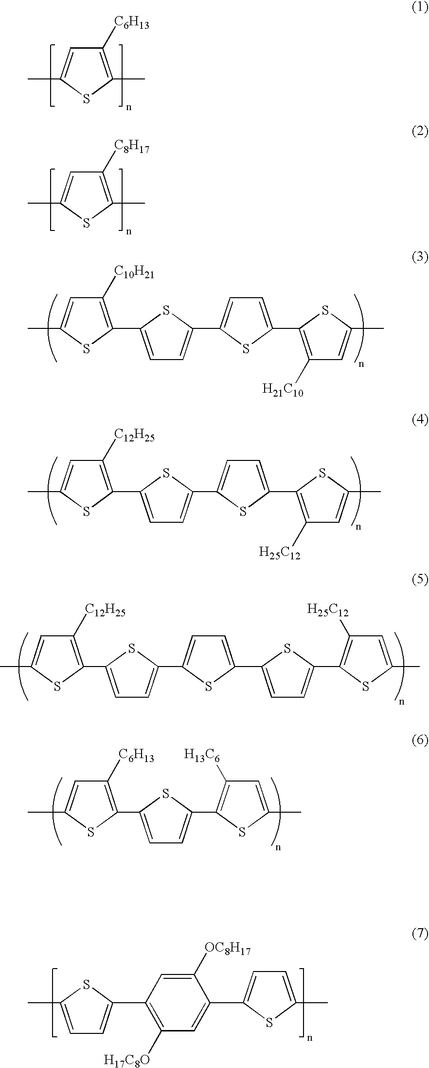
- Polythiophene (4) was prepared in accordance with the procedure of Comparative Example 1 except that the polymerization was conducted in toluene instead of chloroform.
- Polythiophene (4) was prepared in accordance with the procedure of Comparative Example 1 except that the polymerization was conducted in chlorobenzene instead of chloroform.
- the final polythiophene product which was purified by soxhlet extraction with heptane, and then chlorobenzene, showed the following molecular weight properties of M w 22,900; M n 17,300 relative to polystyrene standards.
- Thin film transistor devices were fabricated in accordance with the processes illustrated herein; reference Comparative Example 1. The following average properties were obtained:
- Polythiophene (4) was prepared in dichlorobenzene in accordance with the process of Comparative Example 1 except that dichlorobenzene was utilized instead of chloroform.
- the final polythiophene product which was purified by soxhlet extraction with heptane, and then chlorobenzene, indicated the following molecular weight properties of M w 17,900; M n 11,800 relative to polystyrene standards.
- Thin film transistor devices were then fabricated in accordance with the processes of the above Examples. The following thin film transistor properties were obtained:
- N-bromosuccinimide (4.6 grams, 25.7 mmol) was added to a well-stirred solution of 3,4-dioctylthiophene (3.6 grams, 11.7 mmol) in a mixture of 30 milliliters of dichloromethane and 10 milliliters of acetic acid in a 100 milliliter round bottom flask. The reaction was monitored by thin layer chromatography and was complete in about 35 minutes. The resulting mixture was diluted with 160 milliliters of dichloromethane and filtered to remove succinimide. The filtrate was washed with aqueous 2N sodium hydroxide solution, and then twice with water (2 ⁇ 100 milliliters). After drying with anhydrous sodium sulfate and removal of the solvent, 5.4 grams of 2,5-dibromo-3,4-dioctylthiophene as a light yellow liquid was obtained.
- the polymerization was accomplished in chloroform by the process of Comparative Example 1 except that 2,5-bis(2-thienyl)-3,4-dioctylthiophene was utilized instead of 5,5′-bis(3-dodecyl-2-thienyl)-2,2′-dithiophene.
- the final polythiophene product which was purified by soxhlet extraction with ethyl acetate and chlorobenzene, indicated the following molecular weight properties of M w 49,100; M n 16,300 relative to polystyrene standards.
- Polythiophene (7) was prepared in accordance with the procedure of Comparative Example 3 except that the polymerization was conducted in chlorobenzene instead of chloroform.
- the final polythiophene which was purified by soxhlet extraction with ethyl acetate and chlorobenzene, showed the following molecular weight properties of M w 45,400; M n 18,600 relative to polystyrene standards.
Landscapes
- Chemical & Material Sciences (AREA)
- Physics & Mathematics (AREA)
- Spectroscopy & Molecular Physics (AREA)
- Health & Medical Sciences (AREA)
- Chemical Kinetics & Catalysis (AREA)
- Medicinal Chemistry (AREA)
- Polymers & Plastics (AREA)
- Organic Chemistry (AREA)
- Engineering & Computer Science (AREA)
- Materials Engineering (AREA)
- Thin Film Transistor (AREA)
Abstract

wherein, for example, A is alkyl, alkoxy or derivatives thereof; B is a hydrogen atom, a small substituent like alkyl or alkoxy.
Description

wherein R′ is CF3, alkyl or alkoxy; and y and z represent the number of repeating segments; and in U.S. Ser. No. 10/392,639, filed concurrently herewith on Fluorinated Polythiophene and Devices Thereof, the disclosure of which is totally incorporated herein by reference, is an electronic device comprised of a polythiophene

wherein R is an alkyl or alkoxy; x represents the number of R groups; R′ is CF3, alkoxy or alkyl; y and z represent the number of segments; and a and b are the mole fractions of each moiety, respectively, wherein the sum of a+b is equal to about 1.

wherein, for example, A is a long side-chain comprising, for example, alkyl, alkyl derivatives, alkoxy, and the like, such as alkoxyalkyl; siloxyalkyl, perhaloalkyl, polyether, and the like; B is hydrogen atom or a substituent, such as for example, methyl, ethyl, methoxy, ethoxy, bromo, and the like; and D is selected, for example, from the group consisting of arylene with, for example, from about 6 to about 36 carbon atoms, such as phenylene, biphenylene, phenanthrenylene, dihydrophenanthrenylene, fluorenylene, oligoarylene, methylene, polymethylene, dialkylmethylene, dioxyalkylene, dioxyarylene, oligoethylene oxide, and the like. The long side-chain, A, is preferably one that contains, for example, from about 5 to about 25 atoms, and the small substituent, B, contains from 1 to about 3 carbon atoms. Illustrative examples of A of the 2,5-thienylene moiety (I) include alkyl with, for example, from about 1 to about 25 carbon atoms, and more specifically, from about 5 to about 12 carbon atoms, such as pentyl, hexyl, heptyl, octyl, nonyl, decyl, undecyl, dodecyl, isomeric forms thereof, mixtures thereof, and the like; alkoxy and alkoxyalkyl with, for example, from about 5 to about 25 carbon atoms, such as for example pentyloxy, hexyloxy, heptyloxy, ocytyloxy, methoxybutyl, methoxybutoxy, methoxyhexyl, methoxyheptyl, and the like; and polyether chains, such as polyethylene oxide; perhaloalkyl, such as perfluoroalkyl, and the like.

wherein R is alkyl, alkoxy, or derivatives thereof of, for example, from about 1, and more specifically, about 5 to about 25 carbon atoms; R′ is hydrogen, halogen, alkyl, alkoxy, or the derivatives thereof of, for example, from about 1 to about 25 carbon atoms in length; a and b represent the number of segments, and for example, are independently 1 or 2; Z is a divalent conjugated linkage which may also contain substituted and/or nonsubstituted 2,5-thienylene (or 2,5-thiophenediyl) moieties, and other aromatic units such as arylene, furandiyl, pyrrolediyl, pyridinediyl, benzofurandiyl, dibenzofurandiyl, benzothiophenediyl, dibenzothiophenediyl, carbazolediyl, and the like; and x and y represent the number of segments, such as for example, a number of from 0 to about 3.

wherein R is a suitable substituent, such as alkyl, alkoxy, or derivatives thereof of, for example, from about 5 to about 25 carbon atoms; R′ is a suitable substituent, such as hydrogen, halogen, alkyl, alkoxy, or derivatives thereof of, for example, from about 1 to about 25 carbon atoms in length; a and b represent the number of R groups, and are, for example, independently 1 or 2; Z is a divalent conjugated linkage which may also contain substituted and/or non-substituted 2,5-thienylene (or 2,5-thiophenediyl) moieties, and other aromatic units such as arylene, furandiyl, pyrrolediyl, pyridinediyl, benzofurandiyl, dibenzofurandiyl, benzothiophenediyl, dibenzothiophenediyl, dialkylaminoarylene, carbazolediyl, and the like; x and y represent the number of segments, and for example, are each from 0 to about 3; and n is the degree of polymerization; the number average molecular weight (Mn) of the polythiophenes can be, for example, from about 2,000 to about 100,000, and more specifically, from about 4,000 to about 50,000, and the weight average molecular weight (Mw) thereof can be from about 4,000 to about 500,000, and more specifically, from about 5,000 to about 100,000 both as measured by gel permeation chromatography using polystyrene standards; a device containing a polythiophene of the formula illustrated herein, and wherein when a and/or b are equal to 2, reference substituent R or R′ may form a cyclic structure with the thienylene ring, see for example illustrative Formulas (17) and (18); a thin film transistor device comprised of a substrate, a gate electrode, a gate dielectric layer, a source electrode and a drain electrode, and in contact with the source/drain electrodes and the gate dielectric layer, a semiconductor layer comprised of polythiophene (IV), and wherein R is alkyl with about 5 to about 25 carbon atoms, R′ is hydrogen, halogen, alkyl, alkoxy, or derivatives thereof of from about 1 to about 25 carbon atoms; a and b are 1; Z contains one or more 2,5-thienylene rings and/or arylene rings, and n is 0 or 1; a thin film transistor device containing a semiconductor polythiophene (IV) prepared by the aromatic solvent processes illustrated herein, and which polythiophene has a number average molecular weight (Mn) of from about 2,000 to about 100,000; a weight average molecular weight (Mw) of from about 4,000 to over 500,000, both Mw and Mn being measured by gel permeation chromatography using polystyrene standards; a polythiophene containing device wherein R and/or R′ is alkyl containing from 6 to about 15 carbon atoms; Mn is from about 4,000 to about 50,000, and Mw is from about 5,000 to about 100,000; a polythiophene containing device wherein the alkyl side chain R and/or R′ contains from 6 to about 12 carbon atoms; a polythiophene containing device wherein R is selected from pentyl, hexyl, heptyl, octyl, nonyl, decyl, undecyl, or dodecyl, and R′ is selected from hydrogen, methyl, ethyl, methoxy, ethoxy, and propyl; a device wherein Z contains one or more substituted and/or non-substituted 2,5-thienylene rings; a device of the formulas illustrated herein wherein Z contains aromatic rings selected from the group consisting of 2,5-thienylene, 3-alkyl-2,5-thienylene, 3,4-dialkyl-2,5-thienylene, phenylene, alkylphenylene, dialkylphenylene, alkoxyphenylene, dialkoxyphenylene, biphenylene, phenanthrenylene, 9,10-dihydrophenanthrenylene, fluorenylene, and the like; a thin film transistor containing a polythiophene prepared with a chlorinated aromatic solvent, such as chlorobenzene, dichlorobenzene, trichlorobenzene, and chloronaphthalene; a thin film transistor containing a polythiophene prepared in tetrahydronaphthalene; a thin film transistor containing a polythiophene prepared in chlorobenzene, or dichlorobenzene; a device containing a polythiophene prepared in a chlorinated aromatic solvent and which polythiophene has a Mn of from about 2,000 to about 50,000, and a Mw of from about 4,000 to about 100,000; a polythiophene containing device wherein the polythiophene possesses a Mn of from about 2,000 to about 100,000, and a Mw of from about 4,000 to about 200,000; a polythiophene containing device wherein the polythiophene prepared in a chlorinated aromatic solvent or tetrahydronaphthalene is selected from the group consisting of Formulas (1) to (21), and wherein n represents the number of segments, such as a number of from about 10 to about 1,000


a thin film transistor device wherein the polythiophene is selected from the group consisting of Formulas (3) to (14), and wherein n represents the number of segments, such as from about 10 to about 1,000,


a device wherein the polythiophene is prepared in a suitable aromatic solvent, and which polythiophene is selected from the group consisting of Formulas (3) to (14), and wherein n is a number of from about 20 to about 500


a device wherein the polythiophene is prepared in a chlorinated aromatic solvent, and which polythiophene is selected from the group consisting of Formula (3) to Formula (12), and wherein n is a number of from about 20 to about 100


a device wherein the polythiophene is prepared in chlorobenzene, and which polythiophene is of Formulas (3), (4), (5), (10), (11), (12), (13), or (14) wherein n is as illustrated herein

a device containing a polythiophene prepared by a metal halide polymerization in an aromatic solvent, and which polythiophene is comprised of one or more monomer units selected from the group consisting of a 2,5-thienylene segment (I), and a 2,5-thienylene segment (II)

wherein A is alkyl, a halide, or alkoxy; B is a hydrogen atom, a halide, an alkyl or an alkoxy; and D is a divalent linkage for (I) and (II); an electronic device containing a polythiophene prepared by a metal halide-mediated coupling polymerization in a halogenated aromatic solvent or a hydronaphthalene, and which polythiophene is derived from a monomer segment of Formula (III)

wherein R is alkyl or alkoxy; R′ is hydrogen, alkoxy, halogen, or alkyl; a and b represent the number of R and R′ substituents; Z is a divalent conjugated linkage, and x and y represent the number of segments; a device wherein the divalent linkage, Z, contains one or more segments selected from the group consisting of 2,5-thienylene, arylene, furandiyl, pyrrolediyl, pyridinediyl, benzofurandiyl, dibenzofurandiyl, benzothiophenediyl, dibenzothiophenediyl, dialkylaminoarylene, carbazolediyl, and the like; a thin film transistor containing a polythiophene of Formulas (1) to (18); a thin film transistor containing a polythiophene generated from the polymerization of a monomer of 3-alkylthiophene, 2,5-bis(2-thienyl)-3,4-dialkylthiophene, 2,5-bis(2-thienyl)-3,4-dialkoxythiophene, 2,5-bis(3-alkyl-2-thienyl)thiophene, 2,5-bis(3-alkoxy-2-thienyl)thiophene, 5,5′-bis(3-alkyl-2-thienyl)-2,2′-dithiophene, 5,5′-bis(3-alkoxy-2-thienyl)-2,2′-dithiophene, 1,4-bis(2-thienyl)-2,5-dialkylbenzene, 1,4-bis(2-thienyl)-2,5-dialkoxybenzene, 3,4-ethylenedioxythiophene, 3,4-(2,2-dialkylpropylene-1,3-dioxy)thiophene, or 3-methyl-4-alkoxythiophene; a thin film transistor wherein the substrate is a polyester, or a polycarbonate; the gate source and drain electrodes are each independently comprised of gold, nickel, aluminum, platinum, indium titanium oxide, or a conductive polymer, and the dielectric layer is comprised of silicon nitride or silicon oxide; a thin film transistor wherein the substrate is glass or a plastic sheet; the gate, source and drain electrodes are each comprised of gold, and the dielectric layer is comprised of the organic polymer poly(methacrylate), or poly(vinyl phenol); a device wherein the polythiophene layer is formed by solution processes of spin coating, stamp printing, screen printing, or jet printing; a device wherein the gate, source and drain electrodes, the dielectric, and semiconductor layers are formed by solution processes of spin coating, solution casting, stamp printing, screen printing, or jet printing; and a thin film transistor wherein the substrate is a polyester, or polycarbonate, the gate, source and drain electrodes are fabricated from the organic conductive polymer polystyrene sulfonate-doped poly(3,4-ethylene dioxythiophene) or from a conductive ink/paste compound of a colloidal dispersion of silver in a polymer binder, and the gate dielectric layer is an organic polymer or an inorganic oxide particle-polymer composite.


wherein R, R′, a, b, x, and y are as illustrated herein, and n is the degree or amount of polymerization.
I SD =C iμ(W/2L) (V G −V T)2 (1)
where ISD is the drain current at the saturated regime; W and L are, respectively) the semiconductor channel width and length; Ci is the capacitance per unit area of the gate dielectric layer, and VG and VT are, respectively, the gate voltage and threshold voltage. VT of the device was determined from the relationship between the square root of ISD at the saturated regime and VG of the device by extrapolating the measured data to ISD=0.
| Mobility: | 0.009-0.02 cm2/V · s | ||
| On/off ratio: | 1-5.1 × 10⁶ | ||
| Mobility: | 2.1-4.5 × 10⁻⁴ cm2/V · s | ||
| On/off ratio: | 103-104 | ||
| Mobility: | 0.015-0.04 cm2/V · s | ||
| On/off ratio: | 2.5-7.1 × 10⁶ | ||
| Mobility: | 0.05-0.12 cm2/V · s | ||
| On/off ratio: | 0.9-4.7 × 10⁷ | ||
| Mobility: | 0.013-0.03 cm2/V · s | ||
| On/off ratio: | 1.5-6 × 10⁶ | ||
| Mobility: | 0.049-0.082 cm2/V · s | ||
| On/off ratio: | 0.8-2 × 10⁷ | ||
| Mobility: | 0.001-0.003 cm2/V · s | ||
| On/off ratio: | 1.5-2.6 × 10⁵ | ||
Thermal annealing of the devices in accordance with the procedure of Comparative Example 1 resulted in lower mobility and a poor current on/off ratio.
| Mobility: | 0.006-0.01 cm2/V · s | ||
| On/off ratio: | 0.8-2.1 × 10⁶ | ||
Claims (37)


Priority Applications (2)
| Application Number | Priority Date | Filing Date | Title |
|---|---|---|---|
| US10/392,592 US6897284B2 (en) | 2003-03-19 | 2003-03-19 | Polythiophenes and devices thereof |
| US11/032,711 US7112649B2 (en) | 2003-03-19 | 2005-01-10 | Polythiophenes and devices thereof |
Applications Claiming Priority (1)
| Application Number | Priority Date | Filing Date | Title |
|---|---|---|---|
| US10/392,592 US6897284B2 (en) | 2003-03-19 | 2003-03-19 | Polythiophenes and devices thereof |
Related Child Applications (1)
| Application Number | Title | Priority Date | Filing Date |
|---|---|---|---|
| US11/032,711 Continuation US7112649B2 (en) | 2003-03-19 | 2005-01-10 | Polythiophenes and devices thereof |
Publications (2)
| Publication Number | Publication Date |
|---|---|
| US20040186265A1 US20040186265A1 (en) | 2004-09-23 |
| US6897284B2 true US6897284B2 (en) | 2005-05-24 |
Family
ID=32987928
Family Applications (2)
| Application Number | Title | Priority Date | Filing Date |
|---|---|---|---|
| US10/392,592 Expired - Lifetime US6897284B2 (en) | 2003-03-19 | 2003-03-19 | Polythiophenes and devices thereof |
| US11/032,711 Expired - Lifetime US7112649B2 (en) | 2003-03-19 | 2005-01-10 | Polythiophenes and devices thereof |
Family Applications After (1)
| Application Number | Title | Priority Date | Filing Date |
|---|---|---|---|
| US11/032,711 Expired - Lifetime US7112649B2 (en) | 2003-03-19 | 2005-01-10 | Polythiophenes and devices thereof |
Country Status (1)
| Country | Link |
|---|---|
| US (2) | US6897284B2 (en) |
Cited By (17)
| Publication number | Priority date | Publication date | Assignee | Title |
|---|---|---|---|---|
| US20050043504A1 (en) * | 2003-08-22 | 2005-02-24 | Xerox Corporation | Polymers |
| US20050159580A1 (en) * | 2003-03-19 | 2005-07-21 | Xerox Corporation | Polythiophenes and devices thereof |
| US20050277760A1 (en) * | 2004-06-10 | 2005-12-15 | Xerox Corporation | Device with small molecular thiophene compound having divalent linkage |
| US20050276981A1 (en) * | 2004-06-10 | 2005-12-15 | Xerox Corporation | Device with small molecular thiophene compound |
| US20050280504A1 (en) * | 2004-06-22 | 2005-12-22 | Vubiq Incorporated, A Nevada Corporation | RFID system utilizing parametric reflective technology |
| US20060076050A1 (en) * | 2004-09-24 | 2006-04-13 | Plextronics, Inc. | Heteroatomic regioregular poly(3-substitutedthiophenes) for photovoltaic cells |
| US20060151779A1 (en) * | 2005-01-07 | 2006-07-13 | Samsung Electronics Co., Ltd. | Novel thiophene-thiazole derivatives and organic thin film transistors using the same |
| US20070077681A1 (en) * | 2005-09-30 | 2007-04-05 | Florian Dotz | Liquid phase fabrication of active devices including organic semiconductors |
| US20070117961A1 (en) * | 2005-11-18 | 2007-05-24 | Xerox Corporation | Polythiophene processes |
| WO2007109545A3 (en) * | 2006-03-16 | 2008-10-09 | Univ California | Copolymers of alkoxythiophene |
| US7488834B2 (en) | 2005-09-30 | 2009-02-10 | Alcatel-Lucent Usa Inc. | Organic semiconductors |
| US20090089111A1 (en) * | 2007-09-27 | 2009-04-02 | Xerox Corporation. | System and method for automating product life cycle management |
| US20100093129A1 (en) * | 2008-10-09 | 2010-04-15 | Xerox Corporation | Semiconducting ink formulation |
| US20110049480A1 (en) * | 2009-08-25 | 2011-03-03 | Samsung Electronics Co., Ltd. | Organic semiconductor polymer and transistor including the same |
| US8784690B2 (en) | 2010-08-20 | 2014-07-22 | Rhodia Operations | Polymer compositions, polymer films, polymer gels, polymer foams, and electronic devices containing such films, gels and foams |
| CN108550525A (en) * | 2018-05-28 | 2018-09-18 | 武汉新芯集成电路制造有限公司 | Floating boom preparation method |
| US11216625B2 (en) | 2018-12-05 | 2022-01-04 | Vubiq Networks, Inc. | High bit density millimeter wave RFID systems, devices, and methods of use thereof |
Families Citing this family (21)
| Publication number | Priority date | Publication date | Assignee | Title |
|---|---|---|---|---|
| JP4194436B2 (en) * | 2003-07-14 | 2008-12-10 | キヤノン株式会社 | Field effect organic transistor |
| DE602004016858D1 (en) * | 2003-08-06 | 2008-11-13 | Merck Patent Gmbh | PROCESS FOR THE PRODUCTION OF REGIOREGULAR POLYMERS |
| DE602005020175D1 (en) * | 2004-09-24 | 2010-05-06 | Plextronics Inc | HETEROATOMIC REGIOREGULAR POLY (3-SUBTITUDE THIOPHENE) IN ELECTROLUMINESCENCE ELEMENTS |
| US7619242B2 (en) | 2005-02-25 | 2009-11-17 | Xerox Corporation | Celluloses and devices thereof |
| US7321021B2 (en) * | 2005-03-22 | 2008-01-22 | Xerox Corporation | Removing impurities from polythiophene |
| KR101102158B1 (en) * | 2005-05-11 | 2012-01-02 | 삼성전자주식회사 | Novel organic polymer semiconductor, method for forming organic polymer semiconductor thin film using same and organic thin film transistor using same |
| GB2441702B (en) * | 2005-06-21 | 2010-10-27 | Konica Minolta Holdings Inc | Method for forming thin organic semiconductor material film and method for producing organic thin-film transistor |
| JP5245116B2 (en) * | 2005-06-24 | 2013-07-24 | コニカミノルタ株式会社 | Method for forming organic semiconductor film and method for producing organic thin film transistor |
| CN100555702C (en) * | 2006-04-29 | 2009-10-28 | 中国科学院长春应用化学研究所 | Organic semiconductor crystal thin film and method for preparation of weak oriented epitaxial growth and application |
| WO2008067443A1 (en) * | 2006-11-29 | 2008-06-05 | Board Of Governors For Higher Education, | Aerobic oxidative coupling for the formation biaryls |
| US8044389B2 (en) * | 2007-07-27 | 2011-10-25 | The Regents Of The University Of California | Polymer electronic devices by all-solution process |
| CN101945922A (en) * | 2008-02-18 | 2011-01-12 | 住友化学株式会社 | Composition and organic photoelectric conversion element using same |
| US8164089B2 (en) * | 2009-10-08 | 2012-04-24 | Xerox Corporation | Electronic device |
| KR101135618B1 (en) * | 2010-02-25 | 2012-04-17 | 한양대학교 산학협력단 | Method of preparing polythiophene and polythiophene prepared by same |
| WO2012021301A1 (en) * | 2010-08-13 | 2012-02-16 | Massachusetts Institute Of Technology | Interconnection between conducting polymer materials |
| CN104395427B (en) | 2012-06-04 | 2016-05-11 | 沙特阿拉伯石油公司 | The manufacture of the polymer of thiophene, benzothiophene and their alkyl derivative |
| KR101461136B1 (en) * | 2012-10-18 | 2014-11-13 | 광주과학기술원 | Organic semiconductor polymer comprising semi-fluoroalkyl group, and organic thin-film transistor comprising the same |
| US8569443B1 (en) | 2012-12-18 | 2013-10-29 | Xerox Corporation | Copolythiophene semiconductors for electronic device applications |
| EP3400619A4 (en) * | 2015-12-28 | 2019-11-27 | Nissan Chemical Industries, Ltd. | NANOPARTICLE CONDUCTIVE POLYMER COMPOSITE FOR USE IN ORGANIC ELECTRONIC DEVICES |
| CN109713287B (en) * | 2019-01-02 | 2022-02-01 | 齐鲁工业大学 | Polythiophene derived sulfur-doped carbon sodium ion battery negative electrode material |
| US20220367814A1 (en) * | 2019-05-06 | 2022-11-17 | Raynergy Tek Inc. | Photoactive composition |
Citations (8)
| Publication number | Priority date | Publication date | Assignee | Title |
|---|---|---|---|---|
| US5069823A (en) * | 1989-03-29 | 1991-12-03 | Agency Of Industrial Science And Technology | Thiophene compound and method for production thereof |
| US5347144A (en) * | 1990-07-04 | 1994-09-13 | Centre National De La Recherche Scientifique (Cnrs) | Thin-layer field-effect transistors with MIS structure whose insulator and semiconductor are made of organic materials |
| US5619357A (en) | 1995-06-06 | 1997-04-08 | International Business Machines Corporation | Flat panel display containing black matrix polymer |
| US5777070A (en) | 1997-10-23 | 1998-07-07 | The Dow Chemical Company | Process for preparing conjugated polymers |
| US5969376A (en) | 1996-08-23 | 1999-10-19 | Lucent Technologies Inc. | Organic thin film transistor having a phthalocyanine semiconductor layer |
| US6107117A (en) | 1996-12-20 | 2000-08-22 | Lucent Technologies Inc. | Method of making an organic thin film transistor |
| US6320200B1 (en) * | 1992-06-01 | 2001-11-20 | Yale University | Sub-nanoscale electronic devices and processes |
| US6621099B2 (en) * | 2002-01-11 | 2003-09-16 | Xerox Corporation | Polythiophenes and devices thereof |
Family Cites Families (2)
| Publication number | Priority date | Publication date | Assignee | Title |
|---|---|---|---|---|
| US6897284B2 (en) * | 2003-03-19 | 2005-05-24 | Xerox Corporation | Polythiophenes and devices thereof |
| US6855951B2 (en) * | 2003-03-19 | 2005-02-15 | Xerox Corporation | Fluorinated polythiophenes and devices thereof |
-
2003
- 2003-03-19 US US10/392,592 patent/US6897284B2/en not_active Expired - Lifetime
-
2005
- 2005-01-10 US US11/032,711 patent/US7112649B2/en not_active Expired - Lifetime
Patent Citations (9)
| Publication number | Priority date | Publication date | Assignee | Title |
|---|---|---|---|---|
| US5069823A (en) * | 1989-03-29 | 1991-12-03 | Agency Of Industrial Science And Technology | Thiophene compound and method for production thereof |
| US5347144A (en) * | 1990-07-04 | 1994-09-13 | Centre National De La Recherche Scientifique (Cnrs) | Thin-layer field-effect transistors with MIS structure whose insulator and semiconductor are made of organic materials |
| US6320200B1 (en) * | 1992-06-01 | 2001-11-20 | Yale University | Sub-nanoscale electronic devices and processes |
| US5619357A (en) | 1995-06-06 | 1997-04-08 | International Business Machines Corporation | Flat panel display containing black matrix polymer |
| US5969376A (en) | 1996-08-23 | 1999-10-19 | Lucent Technologies Inc. | Organic thin film transistor having a phthalocyanine semiconductor layer |
| US6150191A (en) | 1996-08-23 | 2000-11-21 | Lucent Technologies Inc. | Method of making an organic thin film transistor and article made by the method |
| US6107117A (en) | 1996-12-20 | 2000-08-22 | Lucent Technologies Inc. | Method of making an organic thin film transistor |
| US5777070A (en) | 1997-10-23 | 1998-07-07 | The Dow Chemical Company | Process for preparing conjugated polymers |
| US6621099B2 (en) * | 2002-01-11 | 2003-09-16 | Xerox Corporation | Polythiophenes and devices thereof |
Non-Patent Citations (6)
| Title |
|---|
| Beng S. Ong et al., U.S. Appl. No. 10/042,342 on Polythiophenes and Devices Thereof, filed Jan. 11, 2002. |
| Beng S. Ong et al., U.S. Appl. No. 10/042,356 on Polythiophenes and Devices Thereof, filed Jan. 11, 2002. |
| Beng S. Ong et al., U.S. Appl. No. 10/042,357 on Polythiophenes and Devices Thereof, filed Jan. 11, 2002. |
| Beng S. Ong et al., U.S. Appl. No. 10/042,358 on Polythiophenes and Devices Thereof, filed Jan. 11, 2002. |
| Beng S. Ong et al., U.S. Appl. No. 10/042,359 on Polythiophenes and Devices Thereof, filed Jan. 11, 2002. |
| Beng S. Ong et al., U.S. Appl. No. 10/042,360 on Polythiophenes and Devices Thereof, filed Jan. 11, 2002. |
Cited By (40)
| Publication number | Priority date | Publication date | Assignee | Title |
|---|---|---|---|---|
| US7112649B2 (en) * | 2003-03-19 | 2006-09-26 | Xerox Corporation | Polythiophenes and devices thereof |
| US20050159580A1 (en) * | 2003-03-19 | 2005-07-21 | Xerox Corporation | Polythiophenes and devices thereof |
| US20070093641A1 (en) * | 2003-08-22 | 2007-04-26 | Xerox Corporation | Polymers |
| US20050043504A1 (en) * | 2003-08-22 | 2005-02-24 | Xerox Corporation | Polymers |
| US7449542B2 (en) | 2003-08-22 | 2008-11-11 | Xerox Corporation | Polymers |
| US7169883B2 (en) * | 2003-08-22 | 2007-01-30 | Xerox Corporation | Polymers |
| US20050276981A1 (en) * | 2004-06-10 | 2005-12-15 | Xerox Corporation | Device with small molecular thiophene compound |
| US20080108833A1 (en) * | 2004-06-10 | 2008-05-08 | Xerox Corporation | Small molecular thiophene compound |
| US20080108834A1 (en) * | 2004-06-10 | 2008-05-08 | Xerox Corporation | Small molecular thiophene compound having divalent linkage |
| US7700787B2 (en) | 2004-06-10 | 2010-04-20 | Xerox Corporation | Small molecular thiophene compound |
| US7312469B2 (en) * | 2004-06-10 | 2007-12-25 | Xerox Corporation | Device with small molecular thiophene compound |
| US20050277760A1 (en) * | 2004-06-10 | 2005-12-15 | Xerox Corporation | Device with small molecular thiophene compound having divalent linkage |
| US7834199B2 (en) | 2004-06-10 | 2010-11-16 | Xerox Corporation | Small molecular thiophene compound having divalent linkage |
| US7294850B2 (en) * | 2004-06-10 | 2007-11-13 | Xerox Corporation | Device with small molecular thiophene compound having divalent linkage |
| US20050280539A1 (en) * | 2004-06-22 | 2005-12-22 | Pettus Michael G | RFID system utilizing parametric reflective technology |
| US7498940B2 (en) | 2004-06-22 | 2009-03-03 | Vubiq, Inc. | RFID system utilizing parametric reradiated technology |
| US20050280504A1 (en) * | 2004-06-22 | 2005-12-22 | Vubiq Incorporated, A Nevada Corporation | RFID system utilizing parametric reflective technology |
| US7460014B2 (en) | 2004-06-22 | 2008-12-02 | Vubiq Incorporated | RFID system utilizing parametric reflective technology |
| US7790979B2 (en) | 2004-09-24 | 2010-09-07 | Plextronics, Inc. | Heteroatomic regioregular poly(3-substitutedthiophenes) for photovoltaic cells |
| US20060076050A1 (en) * | 2004-09-24 | 2006-04-13 | Plextronics, Inc. | Heteroatomic regioregular poly(3-substitutedthiophenes) for photovoltaic cells |
| US20060151779A1 (en) * | 2005-01-07 | 2006-07-13 | Samsung Electronics Co., Ltd. | Novel thiophene-thiazole derivatives and organic thin film transistors using the same |
| US20070077681A1 (en) * | 2005-09-30 | 2007-04-05 | Florian Dotz | Liquid phase fabrication of active devices including organic semiconductors |
| US7569415B2 (en) | 2005-09-30 | 2009-08-04 | Alcatel-Lucent Usa Inc. | Liquid phase fabrication of active devices including organic semiconductors |
| US7488834B2 (en) | 2005-09-30 | 2009-02-10 | Alcatel-Lucent Usa Inc. | Organic semiconductors |
| US7314908B2 (en) | 2005-11-18 | 2008-01-01 | Xerox Corporation | Polythiophene processes |
| US20070117961A1 (en) * | 2005-11-18 | 2007-05-24 | Xerox Corporation | Polythiophene processes |
| US8530594B2 (en) | 2006-03-16 | 2013-09-10 | The Regents Of The University Of California | Copolymers of alkoxythiophene |
| US20090095343A1 (en) * | 2006-03-16 | 2009-04-16 | The Regents Of The University Of California | Copolymers of alkoxythiophene |
| WO2007109545A3 (en) * | 2006-03-16 | 2008-10-09 | Univ California | Copolymers of alkoxythiophene |
| US20090089111A1 (en) * | 2007-09-27 | 2009-04-02 | Xerox Corporation. | System and method for automating product life cycle management |
| US20100093129A1 (en) * | 2008-10-09 | 2010-04-15 | Xerox Corporation | Semiconducting ink formulation |
| US8052895B2 (en) | 2008-10-09 | 2011-11-08 | Xerox Corporation | Semiconducting ink formulation |
| US20110049480A1 (en) * | 2009-08-25 | 2011-03-03 | Samsung Electronics Co., Ltd. | Organic semiconductor polymer and transistor including the same |
| US8405071B2 (en) | 2009-08-25 | 2013-03-26 | Samsung Electronics Co., Ltd. | Organic semiconductor polymer and transistor including the same |
| US8784690B2 (en) | 2010-08-20 | 2014-07-22 | Rhodia Operations | Polymer compositions, polymer films, polymer gels, polymer foams, and electronic devices containing such films, gels and foams |
| US9378859B2 (en) | 2010-08-20 | 2016-06-28 | Rhodia Operations | Polymer compositions, polymer films, polymer gels, polymer foams, and electronic devices containing such films, gels and foams |
| US9552903B2 (en) | 2010-08-20 | 2017-01-24 | Rhodia Operations | Polymer compositions, polymer films, polymer gels, polymer foams, and electronic devices containing such films, gels and foams |
| CN108550525A (en) * | 2018-05-28 | 2018-09-18 | 武汉新芯集成电路制造有限公司 | Floating boom preparation method |
| US11107697B2 (en) | 2018-05-28 | 2021-08-31 | Wuhan Xinxin Semiconductor Manufacturing Co., Ltd. | Floating gate fabrication method |
| US11216625B2 (en) | 2018-12-05 | 2022-01-04 | Vubiq Networks, Inc. | High bit density millimeter wave RFID systems, devices, and methods of use thereof |
Also Published As
| Publication number | Publication date |
|---|---|
| US20040186265A1 (en) | 2004-09-23 |
| US7112649B2 (en) | 2006-09-26 |
| US20050159580A1 (en) | 2005-07-21 |
Similar Documents
| Publication | Publication Date | Title |
|---|---|---|
| US6897284B2 (en) | Polythiophenes and devices thereof | |
| US7767999B2 (en) | Polythiophenes and devices thereof | |
| US6872801B2 (en) | Polythiophenes and devices thereof | |
| US7781564B2 (en) | Polythiophenes and devices thereof | |
| US6992167B2 (en) | Polythiophenes and devices thereof | |
| US7250625B2 (en) | Polythiophenes and electronic devices generated therefrom | |
| US20030136958A1 (en) | Polythiophenes and devices thereof | |
| US20030171531A1 (en) | Polthiophenes and devices thereof | |
| US7049629B2 (en) | Semiconductor polymers and devices thereof | |
| US6855951B2 (en) | Fluorinated polythiophenes and devices thereof | |
| US6960643B2 (en) | Fluorinated polythiophenes and devices thereof | |
| US7449542B2 (en) | Polymers | |
| Liu et al. | Ong |
Legal Events
| Date | Code | Title | Description |
|---|---|---|---|
| AS | Assignment |
Owner name: XEROX CORPORATION, CONNECTICUT Free format text: ASSIGNMENT OF ASSIGNORS INTEREST;ASSIGNORS:LIU, PING;WU, YILIANG;JIANG, LU;AND OTHERS;REEL/FRAME:013891/0860;SIGNING DATES FROM 20021127 TO 20021211 |
|
| AS | Assignment |
Owner name: JPMORGAN CHASE BANK, AS COLLATERAL AGENT, TEXAS Free format text: SECURITY AGREEMENT;ASSIGNOR:XEROX CORPORATION;REEL/FRAME:015134/0476 Effective date: 20030625 Owner name: JPMORGAN CHASE BANK, AS COLLATERAL AGENT,TEXAS Free format text: SECURITY AGREEMENT;ASSIGNOR:XEROX CORPORATION;REEL/FRAME:015134/0476 Effective date: 20030625 |
|
| STCF | Information on status: patent grant |
Free format text: PATENTED CASE |
|
| CC | Certificate of correction | ||
| FPAY | Fee payment |
Year of fee payment: 4 |
|
| REMI | Maintenance fee reminder mailed | ||
| FPAY | Fee payment |
Year of fee payment: 8 |
|
| SULP | Surcharge for late payment |
Year of fee payment: 7 |
|
| CC | Certificate of correction | ||
| AS | Assignment |
Owner name: XEROX CORPORATION, NEW YORK Free format text: RELEASE BY SECURED PARTY;ASSIGNOR:JPMORGAN CHASE BANK, N.A.;REEL/FRAME:032893/0588 Effective date: 20061204 |
|
| FPAY | Fee payment |
Year of fee payment: 12 |
|
| AS | Assignment |
Owner name: XEROX CORPORATION, CONNECTICUT Free format text: RELEASE BY SECURED PARTY;ASSIGNOR:JPMORGAN CHASE BANK, N.A. AS SUCCESSOR-IN-INTEREST ADMINISTRATIVE AGENT AND COLLATERAL AGENT TO JPMORGAN CHASE BANK;REEL/FRAME:066728/0193 Effective date: 20220822 |
|
| AS | Assignment |
Owner name: CITIBANK, N.A., AS AGENT, DELAWARE Free format text: SECURITY INTEREST;ASSIGNOR:XEROX CORPORATION;REEL/FRAME:062740/0214 Effective date: 20221107 |
|
| AS | Assignment |
Owner name: XEROX CORPORATION, CONNECTICUT Free format text: RELEASE OF SECURITY INTEREST IN PATENTS AT R/F 062740/0214;ASSIGNOR:CITIBANK, N.A., AS AGENT;REEL/FRAME:063694/0122 Effective date: 20230517 |