US6879178B1 - Measuring current on a die - Google Patents
Measuring current on a die Download PDFInfo
- Publication number
- US6879178B1 US6879178B1 US10/745,101 US74510103A US6879178B1 US 6879178 B1 US6879178 B1 US 6879178B1 US 74510103 A US74510103 A US 74510103A US 6879178 B1 US6879178 B1 US 6879178B1
- Authority
- US
- United States
- Prior art keywords
- voltage
- die
- current
- power input
- power supply
- Prior art date
- Legal status (The legal status is an assumption and is not a legal conclusion. Google has not performed a legal analysis and makes no representation as to the accuracy of the status listed.)
- Expired - Fee Related
Links
Images


Classifications
-
- G—PHYSICS
- G01—MEASURING; TESTING
- G01R—MEASURING ELECTRIC VARIABLES; MEASURING MAGNETIC VARIABLES
- G01R31/00—Arrangements for testing electric properties; Arrangements for locating electric faults; Arrangements for electrical testing characterised by what is being tested not provided for elsewhere
- G01R31/28—Testing of electronic circuits, e.g. by signal tracer
- G01R31/30—Marginal testing, e.g. by varying supply voltage
- G01R31/3004—Current or voltage test
- G01R31/3012—Built-In-Current test [BIC]
Definitions
- FIG. 1 is a schematic block diagram of a circuit board having a central processing unit comprising a semiconductor package and a die that is coupled to a power supply that generates a current that is measured according to the various embodiments of the present invention
- FIG. 2A is a flow chart of an example of a method for determining a current supplied to the die by the power supply of FIG. 1 according to an embodiment of the present invention
- FIG. 2B is a flow chart of an example of one method for determining a voltage supplied to the die by the power supply of FIG. 1 as a portion of the method of FIG. 2A according to an embodiment of the present invention
- FIG. 3 is a graph that illustrates an example of the impedance of a power supply loop associated with the central processing unit circuit board of FIG. 1 as a function of frequency as employed according to various embodiments of the present invention
- FIG. 4 is a graph that illustrates one example of a measured voltage supplied to the die by the power supply of FIG. 1 ;
- FIG. 5 is a graph that illustrates one example of a Fourier transform of the current supplied to the die by the power supply of FIG. 1 calculated according to various embodiments of the present invention
- FIG. 6 is a graph of an example of the current determined by taking an inverse Fourier transform of the Fourier transform of the current illustrated in the graph of FIG. 5 according to an embodiment of the present invention
- FIG. 7 is a schematic block diagram of an example of a computer system that is employed to execute a power supply current calculator to determine the current supplied to the die by the power supply of FIG. 1 according to an embodiment of the present invention.
- FIG. 8 is a flow chart that provides an example of the operation of a power supply current calculator executed in the computer system of FIG. 7 .
- FIG. 1 shown is a schematic block diagram of a central processing unit (CPU) circuit board 100 upon which is mounted a CPU package 103 .
- the CPU package 103 comprises packaging 106 and at least one semiconductor die 109 .
- a power supply 113 is also included on the CPU circuit board 100 .
- the power supply 113 may be located within the CPU package 103 .
- the power supply 113 may be, for example, a voltage regulator or other appropriate device or circuit as can be appreciated by those with ordinary skill in the art.
- the power supply 113 generates voltage V Supply and current I dd that flows to the die 109 .
- the CPU package 103 includes test points 116 that allow the voltage V to be measured across the voltage V dd and the common V ss during operation of the die 109 itself.
- the power supply 113 supplies system voltage V Supply to the die 109 during operation of the die 109 .
- a power supply loop exists that includes the power supply 113 and the conductors that couple the power supply 113 to the power input of the die 109 .
- Such conductors may include, for example, a ground plane (i.e. solid or grid), a power plane (i.e. solid or grid), vias, traces, coupling capacitors, bumps, and/or other elements.
- the voltage V may not equal the voltage V Supply due to the impedance in the conductors between the power supply 113 and the power input of the die 109 and due to other circumstances as can be appreciated by those with ordinary skill in the art.
- the power supply 113 may also provide voltage and current to other components (not shown) in the packaging 106 and on the CPU circuit board 100 .
- conductors are provided that link V dd and V ss to the test points 116 . These conductors make up a transmission line 119 between the voltage V input of the die 109 to the test points 116 .
- the transmission line 119 includes resistance R TL1 .
- a differential probe 123 is employed to obtain a measure of the voltage V.
- the differential probe 123 includes cables that make up a transmission line 126 that is coupled to the inputs of a comparator 129 .
- the transmission line 126 includes resistance R TL2 .
- the transmission line 126 is configured to contact the test points 116 on the CPU package 103 .
- the transmission lines 119 and 126 make up a transmission line 127 between the power input of the die 109 and the inputs of the comparator 129 of the differential probe 123 .
- the resistance of the transmission line 127 is noted as R TL which is the sum of the resistances R TL1 , and R TL2 .
- the characteristic impedance of the transmission lines 119 and 126 are matched so as to minimize reflections at the junction between the transmission lines 119 and 126 as can be appreciated.
- the differential probe 123 may include a terminal resistance R TERM that is coupled across the inputs to the comparator 129 .
- the output of the differential probe 123 is applied to an oscilloscope 131 to view the resulting waveform.
- a voltage V w is specified as the voltage across the terminal resistor R TERM that is input into the comparator 129 .
- the differential probe 123 is employed, for example, to measure the voltage V at the power input of the die 109 .
- the resistance of the termination resistance R TERM is calculated so as to minimize reflection of the voltage signals reaching the comparator 129 . However, given that such reflections are generally of high frequency, the termination resistance R TERM may not be necessary if high frequency reflections or noise is of no concern. In such a case, the high frequency noise may be filtered out of the signal obtained as will be described.
- the transmission line 126 is coupled to the test points 116 .
- the voltage V w is measured over a period of time (V w (t)) and is stored in a memory associated, for example, with the oscilloscope 131 .
- the voltage V(t) may then be calculated from the voltage V w (t), the termination resistance R TERM , and the transmission line resistance R TL of the transmission line 127 .
- the voltage V may be measured and stored as a function of time (V(t)) in a memory associated, for example, with the oscilloscope 131 .
- V(t) the voltage V(t) is the same as the voltage V w (t) measured across the inputs of the comparator 129 since the comparator 129 includes a near infinite input resistance and there is negligible current on the transmission line 127 .
- the voltage V(t) may be stored, for example, on a computer readable medium that is accessed for further analysis and calculation as will be discussed.
- the voltage V(t) may be subjected to filter to eliminate or minimize any unwanted high frequency components when the voltage V(t) is measured without the termination resistance R TERM .
- FIG. 2A shown is a flow chart of one example of a method 130 for obtaining a measure of the current I dd (t) ( FIG. 1 ) as a function of time according to an embodiment of the present invention.
- the impedance of the power supply loop as a function of frequency is obtained.
- the impedance is denoted as Z f ( ⁇ ) herein and includes magnitude and phase.
- the impedance Z f ( ⁇ ) of the power supply loop may be ascertained using other approaches as can be appreciated by those with ordinary skill in the art.
- the predefined computer process may be code that, when executed, implements various functions of the die 109 . Specifically, given that the circuitry of the die 109 comprises a processor circuit, then the computer process that comprises predefined test code is loaded into a memory portion of the die 109 and is executed thereby to create the conditions in which the current I dd includes noise due to the rate of change of the current as a result of the fluctuating load presented by the execution of the computer process.
- the voltage V(t) is measured with the differential probe 123 and is stored for future use.
- the transmission line 126 FIG. 1
- the transmission line 126 FIG. 1
- the voltage V(t) is measured in situ while the die 109 is operation.
- the termination resistance R TERM FIG. 1
- the termination resistance R TERM may or may not be used. If the termination resistance R TERM is not employed, then additional high frequency noise may be detected in the voltage V(t).
- the waveform of the voltage V(t) may be filtered to remove any unwanted high frequency components.
- the termination resistance R TERM may be employed to minimize unwanted reflections that may occur in the transmission line 127 ( FIG. 1 ) of the differential probe 123 ( FIG. 1 ) as will be discussed.
- the Fourier transform of the voltage V(t) is calculated.
- the Fourier transform of the voltage V(t) is denoted herein as F f (V(t)).
- F f V(t)
- a Fourier transform operation may be performed on the data that represents the voltage V(t) determined in box 139 .
- the Fourier component of the current I dd (t) is calculated from the Fourier transform F f V(t)) of the voltage V(t) and the impedance Z f ( ⁇ ).
- F f ( I dd (t )) F f ( V ( t ))/ Z f or its mathematical equivalent.
- the current I dd (t) is determined by calculating the inverse Fourier transform of the Fourier component of the current F f (I dd (t)).
- the data that represents the current I dd (t) may then be stored and analyzed accordingly. Thereafter, the method 130 ends as shown.
- the approach employed above to determine the current I dd (t) is advantageous as it is determined “in situ” as it is derived from the data representing the voltage V(t) that was measured during the execution of the computer process by the die 109 .
- the measurement of the current I dd (t) is non-intrusive in that measuring equipment does not unacceptably alter or distort the voltage V(t) during the operation of the die 109 . Consequently, a relatively accurate measure of the current I dd (t) may be obtained without unacceptable distortion in the current I dd (t) itself.
- the measurement of I dd (t) may be compared with the modeled current to verify that the electrical load represented by the die 109 is within design limits.
- FIG. 2B shown is a flow chart of one example of a method to measure the voltage V(t) ( FIG. 1 ) across the test points 116 ( FIG. 1 ) as described in step 139 ( FIG. 2A ) in a manner that minimizes reflections in the transmission line 127 according to an embodiment of the present invention.
- a measure of the resistance R TL of the transmission line 127 is obtained.
- the resistance R TL of the transmission line 127 may be obtained, for example, using a time domain reflectometer or using other approaches as can be appreciated by those with ordinary skill in the art.
- the resistance R TL is equal to the sum of the resistance R TL of the transmission line 119 and the resistance R TL2 of the transmission line 126 as described above.
- step 156 the terminal resistance R TERM that is to be applied across the inputs of the comparator 129 of the differential probe 123 as shown is calculated so as to minimize reflections in the transmission line 127 of the differential probe 123 .
- step 159 the voltage V w (t) ( FIG. 1 ) is measured in situ for a predefined period of time while the computer process runs on the die 109 ( FIG. 1 ) as was initiated in step 136 .
- the transmission line 126 is coupled to the test points 116 and measurements of the voltage V w (t) are taken while running the computer process on the die 109 (FIG. 1 ).
- step 163 the voltage V(t) is calculated from the probe voltage V w (t), the termination resistance R TERM , and the transmission line resistance R TL .
- the voltage V(t) may be employed to determine the current I dd (t) as described with reference to FIG. 2 A. Thereafter, the method 139 ends as shown.
- the voltage V(t) derived as described above may include some degree of error due to reflections that occur despite the use of the termination resistance R TERM . However, to the extent that the termination resistance R TERM is properly calculated, the degree of error may be minimized such that an acceptable measure of the voltage V(t) is obtained.
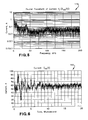
- FIG. 3 is a graph 173 that provides one example of the impedance Z f ( ⁇ ) of a power supply loop measured as described above for specific die 109 . As shown, the impedance Z f ( ⁇ ) varies significantly across the frequency spectrum shown.
- FIG. 4 is a graph 176 that provides one example of the voltage V w (t) measured as described above. In the specific measurement of V w (t) shown is FIG. 4 , the termination resistance R TERM of the differential probe 123 ( FIG. 1 ) employed was 100 Ohms and the transmission line resistance R TL was measured to be 7 Ohms.
- FIG. 5 is a graph 179 that provides one example of the Fourier transform of the current F f (I dd (t)) calculated from the Fourier transform of the voltage F f (V(t)) divided by the impedance Z f ( ⁇ ).
- FIG. 6 is a graph 183 that illustrates an example of the current I dd (t) that is obtained by calculating the inverse Fourier transform of the current F f (I dd (t)) displayed in FIG. 5 .
- the computer system 200 may be, for example, a desktop, laptop, personal digital assistant, or other system with like capability.
- the computer system 200 includes a central processing unit 201 having a processor circuit having a processor 203 and a memory 206 that are both coupled to a local interface 209 .
- the local interface 209 may be, for example, a data bus with an accompanying control/address bus as can be appreciated by those with ordinary skill in the art.
- the processor circuit may be included within the oscilloscope 131 or other device as can be appreciated.
- the computer system 200 includes peripheral devices such as, for example, a display device 213 , a keyboard 216 , and a mouse 219 .
- the computer system 200 may also include other peripheral devices not shown such as, for example, a keypad, touch pad, touch screen, microphone, scanner, joystick, or one or more push buttons, etc.
- the peripheral devices may also include indicator lights, speakers, printers, etc.
- the display device 213 may be, for example, cathode ray tubes (CRTs), liquid crystal display screens, gas plasma-based flat panel displays, or other types of display devices, etc.
- each of the peripheral devices associated with the computer system 200 may be included within the device itself such as is the case, for example, with a laptop, personal digital assistant or other device.
- Stored in the memory 206 and executable by the processor 203 are a number of components including, for example, an operating system 223 and a power supply current calculator 226 .
- various data files may be stored in the memory 206 and accessed by various systems executed by the processor 203 such as, for example, a voltage V(t) data file 229 , a voltage V w (t) data file 233 , and an impedance Z f data file 236 .
- other systems and data files may be stored in the memory 206 .
- the voltage V(t) data file 229 represents the voltage V(t) measured as discussed above.
- the voltage V w (t) data file 229 represents the voltage measured by the differential probe 123 across the terminal resistance R TERM as described above.
- the voltage V(t) data file 229 and the voltage V w (t) data file 229 may be generated using appropriate data capture equipment and the differential probe 123 as discussed above and are stored in the memory 206 to be accessed by the power supply current calculator 223 .
- the impedance Z f data file 236 may be generated as described above and ultimately stored in the memory 206 to be accessed by the power supply current calculator 223 .
- the memory 206 is defined herein as both volatile and nonvolatile memory and data storage components. Volatile components are those that do not retain data values upon loss of power. Nonvolatile components are those that retain data upon a loss of power.
- the memory 206 may comprise, for example, random access memory (RAM), read-only memory (ROM), hard disk drives, floppy disks accessed via an associated floppy disk drive, compact discs accessed via a compact disc drive, magnetic tapes accessed via an appropriate tape drive, and/or other memory components, or a combination of any two or more of these memory components.
- the RAM may comprise, for example, static random access memory (SRAM), dynamic random access memory (DRAM), or magnetic random access memory (MRAM) and other such devices.
- the ROM may comprise, for example, a programmable read-only memory (PROM), an erasable programmable read-only memory (EPROM), an electrically erasable programmable read-only memory (EEPROM), or other like memory device.
- the processor 203 may represent multiple processors and the memory 206 may represent multiple memories that operate in parallel.
- the local interface 209 may be an appropriate network that facilitates communication between any two of the multiple processors, between any processor and any one of the memories, or between any two of the memories etc.
- the processor 203 may be of electrical, optical, or molecular construction, or of some other construction as can be appreciated by those with ordinary skill in the art.
- the operating system 223 is executed to control the allocation and usage of hardware resources such as the memory, processing time and peripheral devices associated with the computer system 200 . In this manner, the operating system 223 serves as the foundation on which applications depend as is generally known by those with ordinary skill in the art.
- FIG. 8 shown is a flow chart that provides one example of the operation of the power supply current calculator 226 according to an embodiment of the present invention.
- the flow chart of FIG. 8 may be viewed as depicting steps of an example of a method implemented in the computer system 200 to obtain a measure of the current I dd (t) described above.
- the functionality of the power supply current calculator 226 as depicted by the example flow chart of FIG. 8 may be implemented, for example, in an object oriented design or in some other programming architecture. Assuming the functionality is implemented in an object oriented design, then each block represents functionality that may be implemented in one or more methods that are encapsulated in one or more objects.
- the power supply current calculator 226 may be implemented using any one of a number of programming languages such as, for example, C, C++, Assembly Language, or other programming languages.
- the power supply current calculator 226 inputs the data file that represents the impedance Z f ( ⁇ ) of the power supply loop.
- the power supply current calculator 226 may generate, for example, a user interface on the display device 213 that facilitates a user designation of the impedance Z f ( ⁇ ) data file 236 that is stored in the memory 206 as containing the impedance Z f ( ⁇ ).
- the power supply current calculator 226 may generate one or more user interfaces that facilitate a user entry of the desired data or a user entry that designates a predefined data file for use by the power supply current calculator 226 .
- the power supply current calculator 226 proceeds to box 246 in which it is determined whether the voltage V(t) data file 229 is available to be used in the determination of the current I dd (t). This may not be the case, for example, where the voltage V w (t) data file 233 has been generated due to the use of the termination resistance R TERM in conjunction with the differential probe 123 ( FIG. 1 ) to minimize the reflections created by the differential probe 123 .
- the power supply current calculator 226 may generate an appropriate user interface, for example, that facilitates a user specification as to whether the voltage V(t) data file 229 is available. If it is determined that the voltage V(t) data file 229 is not available in box 246 , then the power supply current calculator 226 proceeds to box 249 . Otherwise, the power supply current calculator 226 progresses to box 253 .
- the power supply current calculator 226 inputs the voltage V(t) data file 229 that represents the measure of the voltage V(t) taken in situ as described above while the computer process runs on the die 109 . Thereafter, in box 255 the power supply current calculator 226 filters unwanted high frequency components from the voltage V(t) and the impedance Z f ( ⁇ ). Alternatively, where the high frequency noise does not concern the user, box 255 may be skipped. The power supply current calculator 226 then proceeds to box 256 in which the Fourier transform of the voltage F f (V(t)) is calculated and stored, for example, in the memory 206 . Thereafter, the power supply current calculator 226 proceeds to box 259 .
- the power supply current calculator 226 inputs the transmission line resistance R TL of the differential probe 123 .
- the power supply current calculator 226 inputs the termination resistance R TERM .
- the power supply current calculator 226 inputs the voltage V w (t) data file 233 that represents the measure of the probe voltage V w (t) as discussed above.
- the result of the calculation performed in box 269 is stored, for example, in the memory 206 as the voltage V(t) data file 229 .
- the power supply current calculator 226 proceeds to box 256 .
- the Fourier component of the current F f (I dd (t)) is stored, for example, in the memory 206 .
- box 273 the inverse Fourier transfer of the Fourier component of the current F f I dd (t)) is calculated, resulting in the current I dd (t).
- the power supply current calculator 226 ends as shown.
- the current I dd (t) is stored, for example, in the memory 206 . Once the current I dd (t) is known, then a graph of the current I dd (t) may be rendered, for example, on a display device 213 , a print medium, or other medium. Similarly, graphs of the voltage V(t), the probe voltage V w (t), the current I dd (t), and other data may be similarly rendered as is illustrated in FIGS. 36 .
- the power supply current calculator 226 is embodied in software or code executed by general purpose hardware as discussed above, as an alternative the power supply current calculator 226 may also be embodied in dedicated hardware or a combination of software/general purpose hardware and dedicated hardware. If embodied in dedicated hardware, the power supply current calculator 226 can be implemented as a circuit or state machine that employs any one of or a combination of a number of technologies. These technologies may include, but are not limited to, discrete logic circuits having logic gates for implementing various logic functions upon an application of one or more data signals, application specific integrated circuits having appropriate logic gates, programmable gate arrays (PGA), field programmable gate arrays (FPGA), or other components, etc. Such technologies are generally well known by those skilled in the art and, consequently, are not described in detail herein.
- each block may represent a module, segment, or portion of code that comprises program instructions to implement the specified logical function(s).
- the program instructions may be embodied in the form of source code that comprises human-readable statements written in a programming language or machine code that comprises numerical instructions recognizable by a suitable execution system such as a processor in a computer system or other system.
- the machine code may be converted from the source code, etc.
- each block may represent a circuit or a number of interconnected circuits to implement the specified logical function(s).
- FIG. 8 shows a specific order of execution, it is understood that the order of execution may differ from that which is depicted. For example, the order of execution of two or more blocks may be scrambled relative to the order shown. Also, two or more blocks shown in succession in FIG. 8 may be executed concurrently or with partial concurrence. In addition, any number of counters, state variables, warning semaphores, or messages might be added to the logical flow described herein, for purposes of enhanced utility, accounting, performance measurement, or providing troubleshooting aids, etc. It is understood that all such variations are within the scope of the present invention.
- the power supply current calculator 226 comprises software or code
- it can be embodied in any computer-readable medium for use by or in connection with an instruction execution system such as, for example, a processor in a computer system or other system.
- the logic may comprise, for example, statements including instructions and declarations that can be fetched from the computer-readable medium and executed by the instruction execution system.
- a “computer-readable medium” can be any medium that can contain, store, or maintain the power supply current calculator 226 for use by or in connection with the instruction execution system.
- the computer readable medium can comprise any one of many physical media such as, for example, electronic, magnetic, optical, electromagnetic, infrared, or semiconductor media.
- the computer-readable medium may be a random access memory (RAM) including, for example, static random access memory (SRAM) and dynamic random access memory (DRAM), or magnetic random access memory (MRAM).
- RAM random access memory
- SRAM static random access memory
- DRAM dynamic random access memory
- MRAM magnetic random access memory
- the computer-readable medium may be a read-only memory (ROM), a programmable read-only memory (PROM), an erasable programmable read-only memory (EPROM), an electrically erasable programmable read-only memory (EEPROM), or other type of memory device.
- ROM read-only memory
- PROM programmable read-only memory
- EPROM erasable programmable read-only memory
- EEPROM electrically erasable programmable read-only memory
Landscapes
- Engineering & Computer Science (AREA)
- General Engineering & Computer Science (AREA)
- Physics & Mathematics (AREA)
- General Physics & Mathematics (AREA)
- Measurement Of Resistance Or Impedance (AREA)
Abstract
Description
F f(I dd(t))=F f(V(t))/Z f
or its mathematical equivalent. To the extent that the voltage V(t) has been filtered to remove any high frequency components, before the calculation of Ff(Idd(t)) above, the same high frequency components should be removed from the impedance Zf(ω). Then, in
V(t)=V w(t)(R TL +R TERM)/R TERM
or its mathematical equivalent. Once calculated, the voltage V(t) may be employed to determine the current Idd(t) as described with reference to FIG. 2A. Thereafter, the
V(t)=V w(t)R TL +R TERM)/RTERM
or its mathematical equivalent. The result of the calculation performed in
F f(I dd(t))=F f(V(t))/Z f.
or its mathematical equivalent. The Fourier component of the current Ff(Idd(t)) is stored, for example, in the
Claims (19)
V(t)=V w(t)R TL +R TERM)/R TERM.
Priority Applications (2)
| Application Number | Priority Date | Filing Date | Title |
|---|---|---|---|
| US10/745,101 US6879178B1 (en) | 2003-12-22 | 2003-12-22 | Measuring current on a die |
| CNB2004100615981A CN100538372C (en) | 2003-12-22 | 2004-12-21 | Electric current on the measured chip |
Applications Claiming Priority (1)
| Application Number | Priority Date | Filing Date | Title |
|---|---|---|---|
| US10/745,101 US6879178B1 (en) | 2003-12-22 | 2003-12-22 | Measuring current on a die |
Publications (1)
| Publication Number | Publication Date |
|---|---|
| US6879178B1 true US6879178B1 (en) | 2005-04-12 |
Family
ID=34423521
Family Applications (1)
| Application Number | Title | Priority Date | Filing Date |
|---|---|---|---|
| US10/745,101 Expired - Fee Related US6879178B1 (en) | 2003-12-22 | 2003-12-22 | Measuring current on a die |
Country Status (2)
| Country | Link |
|---|---|
| US (1) | US6879178B1 (en) |
| CN (1) | CN100538372C (en) |
Cited By (3)
| Publication number | Priority date | Publication date | Assignee | Title |
|---|---|---|---|---|
| US20090179626A1 (en) * | 2008-01-10 | 2009-07-16 | Smith David E | Characterization Of AC Mains Circuit Parameters |
| US20120130657A1 (en) * | 2010-11-19 | 2012-05-24 | International Business Machines Corporation | Measuring power consumption in an integrated circuit |
| US11360129B2 (en) * | 2018-07-23 | 2022-06-14 | Nec Corporation | Measurement apparatus and method |
Families Citing this family (2)
| Publication number | Priority date | Publication date | Assignee | Title |
|---|---|---|---|---|
| CN108414919B (en) * | 2018-03-13 | 2021-03-02 | 北京比特大陆科技有限公司 | Ratio-based chip current measurement method |
| CN116008632A (en) * | 2022-12-29 | 2023-04-25 | 篆芯半导体(南京)有限公司 | Method, device, electronic device and storage medium for acquiring chip current characteristics |
Citations (8)
| Publication number | Priority date | Publication date | Assignee | Title |
|---|---|---|---|---|
| US4630228A (en) * | 1982-06-28 | 1986-12-16 | Systron-Donner Corporation | Transmission line analyzer for automatically identifying the severities and locations of multiple mismatches |
| US5461329A (en) * | 1992-01-21 | 1995-10-24 | Martin Marietta Energy Systems, Inc. | Method and apparatus for generating motor current spectra to enhance motor system fault detection |
| US5483170A (en) * | 1993-08-24 | 1996-01-09 | New Mexico State University Technology Transfer Corp. | Integrated circuit fault testing implementing voltage supply rail pulsing and corresponding instantaneous current response analysis |
| US5963038A (en) | 1996-06-06 | 1999-10-05 | U.S. Philips Corporation | Method of testing a connection which includes a conductor in an integrated circuit |
| US6002264A (en) | 1997-08-19 | 1999-12-14 | Hewlett-Packard Company | Interconnect adapter to printed circuit assembly for testing in an operational environment |
| US6239587B1 (en) | 1997-01-03 | 2001-05-29 | Texas Instruments Incorporated | Probe for monitoring radio frequency voltage and current |
| US6337571B2 (en) | 1998-11-13 | 2002-01-08 | Tektronix, Inc. | Ultra-high-frequency current probe in surface-mount form factor |
| US6518782B1 (en) | 2000-08-29 | 2003-02-11 | Delta Design, Inc. | Active power monitoring using externally located current sensors |
-
2003
- 2003-12-22 US US10/745,101 patent/US6879178B1/en not_active Expired - Fee Related
-
2004
- 2004-12-21 CN CNB2004100615981A patent/CN100538372C/en not_active Expired - Fee Related
Patent Citations (8)
| Publication number | Priority date | Publication date | Assignee | Title |
|---|---|---|---|---|
| US4630228A (en) * | 1982-06-28 | 1986-12-16 | Systron-Donner Corporation | Transmission line analyzer for automatically identifying the severities and locations of multiple mismatches |
| US5461329A (en) * | 1992-01-21 | 1995-10-24 | Martin Marietta Energy Systems, Inc. | Method and apparatus for generating motor current spectra to enhance motor system fault detection |
| US5483170A (en) * | 1993-08-24 | 1996-01-09 | New Mexico State University Technology Transfer Corp. | Integrated circuit fault testing implementing voltage supply rail pulsing and corresponding instantaneous current response analysis |
| US5963038A (en) | 1996-06-06 | 1999-10-05 | U.S. Philips Corporation | Method of testing a connection which includes a conductor in an integrated circuit |
| US6239587B1 (en) | 1997-01-03 | 2001-05-29 | Texas Instruments Incorporated | Probe for monitoring radio frequency voltage and current |
| US6002264A (en) | 1997-08-19 | 1999-12-14 | Hewlett-Packard Company | Interconnect adapter to printed circuit assembly for testing in an operational environment |
| US6337571B2 (en) | 1998-11-13 | 2002-01-08 | Tektronix, Inc. | Ultra-high-frequency current probe in surface-mount form factor |
| US6518782B1 (en) | 2000-08-29 | 2003-02-11 | Delta Design, Inc. | Active power monitoring using externally located current sensors |
Cited By (7)
| Publication number | Priority date | Publication date | Assignee | Title |
|---|---|---|---|---|
| US20090179626A1 (en) * | 2008-01-10 | 2009-07-16 | Smith David E | Characterization Of AC Mains Circuit Parameters |
| US8080769B2 (en) | 2008-01-10 | 2011-12-20 | Hewlett-Packard Development Company, L.P. | Characterization of AC mains circuit parameters |
| US20120130657A1 (en) * | 2010-11-19 | 2012-05-24 | International Business Machines Corporation | Measuring power consumption in an integrated circuit |
| CN102478603A (en) * | 2010-11-19 | 2012-05-30 | 国际商业机器公司 | Measuring power consumption in an integrated circuit |
| CN102478603B (en) * | 2010-11-19 | 2015-04-01 | 国际商业机器公司 | Method and system for measuring power consumption in an integrated circuit |
| US9709625B2 (en) * | 2010-11-19 | 2017-07-18 | International Business Machines Corporation | Measuring power consumption in an integrated circuit |
| US11360129B2 (en) * | 2018-07-23 | 2022-06-14 | Nec Corporation | Measurement apparatus and method |
Also Published As
| Publication number | Publication date |
|---|---|
| CN1637421A (en) | 2005-07-13 |
| CN100538372C (en) | 2009-09-09 |
Similar Documents
| Publication | Publication Date | Title |
|---|---|---|
| US5946482A (en) | Method and apparatus for using parameters to simulate an electronic circuit | |
| Thibeault | On the Comparison of IDDQ and IDDQ Testing | |
| US20060047465A1 (en) | Measurement device that appears to a computer system as a file storage device | |
| US10006964B2 (en) | Chip performance monitoring system and method | |
| US7127363B2 (en) | Calculating differential scattering parameters | |
| US6879178B1 (en) | Measuring current on a die | |
| US20090319250A1 (en) | System, method and apparatus for sensitivity based fast power grid simulation with variable time step | |
| US7007253B2 (en) | Method and apparatus for distortion analysis in nonlinear circuits | |
| US20080084218A1 (en) | System and Method for Information Handling System Peripheral EMC Test | |
| US7783466B2 (en) | IC chip parameter modeling | |
| US7102357B2 (en) | Determination of worst case voltage in a power supply loop | |
| CN114398763B (en) | A virtual simulation system and control method for random signal analysis experiment | |
| US20120269230A1 (en) | Method for calculating causal impulse response from a band-limited spectrum | |
| US20020193977A1 (en) | Method and apparatus for simulating electronic circuits having conductor or dielectric losses | |
| US20070055485A1 (en) | Physical units of measure in modeling languages | |
| CN109085492B (en) | Method and apparatus for determining phase difference of integrated circuit signal, medium, and electronic device | |
| US9830420B2 (en) | Support device, design support method, and program | |
| US20060101135A1 (en) | Network modeling systems and methods | |
| US20040268276A1 (en) | Osculating models for predicting the operation of a circuit structure | |
| US7444259B2 (en) | Automatic acquisition of data referenced in user equation | |
| US9569577B2 (en) | Identifying noise couplings in integrated circuit | |
| CN114063001B (en) | System and method for restoring power stealing conditions | |
| CN119484373A (en) | A method, device and storage medium for automatic testing of Ethernet power supply function | |
| CN110888045A (en) | Jitter determination method and device, storage medium and electronic device | |
| JP3071875B2 (en) | IC test equipment |
Legal Events
| Date | Code | Title | Description |
|---|---|---|---|
| AS | Assignment |
Owner name: HEWLETT-PACKARD DEVELOPMENT COMPANY, L.P., TEXAS Free format text: ASSIGNMENT OF ASSIGNORS INTEREST;ASSIGNORS:KANTOROVICH, ISAAC;HOUGHTON, CHRISTOPHER LEE;ST. LAURENT, JAMES J.;REEL/FRAME:014995/0196;SIGNING DATES FROM 20031217 TO 20031219 |
|
| AS | Assignment |
Owner name: HEWLETT-PACKARD DEVELOPMENT COMPANY, LP., TEXAS Free format text: ASSIGNMENT OF ASSIGNORS INTEREST;ASSIGNORS:KANTOROVICH, ISAAC;HOUGHTON, CHRISTOPHER LEE;ST.LAURENT, JAMES J.;REEL/FRAME:014331/0772;SIGNING DATES FROM 20031217 TO 20031219 |
|
| FPAY | Fee payment |
Year of fee payment: 4 |
|
| FPAY | Fee payment |
Year of fee payment: 8 |
|
| AS | Assignment |
Owner name: HEWLETT PACKARD ENTERPRISE DEVELOPMENT LP, TEXAS Free format text: ASSIGNMENT OF ASSIGNORS INTEREST;ASSIGNOR:HEWLETT-PACKARD DEVELOPMENT COMPANY, L.P.;REEL/FRAME:037079/0001 Effective date: 20151027 |
|
| REMI | Maintenance fee reminder mailed | ||
| LAPS | Lapse for failure to pay maintenance fees | ||
| STCH | Information on status: patent discontinuation |
Free format text: PATENT EXPIRED DUE TO NONPAYMENT OF MAINTENANCE FEES UNDER 37 CFR 1.362 |
|
| STCH | Information on status: patent discontinuation |
Free format text: PATENT EXPIRED DUE TO NONPAYMENT OF MAINTENANCE FEES UNDER 37 CFR 1.362 |
|
| FP | Lapsed due to failure to pay maintenance fee |
Effective date: 20170412 |