US6873022B2 - Semiconductor device and method for manufacturing the same - Google Patents
Semiconductor device and method for manufacturing the same Download PDFInfo
- Publication number
- US6873022B2 US6873022B2 US10/662,810 US66281003A US6873022B2 US 6873022 B2 US6873022 B2 US 6873022B2 US 66281003 A US66281003 A US 66281003A US 6873022 B2 US6873022 B2 US 6873022B2
- Authority
- US
- United States
- Prior art keywords
- silicon film
- polycrystalline silicon
- semiconductor device
- film
- silicide layer
- Prior art date
- Legal status (The legal status is an assumption and is not a legal conclusion. Google has not performed a legal analysis and makes no representation as to the accuracy of the status listed.)
- Expired - Lifetime
Links
Images


Classifications
-
- H—ELECTRICITY
- H10—SEMICONDUCTOR DEVICES; ELECTRIC SOLID-STATE DEVICES NOT OTHERWISE PROVIDED FOR
- H10P—GENERIC PROCESSES OR APPARATUS FOR THE MANUFACTURE OR TREATMENT OF DEVICES COVERED BY CLASS H10
- H10P10/00—Bonding of wafers, substrates or parts of devices
-
- H—ELECTRICITY
- H10—SEMICONDUCTOR DEVICES; ELECTRIC SOLID-STATE DEVICES NOT OTHERWISE PROVIDED FOR
- H10D—INORGANIC ELECTRIC SEMICONDUCTOR DEVICES
- H10D64/00—Electrodes of devices having potential barriers
- H10D64/01—Manufacture or treatment
- H10D64/013—Manufacture or treatment of electrodes having a conductor capacitively coupled to a semiconductor by an insulator
- H10D64/01302—Manufacture or treatment of electrodes having a conductor capacitively coupled to a semiconductor by an insulator the insulator being formed after the semiconductor body, the semiconductor being silicon
- H10D64/01304—Manufacture or treatment of electrodes having a conductor capacitively coupled to a semiconductor by an insulator the insulator being formed after the semiconductor body, the semiconductor being silicon characterised by the conductor
- H10D64/01306—Manufacture or treatment of electrodes having a conductor capacitively coupled to a semiconductor by an insulator the insulator being formed after the semiconductor body, the semiconductor being silicon characterised by the conductor the conductor comprising a layer of silicon contacting the insulator, e.g. polysilicon
- H10D64/01308—Manufacture or treatment of electrodes having a conductor capacitively coupled to a semiconductor by an insulator the insulator being formed after the semiconductor body, the semiconductor being silicon characterised by the conductor the conductor comprising a layer of silicon contacting the insulator, e.g. polysilicon the conductor further comprising a non-elemental silicon additional conductive layer, e.g. a metal silicide layer formed by the reaction of silicon with an implanted metal
- H10D64/0131—Manufacture or treatment of electrodes having a conductor capacitively coupled to a semiconductor by an insulator the insulator being formed after the semiconductor body, the semiconductor being silicon characterised by the conductor the conductor comprising a layer of silicon contacting the insulator, e.g. polysilicon the conductor further comprising a non-elemental silicon additional conductive layer, e.g. a metal silicide layer formed by the reaction of silicon with an implanted metal the additional conductive layer comprising a silicide layer formed by the silicidation reaction between the layer of silicon with a metal layer which is not formed by metal implantation
-
- H—ELECTRICITY
- H10—SEMICONDUCTOR DEVICES; ELECTRIC SOLID-STATE DEVICES NOT OTHERWISE PROVIDED FOR
- H10D—INORGANIC ELECTRIC SEMICONDUCTOR DEVICES
- H10D64/00—Electrodes of devices having potential barriers
- H10D64/60—Electrodes characterised by their materials
- H10D64/66—Electrodes having a conductor capacitively coupled to a semiconductor by an insulator, e.g. MIS electrodes
- H10D64/661—Electrodes having a conductor capacitively coupled to a semiconductor by an insulator, e.g. MIS electrodes the conductor comprising a layer of silicon contacting the insulator, e.g. polysilicon having vertical doping variation
- H10D64/662—Electrodes having a conductor capacitively coupled to a semiconductor by an insulator, e.g. MIS electrodes the conductor comprising a layer of silicon contacting the insulator, e.g. polysilicon having vertical doping variation the conductor further comprising additional layers, e.g. multiple silicon layers having different crystal structures
- H10D64/663—Electrodes having a conductor capacitively coupled to a semiconductor by an insulator, e.g. MIS electrodes the conductor comprising a layer of silicon contacting the insulator, e.g. polysilicon having vertical doping variation the conductor further comprising additional layers, e.g. multiple silicon layers having different crystal structures the additional layers comprising a silicide layer contacting the layer of silicon, e.g. polycide gates
-
- H—ELECTRICITY
- H10—SEMICONDUCTOR DEVICES; ELECTRIC SOLID-STATE DEVICES NOT OTHERWISE PROVIDED FOR
- H10D—INORGANIC ELECTRIC SEMICONDUCTOR DEVICES
- H10D84/00—Integrated devices formed in or on semiconductor substrates that comprise only semiconducting layers, e.g. on Si wafers or on GaAs-on-Si wafers
- H10D84/01—Manufacture or treatment
- H10D84/0123—Integrating together multiple components covered by H10D12/00 or H10D30/00, e.g. integrating multiple IGBTs
- H10D84/0126—Integrating together multiple components covered by H10D12/00 or H10D30/00, e.g. integrating multiple IGBTs the components including insulated gates, e.g. IGFETs
- H10D84/0165—Integrating together multiple components covered by H10D12/00 or H10D30/00, e.g. integrating multiple IGBTs the components including insulated gates, e.g. IGFETs the components including complementary IGFETs, e.g. CMOS devices
- H10D84/0172—Manufacturing their gate conductors
- H10D84/0174—Manufacturing their gate conductors the gate conductors being silicided
-
- H—ELECTRICITY
- H10—SEMICONDUCTOR DEVICES; ELECTRIC SOLID-STATE DEVICES NOT OTHERWISE PROVIDED FOR
- H10D—INORGANIC ELECTRIC SEMICONDUCTOR DEVICES
- H10D84/00—Integrated devices formed in or on semiconductor substrates that comprise only semiconducting layers, e.g. on Si wafers or on GaAs-on-Si wafers
- H10D84/01—Manufacture or treatment
- H10D84/02—Manufacture or treatment characterised by using material-based technologies
- H10D84/03—Manufacture or treatment characterised by using material-based technologies using Group IV technology, e.g. silicon technology or silicon-carbide [SiC] technology
- H10D84/038—Manufacture or treatment characterised by using material-based technologies using Group IV technology, e.g. silicon technology or silicon-carbide [SiC] technology using silicon technology, e.g. SiGe
Definitions
- the present invention relates to a semiconductor device and a method for manufacturing the same, and more particularly, to a semiconductor device with a silicide layer in a gate electrode and a method for manufacturing the same.
- FIG. 12 shows a characteristic chart of the resistance value of a cobalt silicide layer (CoSi 2 layer) when formed on a gate electrode. This chart shows that when the width of the gate electrode is about 0.1 ⁇ m or less, the resistance value sharply increases, thus prominently showing the thin wire effect.
- Another problem is that projections and depressions on an interface between the silicide layer formed on the gate electrode and the polycrystalline silicon film cause the silicide layer to contract upon application of a stress such as heat treatment or the like, thus increasing variations in the resistance value of the silicide layer. Still another problem is that when a silicide layer is locally excessively formed on the gate electrode, a stress is generated in polycrystal in a base film to cause deterioration of a gate insulation film.
- the present invention has been made in view of the above-described problems, and it is an object to realize a highly reliable semiconductor device and a method for manufacturing the same which restrain an increase in resistance value of a gate electrode due to the thin wire effect, decrease resistance variations of the gate electrode, and prevent deterioration of a gate insulation film.
- a semiconductor device of the present invention is characterized by including a semiconductor substrate; a gate insulation film formed on the semiconductor substrate; and a gate electrode formed on the gate insulation film, the gate electrode including: a first polycrystalline silicon film formed on the gate insulation film; and a second polycrystalline silicon film formed above the first polycrystalline silicon film, the second polycrystalline silicon film being in a different crystal state from the first polycrystalline silicon film, and at least an upper layer thereof being silicidized.
- a method for manufacturing a semiconductor device of the present invention is characterized by including a first step of forming a first polycrystalline silicon film above a semiconductor substrate with a gate insulation film intervening therebetween; a second step of forming above the first polycrystalline silicon film a second polycrystalline silicon film different in crystal state from the first polycrystalline silicon film; and a third step of silicidizing at least an upper portion of the second polycrystalline silicon film to form a gate electrode including the first polycrystalline silicon film and the silicidized second polycrystalline silicon film.
- FIG. 1 is a schematic diagram for explaining main principles of a semiconductor device of the present invention
- FIGS. 2A to 2 C are schematic diagrams showing silicidization reaction in a gate electrode of the semiconductor device shown in FIG. 1 ;
- FIGS. 3A and 3B are a characteristic chart and table of various silicon films
- FIG. 4 is a schematic cross-sectional view of a CMOS transistor in an embodiment of the present invention.
- FIGS. 5A to 5 D are schematic cross-sectional views showing in the order of steps a first method for manufacturing the CMOS transistor in the embodiment shown in FIG. 4 ;
- FIGS. 6A to 6 D are schematic cross-sectional views showing in the order of steps the first method for manufacturing the CMOS transistor in the embodiment shown in FIG. 4 , subsequent to FIGS. 5A to 5 D;
- FIGS. 7A to 7 D are schematic cross-sectional views showing in the order of steps the first method for manufacturing the CMOS transistor in the embodiment shown in FIG. 4 , subsequent to FIGS. 6A to 6 D;
- FIGS. 8A to 8 D are schematic cross-sectional views showing in the order of steps a second method for manufacturing the CMOS transistor in the embodiment shown in FIG. 4 ;
- FIGS. 9A to 9 C are schematic cross-sectional views showing in the order of steps the second method for manufacturing the CMOS transistor in the embodiment shown in FIG. 4 , subsequent to FIGS. 8A to 8 D;
- FIG. 10 is microphotographs each showing a surface state of a silicide layer formed in a polycrystalline silicon film
- FIG. 11 is a characteristic chart of a resistance value of a cobalt silicide layer formed in the gate electrode in the CMOS transistor of the embodiment.
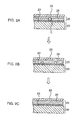
- FIG. 12 is a characteristic chart of a resistance value of a cobalt silicide layer (CoSi 2 layer) when formed on a gate electrode in a conventional semiconductor device;
- FIG. 13 is a microphotograph showing a surface state of a formation defect portion of a cobalt silicide layer formed in a polycrystalline silicon film.
- FIG. 14 is a microphotograph showing a surface state of a cobalt silicide layer formed in a polycrystalline silicon film.
- a gate electrode made smaller in width in response to the demand for miniaturization of a semiconductor device causes a so-called “thin wire effect” problem in which the resistance value of a silicide layer to be formed on the gate electrode increases, which effect is particularly prominent on an N-type gate electrode.
- the silicide layer formed on the gate electrode made of polycrystalline silicon film has many unreacted portions of silicon.
- FIG. 13 is a cross-sectional view of a cobalt silicide layer formed in the polycrystalline silicon film. This drawing shows that the size of an unreacted portion of silicon existing in the cobalt silicide layer is about 0.1 ⁇ m.
- the above-described unreacted portions of silicon uniformly exist in the silicide layer in a conventional gate electrode, and these unreacted portions of silicon cause a local break in wire in a gate electrode made smaller in width. Accordingly, when a cobalt silicide layer is formed on the gate electrode, the cobalt silicide layer increases in resistance value when the width of the gate electrode is about 0.1 ⁇ m or less as shown in FIG. 12 .
- FIG. 14 is a cross-sectional view of a formation state of a cobalt silicide layer formed in a polycrystalline silicon film examined under a transmission electron microscope (TEM).
- TEM transmission electron microscope
- silicidization of a polycrystalline silicon film makes the problems more complicated because of occurrence of unreacted portions of silicon in a silicide layer and formation of excess silicide layer.
- the inventor of the present invention devised a semiconductor device with a gate electrode composed of two-layer structure polycrystalline silicon films which are different in crystal state, for example, crystal face orientation and crystal particle diameter, as means for restraining occurrence of unreacted portions of silicon and formation of excess silicide layer.
- FIG. 1 shows a schematic diagram of a semiconductor device for explaining the outline of the present invention.
- This semiconductor device includes a gate electrode having a two-layer structure composed of a first polycrystalline silicon film 22 which is formed above a semiconductor substrate 1 with a gate insulation film 5 intervening therebetween and a second polycrystalline silicon film 25 which is formed thereabove with a separation layer 23 intervening therebetween and is different in crystal state such as crystal face orientation, crystal particle diameter, and so on from the first polycrystalline silicon film 22 .
- the second polycrystalline silicon film 25 which has a predetermined crystal face orientation directed with respect to and is smaller in crystal diameter than the first polycrystalline silicon film 22 , is formed above the first polycrystalline silicon film 22 as described above. Even if there locally exist portions having different silicidization speeds in forming a silicide layer, the above configuration makes it possible to delay the reaction with the first polycrystalline silicon film 22 and allow the silicidization reaction with unreacted portions of the second polycrystalline silicon film. Thereby, a silicide layer can be formed which is reduced in occurrence of unreacted portions of silicon and protrusions and depressions.
- the second polycrystalline silicon film 25 in which the silicide layer is to be formed was improved in film quality, and as a result, it was devised that a polycrystalline silicon film is required which has a crystal face orientation with a small mismatch in lattice constant with the silicide layer.
- the silicide layer is a cobalt silicide layer
- the polycrystalline silicon film in particular, has a silicon crystal face orientation (111) with a lattice constant of 31.83 nm, which is a small mismatch with the cobalt silicide crystal face orientation (111) with a lattice constant of 30.80 nm, so that an excellent cobalt silicide can be formed.
- the result is that the silicon crystal face orientation (111) is more easily directed in a polycrystalline silicon film formed by crystallizing an amorphous silicon film than in an ordinal polycrystalline silicon film. Then, in such a second polycrystalline silicon film 25 in which the silicon crystal face orientation (111) is directed, the silicidization reaction is accelerated to make less unreacting silicon. As a result, as shown in the resistance value characteristics in FIG. 3B , a cobalt silicide layer can be formed which is lower in resistance than that of the ordinal polycrystalline silicon film.
- This separation film 23 includes, for example, an oxide film layer which is formed very thin to a film thickness of about 0.2 nm to about 1.0 nm by a chemical treatment using hydrochloric acid or the like.
- This separation layer 23 enables prevention of growth of the second polycrystalline silicon film 25 with the first polycrystalline silicon film 22 as a core during formation of the second polycrystalline silicon film 25 by the CVD method.
- the separation layer 23 can control the silicidization reaction of a high melting point metal.
- this oxide film can intercept the silicidization reaction with the first polycrystalline silicon film 22 because a cobalt atom itself has no function of reducing the oxide film, so that the silicide layer can be formed only in the second polycrystalline silicon film 25 .
- the thickness of the silicide layer to be formed can be controlled by the film thickness of the second polycrystalline silicon film 25 .
- FIGS. 2A to 2 C show silicidization reaction processes when a high melting point metal is deposited on the semiconductor device shown in FIG. 1 .
- the following description will be made on an example using cobalt as a high melting point metal for forming a silicide layer.
- the silicidization reaction proceeds, and the cobalt silicide layer 26 is formed to reach the separation layer 23 at a plurality of portions.
- the cobalt silicide layer 26 is not formed in the first polycrystalline silicon film 22 because it is intercepted by the separation layer 23 , but the cobalt silicide layer 26 is formed at unreacted portions of the second polycrystalline silicon film 25 .
- “SEMICONDUCTOR DEVICE AND ITS MANUFACTURE” in Japanese Patent Laid-open No. Hei 10-209296 discloses ‘a gate electrode in a two-layered film structure composed of a lower layer polycrystalline silicon film and an upper layer amorphous silicon film.’
- the present invention proposes a gate electrode in a two-layered film structure composed of a first polycrystalline silicon film and a second polycrystalline silicon film thereabove which is different in crystal state from the first polycrystalline silicon film.
- the present invention is different from the above disclosure in that an upper layer is composed of a polycrystalline silicon film.
- “MANUFACTURE OF SEMICONDUCTOR DEVICE” in Japanese Patent Laid-open No. Hei 7-37992 discloses ‘a step of forming an amorphous silicon layer on a semiconductor substrate where an element isolation region and a gate insulating film are formed, . . . , a step of changing the amorphous silicon layer to a polycrystalline silicon layers by heat treatment, and a step of forming a metal silicide layer on the polycrystalline silicon layer, and thereafter, . . .
- the present invention differs therefrom in that a first polycrystalline silicon film is formed on a gate insulation film, and thereafter an amorphous silicon film is deposited and crystallized by heat treatment to form a second polycrystalline silicon film so as to form a gate electrode in the two-layer structure.
- control of the silicidization reaction is an invention for none but for a two-layer structure, which is clearly different from the gate electrode in a single layer structure described in Japanese Patent Laid-open No. Hei 7-37992.
- This embodiment discloses a CMOS transistor as a semiconductor device.
- FIG. 4 is a schematic diagram of the CMOS transistor in the embodiment of the present invention.
- the CMOS transistor of this embodiment includes, as shown in FIG. 4 , a semiconductor substrate 1 made of silicon (Si); STIs (Shallow Trench Isolations) 2 which define element active regions of an NMOS transistor 100 and a PMOS transistor 200 ; a P-type well 3 formed in a region where the NMOS transistor 100 is fabricated; a N-type well 4 formed in a region where the PMOS transistor 200 is fabricated; gate insulation films 5 formed on the semiconductor substrate 1 ; gate electrodes 6 in predetermined shapes formed on the gate insulation films 5 ; side walls 7 as protective films formed on sides walls of the gate electrodes 6 ; a source 8 and a drain 9 formed in a surface layer of the semiconductor substrate 1 within the region where the NMOS transistor 100 is fabricated; a source 10 and a drain 11 formed in the surface layer of the semiconductor substrate 1 within the region where the PMOS transistor 200 is fabricated; an interlayer insulation film 12 which electrically isolates respective wire layers; and tungsten plugs 13 embedded in contact holes in the interlayer insulation film
- the gate electrode 6 is formed of a first polycrystalline silicon film 22 , a chemical oxide film (separation layer) 23 formed very thin and uniform on the first polycrystalline silicon film 22 , and a second polycrystalline silicon film 25 which is formed on the chemical oxide film 23 and is formed therein with a cobalt silicide layer (CoSi 2 layer) layer 26 .
- all the second polycrystalline silicon film 25 may be the cobalt silicide layer 26 .
- the second polycrystalline silicon film 25 is formed to have more silicon crystal face orientation (111), which is a good match with the cobalt silicide layer, and a smaller crystal particle diameter than the first polycrystalline silicon film 22 .
- formed second polycrystalline silicon film 25 enables formation of a good quality cobalt silicide layer 26 with decreased unreacted portions of silicon.
- the silicide formation speed is locally different, it is possible to accelerate the silicidization reaction with the unreacted portions of the second polycrystalline silicon film 25 to be faster than the silicidization reaction with the first polycrystalline silicon film 22 , resulting in reduced protrusions and depressions on the interface between the cobalt silicide layer and the polycrystalline silicon film.
- the chemical oxide film 23 is formed as a separation layer for separating the second polycrystalline silicon film 25 from the first polycrystalline silicon film 22 . Even when the reaction speed of the silicidization reaction occurred between the second polycrystalline silicon film 25 and cobalt is locally different, this chemical oxide film 23 can block silicidization reaction between cobalt and the first polycrystalline silicon film 22 to conduct a control for a uniform formation of a silicide layer.
- cobalt silicide layers 8 b , 9 b , 10 b , and 11 b are formed in surfaces of the source 8 and the drain 9 of the NMOS transistor 100 and the source 10 and the drain 11 of the PMOS transistor 200 , respectively.
- the CMOS transistor of this embodiment is formed in a silicide (Self Align Silicide) structure.
- FIGS. 5A to 5 D to FIGS. 7A to 7 D are schematic cross-sectional views showing in the order of steps the first method for manufacturing the CMOS transistor in FIG. 4 .
- STIs Shallow Trench Isolations 2 are formed in a semiconductor substrate 1 made of silicon (Si) to define element active regions. Thereafter, for example, boron (B) is implanted into a region where an NMOS transistor 100 is to be fabricated to form a P-type well 3 , and for example, arsenic (As) is implanted into a region where a PMOS transistor 200 is to be fabricated to form an N-type well 4 .
- boron B
- As arsenic
- the surface of the semiconductor substrate 1 is heated at a high temperature under a temperature condition of 850° C. to 1050° C. to form a silicon oxide film (SiO 2 film) 21 with a film thickness of 5 nm to 10 nm.
- a first polycrystalline silicon film 22 is formed with a film thickness of 100 nm to 200 nm by the CVD method.
- a chemical treatment with a hydrogen peroxide solution or the like is performed to form a chemical oxide film 23 with a film thickness of 0.2 nm to 1.0 nm on the first polycrystalline silicon film 22 .
- the chemical oxide film 23 formed by the chemical treatment can be a very thin film with a uniform film thickness without addition of heat.
- an amorphous silicon film 24 is deposited to a film thickness of 5 nm to 50 nm by the CVD method.
- a resist pattern 31 is formed on the amorphous silicon film 24 by photolithography, and dry etching is performed with the resist pattern 31 as a mask to form the amorphous silicon films 24 , the chemical oxide films 23 and the first polycrystalline silicon films 22 , and gate insulation films 5 made of the silicon oxide films 21 , in predetermined shapes.
- a silicon oxide film (TEOS) 27 is deposited to a film thickness of 100 nm to 200 nm on the entire face by the CVD method.
- the entire face of the silicon oxide film 27 is anisotropically etched (etched back) by reactive ion etching (RIE) or the like to remain only on both side faces of the amorphous silicon films 24 , the chemical oxide films 23 , the first polycrystalline silicon films 22 , and the silicon oxide films 21 to form sides walls 7 .
- RIE reactive ion etching
- a resist pattern 32 which masks the region where the PMOS transistor 200 is to be fabricated, is formed by photolithography, and arsenic (As) is ion implanted into the entire face thereof under conditions of an acceleration energy of 2 keV to 15 keV, an inclination angle from the vertical direction to the surface of the semiconductor substrate 1 of about 0°, a dose amount of 1 ⁇ 10 14 /cm 2 to 8 ⁇ 10 14 /cm 2 to form N-type diffusion layers 8 a and 9 a.
- Ars arsenic
- a resist pattern 33 which masks the region where the NMOS transistor 100 is to be fabricated, is formed by photolithography, and phosphorus (P) is ion implanted into the entire face thereof under conditions of an acceleration energy of 15 keV to 25 keV, an inclination angle of about 0°, a dose amount of 2 ⁇ 10 13 /cm 2 to 8 ⁇ 10 14 /cm 2 to form P-type diffusion layers 10 a and 11 a.
- the resist pattern 33 is removed by ashing using O 2 plasma or the like. Thereafter, as shown in FIG. 7A , annealing is performed for 10 seconds at a temperature of 950° C. to 1050° C. for the surface of the semiconductor substrate 1 to activate the ion implanted impurities as well as to crystallize amorphous silicon films 24 to form second polycrystalline silicon films 25 different in crystal particle diameter and orientation from the first polycrystalline silicon films 22 .
- a cobalt thin film (Co thin film) 28 being a high melting point metal film is deposited on the entire face to a film thickness of 5 nm to 15 nm by a sputtering method. Further, a not shown titanium nitride film (TiN) as a cap layer is also deposited in this event.
- cobalt silicide layers 8 b , 9 b , 10 b , 11 b , and 26 are formed by two-step annealing in a self-alignment manner.
- annealing is performed for 30 seconds at a temperature of 520° C.
- annealing is performed for 30 seconds at a temperature of 840° C. as a second annealing.
- This forms gate electrodes 6 composed of the first polycrystalline silicon films 22 , the chemical oxide films 23 , the second polycrystalline silicon films 25 having the cobalt silicide layers 26 on upper faces thereof.
- the source 8 having the N-type diffusion layer 8 a with the cobalt silicide layer 8 b provided thereon and the drain 9 having the N-type diffusion layer 9 a with the cobalt silicide layer 9 b provided thereon are formed in the region where the NMOS transistor 100 is fabricated.
- the source 10 having the P-type diffusion layer 10 a with the cobalt silicide layer 10 b provided thereon and the drain 11 having the P-type diffusion layer 11 a with the cobalt silicide layer 11 b provided thereon, are formed in the region where the PMOS transistor 200 is fabricated.
- an interlayer insulation film 12 is deposited by the CVD method, and contact holes for lead electrodes are formed in the interlayer insulation film 12 by dry etching. Then, tungsten (W) is deposited on the entire face by the CVD method, and thereafter its surface is polished by CMP to form tungsten plugs 13 embedded in the contact holes.
- CMOS transistor of this embodiment Thereafter, lead electrodes to be connected to the tungsten plugs 13 are formed, and then a surface protective film (passivation protective film) for protecting the device is further formed, thus completing the CMOS transistor of this embodiment.
- annealing is performed for 10 seconds at a temperature of 950° C. to 1050° C. for the surface of a semiconductor substrate 1 to crystallize the amorphous silicon film 24 to form the second polycrystalline silicon film 25 different in crystal particle diameter and orientation from a first polycrystalline silicon film 22 .
- a resist pattern 31 is formed on the second polycrystalline silicon film 25 by photolithography, and dry etching is performed with the resist pattern 31 as a mask to form the second polycrystalline silicon films 25 , chemical oxide films 23 , the first polycrystalline silicon films 22 , and gate insulation films 5 made of silicon oxide films 21 , in predetermined shapes.
- a silicon oxide film (TEOS) 27 is deposited to a film thickness of 100 nm to 200 nm on the entire face by the CVD method.
- the entire face of the silicon oxide film 27 is anisotropically etched (etched back) by reactive ion etching (RIE) or the like to remain only on both side faces of the second polycrystalline silicon films 25 , the chemical oxide films 23 , the first polycrystalline silicon films 22 , and the silicon oxide films 21 to form sides walls 7 .
- RIE reactive ion etching
- a resist pattern 32 which masks a region where a PMOS transistor 200 is to be fabricated, is formed by photolithography, and arsenic (As) is ion implanted into the entire face thereof under conditions of an acceleration energy of 2 keV to 15 keV, an inclination angle of about 0°, a dose amount of 1 ⁇ 10 14 /cm 2 to 8 ⁇ 10 14 /cm 2 to form N-type diffusion layers 8 a and 9 a.
- Ars arsenic
- a resist pattern 33 which masks a region where an NMOS transistor 100 is to be fabricated, is formed by photolithography, and phosphorus (P) is ion implanted into the entire face thereof under conditions of an acceleration energy of 15 keV to 25 keV, an inclination angle of about 0°, a dose amount of 2 ⁇ 10 13 /cm 2 to 8 ⁇ 10 14 /cm 2 to form P-type diffusion layers 10 a and 11 a.
- the resist pattern 33 is removed by ashing using O 2 plasma or the like. Thereafter, as shown in FIG. 9C , annealing is performed for 10 seconds at a temperature of 950° C. to 1050° C. for the surface of the semiconductor substrate 1 to activate the ion implanted impurities.
- CMOS transistor of this embodiment Thereafter, lead electrodes to be connected to tungsten plugs 13 are formed, and then a surface protective film (passivation protective film) for protecting the device is further formed, thus completing the CMOS transistor of this embodiment.
- the device using cobalt silicide as a high melting point metal silicide is disclosed in this embodiment, but the present invention is not limited to this.
- titanium silicide, nickel silicide, and platinum silicide are also applicable.
- the film thickness of the second polycrystalline silicon film 25 is made no more than 3.5 times the thickness of cobalt silicide, no more than 2.5 times the thickness of titanium silicide, no more than 3.6 times the thickness of nickel silicide, or no more than 2.0 times the thickness of platinum silicide, the film thickness of silicide to be formed can be controlled by the film thickness of the second polycrystalline silicon film 25 .
- the device using the chemical oxide film 23 as a separation layer which is formed for varying the second polycrystalline silicon film 25 from the first polycrystalline silicon film 22 in crystal face orientation and crystal particle diameter, is disclosed in this embodiment, but the present invention is not limited to this.
- a separation layer is applicable as long as it is formed of a material other than the polycrystalline silicon film and satisfies the above-described main function, and may be composed of a conductor or the like.
- FIG. 10 is surface views of cobalt silicide layers formed in gate electrodes in the CMOS transistors of this embodiment. For comparison, a surface view in a case of a single-layer polycrystalline silicon film is also shown.
- FIG. 10 verifies that while there exist formation defects due to unreacting silicon in the silicide layer in the case of the single-layer polycrystalline silicon film, such a formation defect is not recognized in the CMOS transistors of this embodiment having two-layer polycrystalline silicon films in which excellent silicide layers can be formed.
- FIG. 11 is a characteristic chart of a resistance value of the cobalt silicide layer formed in the gate electrode in the CMOS transistor of this embodiment.
- the conventional CMOS transistor sharply rises in resistance value to 10 ⁇ or more per unit area, while the CMOS transistor of this embodiment rises to 6 ⁇ or less per unit area. It was verified that line width dependence, that is, a thin wire effect of the resistance value of the silicide layer can be suppressed.
- the silicidization reaction can be controlled by the film thickness of the second polycrystalline silicon film 25 from the fact that changes were recognized in the resistance values of the silicide layers (25 nm and 35 nm) depending on the film thickness of the second polycrystalline silicon film 25 .
- a silicide layer can be formed excellent and uniform in a gate electrode to enable realization of a highly reliable semiconductor device and a method for manufacturing the same which restrain the increase in resistance value of a gate electrode caused by a thin wire effect, decrease resistance variations of the gate electrode, and prevent deterioration of the gate electrode.
Landscapes
- Electrodes Of Semiconductors (AREA)
- Insulated Gate Type Field-Effect Transistor (AREA)
- Metal-Oxide And Bipolar Metal-Oxide Semiconductor Integrated Circuits (AREA)
Abstract
Description
Claims (28)
Applications Claiming Priority (2)
| Application Number | Priority Date | Filing Date | Title |
|---|---|---|---|
| JP2002-273624 | 2002-09-19 | ||
| JP2002273624A JP2004111736A (en) | 2002-09-19 | 2002-09-19 | Semiconductor device and manufacturing method thereof |
Publications (2)
| Publication Number | Publication Date |
|---|---|
| US20040089902A1 US20040089902A1 (en) | 2004-05-13 |
| US6873022B2 true US6873022B2 (en) | 2005-03-29 |
Family
ID=32211512
Family Applications (1)
| Application Number | Title | Priority Date | Filing Date |
|---|---|---|---|
| US10/662,810 Expired - Lifetime US6873022B2 (en) | 2002-09-19 | 2003-09-16 | Semiconductor device and method for manufacturing the same |
Country Status (5)
| Country | Link |
|---|---|
| US (1) | US6873022B2 (en) |
| JP (1) | JP2004111736A (en) |
| KR (1) | KR101051987B1 (en) |
| CN (1) | CN1262010C (en) |
| TW (1) | TWI240961B (en) |
Families Citing this family (6)
| Publication number | Priority date | Publication date | Assignee | Title |
|---|---|---|---|---|
| US20050277237A1 (en) * | 2004-06-14 | 2005-12-15 | Mei-Yun Wang | Structure from which an integrated circuit may be fabricated and a method of making same |
| US7939396B2 (en) * | 2006-06-09 | 2011-05-10 | Taiwan Semiconductor Manufacturing Company, Ltd. | Base oxide engineering for high-K gate stacks |
| CN101295730B (en) * | 2007-04-24 | 2010-05-19 | 中芯国际集成电路制造(上海)有限公司 | Semiconductor device and its grid production method |
| US20100052077A1 (en) * | 2008-08-27 | 2010-03-04 | Taiwan Semiconductor Manufacturing Company, Ltd. | High-k metal gate structure including buffer layer |
| KR20100074638A (en) * | 2008-12-24 | 2010-07-02 | 주식회사 하이닉스반도체 | Gate pattern of semiconductor device and forming method of the same |
| CN104124209B (en) * | 2013-04-27 | 2017-02-15 | 上海华虹宏力半导体制造有限公司 | CMOS device manufacturing method |
Citations (1)
| Publication number | Priority date | Publication date | Assignee | Title |
|---|---|---|---|---|
| US5903053A (en) * | 1994-02-21 | 1999-05-11 | Kabushiki Kaisha Toshiba | Semiconductor device |
Family Cites Families (1)
| Publication number | Priority date | Publication date | Assignee | Title |
|---|---|---|---|---|
| JP2002208645A (en) * | 2001-01-09 | 2002-07-26 | Mitsubishi Electric Corp | Nonvolatile semiconductor memory device and method of manufacturing the same |
-
2002
- 2002-09-19 JP JP2002273624A patent/JP2004111736A/en active Pending
-
2003
- 2003-09-16 US US10/662,810 patent/US6873022B2/en not_active Expired - Lifetime
- 2003-09-16 TW TW092125514A patent/TWI240961B/en active
- 2003-09-19 KR KR1020030065102A patent/KR101051987B1/en not_active Expired - Fee Related
- 2003-09-19 CN CNB031587070A patent/CN1262010C/en not_active Expired - Fee Related
Patent Citations (1)
| Publication number | Priority date | Publication date | Assignee | Title |
|---|---|---|---|---|
| US5903053A (en) * | 1994-02-21 | 1999-05-11 | Kabushiki Kaisha Toshiba | Semiconductor device |
Non-Patent Citations (2)
| Title |
|---|
| Patent Abstracts of Japan, Publication No. 10-209296, published Aug. 7, 1998./Discussed in the specification. |
| Patent Abstracts of Japan, Publication No. 7-37992, published Feb. 7, 1995./Discussed in the specification. |
Also Published As
| Publication number | Publication date |
|---|---|
| CN1262010C (en) | 2006-06-28 |
| US20040089902A1 (en) | 2004-05-13 |
| TWI240961B (en) | 2005-10-01 |
| KR20040025646A (en) | 2004-03-24 |
| TW200406830A (en) | 2004-05-01 |
| JP2004111736A (en) | 2004-04-08 |
| CN1495903A (en) | 2004-05-12 |
| KR101051987B1 (en) | 2011-07-26 |
Similar Documents
| Publication | Publication Date | Title |
|---|---|---|
| JP2891092B2 (en) | Method for manufacturing semiconductor device | |
| US20070215951A1 (en) | Semiconductor devices having silicided electrodes | |
| US8865592B2 (en) | Silicided semiconductor structure and method of forming the same | |
| US5593923A (en) | Method of fabricating semiconductor device having refractory metal silicide layer on impurity region using damage implant and single step anneal | |
| JP3545526B2 (en) | Method for manufacturing semiconductor device | |
| US5059554A (en) | Method for forming polycrystalline silicon contacts | |
| US6873022B2 (en) | Semiconductor device and method for manufacturing the same | |
| JP2891093B2 (en) | Manufacturing method of semiconductor integrated circuit | |
| JP3518122B2 (en) | Method for manufacturing semiconductor device | |
| KR100205159B1 (en) | Process of fabricating field effect transistor having reliable polycide gaye electrode | |
| JP2636786B2 (en) | Method for manufacturing semiconductor device | |
| JP3190858B2 (en) | Semiconductor device and method of manufacturing the same | |
| JPH1093077A (en) | Semiconductor device and manufacturing method thereof | |
| JPH0831931A (en) | Semiconductor device and manufacturing method thereof | |
| JP3204007B2 (en) | Method for manufacturing semiconductor device | |
| JP2819918B2 (en) | Method for manufacturing semiconductor integrated circuit device | |
| JP3263155B2 (en) | Method of manufacturing electrode and method of manufacturing semiconductor device using the same | |
| KR100518220B1 (en) | Method for forming bit line of semiconductor device | |
| JP2000156356A (en) | Method for manufacturing semiconductor device | |
| KR100318273B1 (en) | Method for forming bit line of semiconductor device | |
| JPH11261071A (en) | Gate electrode and method of manufacturing the same | |
| KR100318260B1 (en) | Manufacturing method of semiconductor device | |
| KR20000041468A (en) | Method of forming polycide gate electrode by using silicon film of amorphous phase | |
| KR20010016657A (en) | Method for forming ohmic contact on semiconductor device | |
| JPH09293722A (en) | Method for manufacturing semiconductor device |
Legal Events
| Date | Code | Title | Description |
|---|---|---|---|
| AS | Assignment |
Owner name: FASL LLC, CALIFORNIA Free format text: ASSIGNMENT OF ASSIGNORS INTEREST;ASSIGNOR:HAYAKAWA, YUKIO;REEL/FRAME:014819/0559 Effective date: 20030919 |
|
| AS | Assignment |
Owner name: FASL LLC, CALIFORNIA Free format text: ASSIGNMENT OF ASSIGNORS INTEREST;ASSIGNOR:HAYAKAWA, YUKIO;REEL/FRAME:015536/0001 Effective date: 20030919 |
|
| STCF | Information on status: patent grant |
Free format text: PATENTED CASE |
|
| AS | Assignment |
Owner name: SPANSION LLC, CALIFORNIA Free format text: CHANGE OF NAME;ASSIGNOR:FASL LLC;REEL/FRAME:019084/0842 Effective date: 20070111 |
|
| FPAY | Fee payment |
Year of fee payment: 4 |
|
| AS | Assignment |
Owner name: BARCLAYS BANK PLC,NEW YORK Free format text: SECURITY AGREEMENT;ASSIGNORS:SPANSION LLC;SPANSION INC.;SPANSION TECHNOLOGY INC.;AND OTHERS;REEL/FRAME:024522/0338 Effective date: 20100510 Owner name: BARCLAYS BANK PLC, NEW YORK Free format text: SECURITY AGREEMENT;ASSIGNORS:SPANSION LLC;SPANSION INC.;SPANSION TECHNOLOGY INC.;AND OTHERS;REEL/FRAME:024522/0338 Effective date: 20100510 |
|
| FPAY | Fee payment |
Year of fee payment: 8 |
|
| AS | Assignment |
Owner name: SPANSION LLC, CALIFORNIA Free format text: RELEASE BY SECURED PARTY;ASSIGNOR:BARCLAYS BANK PLC;REEL/FRAME:035201/0159 Effective date: 20150312 Owner name: SPANSION INC., CALIFORNIA Free format text: RELEASE BY SECURED PARTY;ASSIGNOR:BARCLAYS BANK PLC;REEL/FRAME:035201/0159 Effective date: 20150312 Owner name: SPANSION TECHNOLOGY LLC, CALIFORNIA Free format text: RELEASE BY SECURED PARTY;ASSIGNOR:BARCLAYS BANK PLC;REEL/FRAME:035201/0159 Effective date: 20150312 |
|
| AS | Assignment |
Owner name: MORGAN STANLEY SENIOR FUNDING, INC., NEW YORK Free format text: SECURITY INTEREST;ASSIGNORS:CYPRESS SEMICONDUCTOR CORPORATION;SPANSION LLC;REEL/FRAME:035240/0429 Effective date: 20150312 |
|
| AS | Assignment |
Owner name: CYPRESS SEMICONDUCTOR CORPORATION, CALIFORNIA Free format text: ASSIGNMENT OF ASSIGNORS INTEREST;ASSIGNOR:SPANSION, LLC;REEL/FRAME:036036/0001 Effective date: 20150601 |
|
| FPAY | Fee payment |
Year of fee payment: 12 |
|
| AS | Assignment |
Owner name: MONTEREY RESEARCH, LLC, CALIFORNIA Free format text: ASSIGNMENT OF ASSIGNORS INTEREST;ASSIGNOR:CYPRESS SEMICONDUCTOR CORPORATION;REEL/FRAME:044938/0360 Effective date: 20171218 |
|
| AS | Assignment |
Owner name: CYPRESS SEMICONDUCTOR CORPORATION, CALIFORNIA Free format text: RELEASE BY SECURED PARTY;ASSIGNOR:MORGAN STANLEY SENIOR FUNDING, INC;REEL/FRAME:044949/0962 Effective date: 20171218 Owner name: SPANSION LLC, CALIFORNIA Free format text: RELEASE BY SECURED PARTY;ASSIGNOR:MORGAN STANLEY SENIOR FUNDING, INC;REEL/FRAME:044949/0962 Effective date: 20171218 |
|
| AS | Assignment |
Owner name: MORGAN STANLEY SENIOR FUNDING, INC., NEW YORK Free format text: CORRECTIVE ASSIGNMENT TO CORRECT THE 8647899 PREVIOUSLY RECORDED ON REEL 035240 FRAME 0429. ASSIGNOR(S) HEREBY CONFIRMS THE SECURITY INTERST;ASSIGNORS:CYPRESS SEMICONDUCTOR CORPORATION;SPANSION LLC;REEL/FRAME:058002/0470 Effective date: 20150312 |