US6854041B2 - DRAM-based separate I/O memory solution for communication applications - Google Patents
DRAM-based separate I/O memory solution for communication applications Download PDFInfo
- Publication number
- US6854041B2 US6854041B2 US10/065,839 US6583902A US6854041B2 US 6854041 B2 US6854041 B2 US 6854041B2 US 6583902 A US6583902 A US 6583902A US 6854041 B2 US6854041 B2 US 6854041B2
- Authority
- US
- United States
- Prior art keywords
- bank
- read
- write
- during
- cycle
- Prior art date
- Legal status (The legal status is an assumption and is not a legal conclusion. Google has not performed a legal analysis and makes no representation as to the accuracy of the status listed.)
- Expired - Lifetime, expires
Links
Images


Classifications
-
- G—PHYSICS
- G11—INFORMATION STORAGE
- G11C—STATIC STORES
- G11C11/00—Digital stores characterised by the use of particular electric or magnetic storage elements; Storage elements therefor
- G11C11/21—Digital stores characterised by the use of particular electric or magnetic storage elements; Storage elements therefor using electric elements
- G11C11/34—Digital stores characterised by the use of particular electric or magnetic storage elements; Storage elements therefor using electric elements using semiconductor devices
- G11C11/40—Digital stores characterised by the use of particular electric or magnetic storage elements; Storage elements therefor using electric elements using semiconductor devices using transistors
- G11C11/401—Digital stores characterised by the use of particular electric or magnetic storage elements; Storage elements therefor using electric elements using semiconductor devices using transistors forming cells needing refreshing or charge regeneration, i.e. dynamic cells
- G11C11/406—Management or control of the refreshing or charge-regeneration cycles
- G11C11/40618—Refresh operations over multiple banks or interleaving
-
- G—PHYSICS
- G11—INFORMATION STORAGE
- G11C—STATIC STORES
- G11C11/00—Digital stores characterised by the use of particular electric or magnetic storage elements; Storage elements therefor
- G11C11/21—Digital stores characterised by the use of particular electric or magnetic storage elements; Storage elements therefor using electric elements
- G11C11/34—Digital stores characterised by the use of particular electric or magnetic storage elements; Storage elements therefor using electric elements using semiconductor devices
- G11C11/40—Digital stores characterised by the use of particular electric or magnetic storage elements; Storage elements therefor using electric elements using semiconductor devices using transistors
- G11C11/401—Digital stores characterised by the use of particular electric or magnetic storage elements; Storage elements therefor using electric elements using semiconductor devices using transistors forming cells needing refreshing or charge regeneration, i.e. dynamic cells
- G11C11/406—Management or control of the refreshing or charge-regeneration cycles
-
- G—PHYSICS
- G11—INFORMATION STORAGE
- G11C—STATIC STORES
- G11C11/00—Digital stores characterised by the use of particular electric or magnetic storage elements; Storage elements therefor
- G11C11/21—Digital stores characterised by the use of particular electric or magnetic storage elements; Storage elements therefor using electric elements
- G11C11/34—Digital stores characterised by the use of particular electric or magnetic storage elements; Storage elements therefor using electric elements using semiconductor devices
- G11C11/40—Digital stores characterised by the use of particular electric or magnetic storage elements; Storage elements therefor using electric elements using semiconductor devices using transistors
- G11C11/401—Digital stores characterised by the use of particular electric or magnetic storage elements; Storage elements therefor using electric elements using semiconductor devices using transistors forming cells needing refreshing or charge regeneration, i.e. dynamic cells
- G11C11/4063—Auxiliary circuits, e.g. for addressing, decoding, driving, writing, sensing or timing
- G11C11/407—Auxiliary circuits, e.g. for addressing, decoding, driving, writing, sensing or timing for memory cells of the field-effect type
- G11C11/409—Read-write [R-W] circuits
-
- G—PHYSICS
- G11—INFORMATION STORAGE
- G11C—STATIC STORES
- G11C7/00—Arrangements for writing information into, or reading information out from, a digital store
- G11C7/10—Input/output [I/O] data interface arrangements, e.g. I/O data control circuits, I/O data buffers
- G11C7/1015—Read-write modes for single port memories, i.e. having either a random port or a serial port
- G11C7/1042—Read-write modes for single port memories, i.e. having either a random port or a serial port using interleaving techniques, i.e. read-write of one part of the memory while preparing another part
-
- G—PHYSICS
- G11—INFORMATION STORAGE
- G11C—STATIC STORES
- G11C7/00—Arrangements for writing information into, or reading information out from, a digital store
- G11C7/22—Read-write [R-W] timing or clocking circuits; Read-write [R-W] control signal generators or management
Definitions
- the present invention generally relates to integrated circuits and, more particularly to input/output (I/O) architecture, and read/write systems for high bandwidth semiconductor memories.
- I/O input/output
- DRAMs dynamic random access memories
- EDO extended data output
- SDRAMs synchronous DRAMs
- this increase in bandwidth is often accompanied by a significant increase in the overall size and cost of the memory device.
- one of the drawbacks of conventional QDR SRAMs is the corresponding increase in the overall size, and specifically, the number of I/O interconnect lines required to process the quad bits during read and write operations.
- a 4-bit pre-fetch results in 4N bits of data being output from the memory array in read mode.
- the total columns in an array are divided into two sets of even and odd columns, each delivering N bits of data.
- the 2N columns connect to corresponding 2N sense amplifiers, with the 2N sense amplifiers driving 2N global I/O lines.
- FIG. 1 shows a conventional SRAM QDR timing diagram with an 8 ns cycle, and a burst of 4.
- conventional DRAM banking solutions use any number of banks to improve cycle time and data rate by:
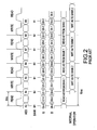
- FIG. 2 illustrates a conventional two-bank DRAM QDR timing diagram with an 8 ns cycle, and a burst of 4.
- banking protocols exist which partition the memory array into several different arrays, which can then be independently addressable. That is, the partition of the memory array occurs in the bank.
- FIG. 1 in an 8 ns timing protocol, a first bank (Bank 1 ) is accessed. After an 8 ns cycle lapses, only then can the same bank (Bank 1 ) be accessed.
- the same bank may be accessed only every 8 ns (the length of the entire cycle time), and during the cycle, only other banks may be accessed, not the same bank.
- bandwidth maximization is achieved; as such data throughput is maximized.
- the disadvantage of such multi-banking approaches is it breaks away from the desired randomness, which is sought in banking address operations. Therefore, there is a need to access the same bank back-to-back using a multi-bank approach.
- the invention provides a DRAM-based separate I/O memory solution for communication applications.
- the present invention provides a DRAM-based solution to the standard QDR communications-SRAM solution.
- the present invention provides data rate and cycle times comparable to conventional QDR SRAMs.
- the present invention achieves at least four times the density and price/bit of conventional QDR SRAM implementations.
- the present invention provides a novel banking system allowing back-to-back operations to be performed on a given bank.
- a method of performing back-to back read and write memory operations to the same DRAM bank comprises articulating between reading data on a first bank during successive first bank read cycles and writing data to a second bank during successive second bank write cycles, cycling between reading data on the second bank during successive second bank read cycles and writing data to the first bank during successive first bank write cycles, and performing a refresh cycle on the first and second bank, wherein the first bank write cycles lag the first bank read cycles, and wherein the second bank write cycles lag the second bank read cycles.
- the step of articulating comprises reading data on the first bank during the first bank read cycle, writing data to the second bank during the second bank write cycle, reading additional data on the first bank during the first bank read cycle, and writing additional data to the second bank during the second bank write cycle.
- the step of cycling comprises reading data on the second bank during the second bank read cycle, writing data to the first bank during the first bank write cycle, reading additional data on the second bank during the second bank read cycle, and writing additional data to the first bank during the first bank write cycle.
- a refresh cycle is performed on the first bank after the step of writing additional data to the second bank. Additionally, a refresh cycle is performed on the second bank after the step of writing additional data to the first bank.
- the read/write memory operations constantly swap between the read and write cycles. Moreover, the read/write memory operations constantly swap between the first and second bank. Also, the read/write memory operations occur in a frequency of 2n times within the same bank. Furthermore, the lag comprises at least two write cycles.
- the present invention also provides a method of performing back-to-back read/write memory operations to a same DRAM bank, wherein the method comprises reading data on a first bank during an nth read cycle, writing data to a second bank during a nth write cycle, reading data on the first bank during a (nth+1) read cycle, writing data to the second bank during a (nth+1) write cycle, refreshing data on the first bank, reading data on the second bank during a (nth+2) read cycle, writing data to the first bank during a (nth+2) write cycle, reading data on the second bank during a (nth+3) read cycle, writing data to the first bank during a (nth+3) write cycle, and refreshing data on the second bank, wherein the read/write memory operations occur in a frequency of 2n times within the same bank.
- a method of accessing banks of dynamic random access memory (DRAM) memory comprises applying a first group of access requests to a first DRAM memory bank during a first time period, wherein at least one of the access requests is buffered; and applying a second group of access requests to a second DRAM memory bank during a second time period, wherein access requests that are buffered during the first time period are executed during the second time period.
- the first and second group of access requests comprise read/write memory operations constantly swapping between read and write cycles, wherein the read/write memory operations occur in a frequency of 2n times within each of the first DRAM memory bank and the second DRAM memory bank, respectively.
- the present invention further comprises a multi-bank memory circuit operable to allow back-to-back read/write memory operations to be performed on a same DRAM bank, wherein the circuit comprises a plurality of independently addressable DRAM memory banks, a refresh counter connected to the DRAM memory banks, a read register connected to the DRAM memory banks, a write register connected to the DRAM memory banks, and an address comparator connected to the read and write registers, wherein the refresh counter is operable to send an address to each DRAM memory bank, wherein the read register is operable to send a read address to each DRAM memory bank, wherein the write register is operable to send a write address to each DRAM memory bank, and wherein the address comparator is operable to compare the read and write addresses.
- the circuit further comprises a partition array located in each DRAM memory bank, and an input clock operatively connected to the read and write registers, wherein the input clock is operable to capture the data from the read and write registers.
- the address comparator monitors the write registers to determine if the write address has been stored in the partition array.
- the refresh counter is operable to track all addresses to be refreshed.
- the read/write memory operations constantly swap between a read and write cycle.
- the plurality of DRAM memory banks comprises a first and second DRAM memory bank, wherein the read/write memory operations constantly swap between the first and second DRAM memory banks. Furthermore, the read/write memory operations occur in a frequency of 2n times within the same bank.
- the present invention provides a novel DRAM-based separate I/O memory solution for communication applications. Also, the present invention provides a novel DRAM-based solution to the standard QDR communications-SRAM solution. Additionally, the present invention provides data rate and cycle times comparable to conventional QDR SRAMs. Furthermore, the present invention achieves at least four times the density and price/bit of conventional QDR SRAM implementations. Another benefit of the present invention is that it provides a novel banking system whereby back-to-back operations are performed on a given bank.
- FIG. 1 is a schematic illustration of a conventional QDR SRAM timing diagram
- FIG. 2 is a schematic illustration of a conventional two-bank QDR DRAM timing diagram
- FIG. 3 is a schematic illustration of a QDR timing diagram according to the present invention.
- FIG. 5 is a schematic block diagram of a multi-bank memory system according to the present invention.
- FIG. 6 is a flow diagram illustrating a preferred method of the invention.
- FIG. 7 is a flow diagram illustrating a preferred method of the invention.
- FIG. 8 is a flow diagram illustrating a preferred method of the invention.
- FIG. 9 is a flow diagram illustrating a preferred method of the invention.
- FIG. 10 is a flow diagram illustrating a preferred method of the invention.
- FIG. 11 is a system diagram according to the present invention.
- FIGS. 3 through 11 there are shown preferred embodiments of the methods and structures according to the present invention.
- a DRAM solution is most useful as a replacement to QDR-SRAM if back-to-back operations can be performed on the same bank.
- the present invention solves the problems inherent in the prior art solutions.
- the multi-bank memory device of the present invention allows back-to-back read-write operations to the same bank.
- the present invention simulates a process where it appears that a refresh operation is unnecessary by using buffers to bury the refresh operations between read and write cycles. As such, the present invention provides a background refresh operation to take place between the banks, thereby burying the refresh operations as indicated above. This assures that all of the rows in the memory are adequately refreshed. During this background refresh operation, a counter counts the rows, thereby reading the rows. Thus, not all rows are refreshed during one operation as with conventional devices.
- the invention accesses memory locations through location address A 3 (the memory data must wait because of the inherent latency of DRAM as mentioned above). Then, during the next read cycle, the data comes out in a burst of 4 through address A 5 .
- the present invention holds data into output registers, while burst registers hold the data from address A 3 to A 5 .
- the present invention allows the write data to be presented to the memory two cycles after the write command. Essentially, the present invention lags the read and write cycles. As shown in FIG. 3 , during the first write cycle, 4 burst bits of data, D 2 - 0 , D 2 - 1 , D 2 - 2 , and D 2 - 3 are held in a buffer. Also, the data coming out of the memory during the first read cycle (at A 3 ), Q 0 - 1 , Q 0 - 2 , and Q 0 - 3 is read data from the previous read operation.
- FIG. 4 illustrates a detailed timing protocol diagram in a multi-bank DRAM implementation with back-to-back read/write operations to the same bank. This illustrates what occurs in the memory (internal RAM operation). For example, there are twelve cycles shown (labeled A through L). The read cycles always occur in the same cycle. Specifically, during the memory operation of Cycle A, a read operation (reading data Q 3 - 0 , Q 3 - 1 , Q 3 - 2 , and Q 3 - 3 ) for that cycle occurs (i.e., read Cycle A) on a first bank (B 1 ). However, the write operation on the first bank (B 1 ) is lagged, and does not occur until after two write cycles occur on the second bank (B 2 ).
- a read operation reading data Q 3 - 0 , Q 3 - 1 , Q 3 - 2 , and Q 3 - 3
- the write operation on the first bank (B 1 ) is lagged, and does not occur until after two write cycles occur on the second bank (
- the present invention provides a continuous internal bank swap (B 1 -B 2 flip flop).
- the CQ represents an echo clock, wherein the memory device outputs Q and CQ data signals and is received by a receiving device, such as a processor or cache, which uses the echo clock to capture the data Q.
- the refresh cycle operations are sandwiched (buried) in between two bank swaps, as further illustrated in FIG. 4 . As a result, no refresh-only operations are required.
- the DRAM-specific separate I/O timing protocol described above and illustrated in FIGS. 3 and 4 illustrate how the high bandwidth can be obtained with a DRAM-based solution.
- the latency is not as aggressive as what a SRAM counterpart offers, the DRAM approach of the present invention provides as high or higher bandwidth (data rate) with a corresponding density increase and reduction in chip size.
- the DRAM design of the present invention provides the data width necessary for the high frequency bursting of data.
- FIG. 5 illustrates a multi bank memory circuit 1 operable to allow back-to-back read/write memory operations to be performed on a same DRAM bank 3 , 5 , wherein the circuit 1 comprises a plurality of independently addressable DRAM memory banks 3 , 5 ; a refresh counter 7 connected to the DRAM memory banks 3 , 5 ; a read register 13 connected to the DRAM memory banks 3 , 5 ; a write register 15 connected to the DRAM memory banks 3 , 5 ; an address comparator 17 connected to the read and write registers 13 , 15 , respectively; and a plurality of buffers connected to the DRAM memory banks, wherein the buffers artificially reduces an apparent cycle time of the DRAM memory banks, wherein the refresh counter 7 is operable to send an address 9 , 11 to each DRAM memory bank 3 , 5 , wherein the read register 13 is operable to send a read address to each DRAM memory bank 3 , 5 , wherein the write address registers 16 are operable to send a write address to each DRAM
- the circuit 1 further comprises a partition array 19 , 21 located in each DRAM memory bank 3 , 5 , respectively, and an input clock 27 operatively connected to the read and write registers 13 , 15 , wherein the input clock 27 is operable to capture the data D, Q from the read and write registers 13 , 15 .
- the address comparator 17 monitors the write address registers 16 to determine if the write address has been stored in the partition array 19 , 21 .
- the refresh counter 7 is operable to track all addresses to be refreshed.
- the read/write memory operations constantly swap between a read and write cycle.
- the plurality of DRAM memory banks comprises a first and second DRAM memory bank 3 , 5 , respectively, wherein the read/write memory operations constantly swap between the first and second DRAM memory banks 3 , 5 , respectively.
- the read/write memory operations occur in a frequency of 2n times within the same bank 3 , 5 , again making it appear as though the cycle time is less than the actual cycle time.
- an input registering/control unit 25 is provided in the circuit 1 which connects to the input clock 27 .
- the invention achieves a number of advantages by grouping read/write access requests. While one group of access requests is being made to a first bank 3 , no access requests are made to an alternate second DRAM memory bank 5 . Once the group of access requests is completed on the first bank 3 , a second group of access requests is applied to the second alternate DRAM memory bank 5 . Thus, during a first time period, a first group of access requests is made to a first DRAM memory bank 3 and no access requests are made to a second DRAM memory bank 5 . During the next time period, a second group of access requests are made to the second DRAM memory bank 5 while no access requests are made to the first DRAM memory bank 3 .
- each DRAM memory bank 3 , 5 has some “idle time” during which no access requests are being directly made.
- the invention utilizes this “idle time” to reduce the apparent cycle time of each of the banks 3 , 5 .
- the invention accepts more requests than can be processed during each bank's cycle time and buffers half of the requests. Then, during that bank's idle time (when that bank is not receiving direct accessed requests), the buffered requests can be processed. With two banks, the apparent cycle time can be reduced in half. With four banks operating according to this system, the apparent second time can be reduced to 1 ⁇ 4 the actual cycle time.
- the invention artificially reduces the apparent cycle time of the different DRAM memory banks 3 , 5 through the use of buffers.
- the invention processes a first request (a read request) and accepts a second request (a write request) before the first bank's cycle time has completed.
- the invention stores this second request in a buffer and processes it later during its idle time.
- the invention accepts as a third request (a second read request).
- the bank's cycle time has completed so that it can process the third request.
- the second request still remains in a buffer.
- the invention can then take a fourth request (a second write request) before the cycle time has completed, so long as this request is also placed in a buffer.
- a feature of the invention is that while the invention is handling requests for the second DRAM memory bank 5 , it has time to process the buffered requests on the first bank 3 . This allows the invention to make it appear as though the cycle time is less than the actual cycle time. However, in reality, because the operations are performed in groups, half of the operations are buffered. These buffer operations are executed while requests are made to another bank.
- banks 1 and 2 ( 3 , 5 ) in FIG. 5 could have a cycle time of 10 nanoseconds.
- the invention allows back-to-back read and write requests to occur every 5 nanoseconds. For example, if there were four requests in a group, this would take 20 nanoseconds. Given the cycle time of 10 nanoseconds, two requests of the group could be directly processed and two would be buffered. The first and third requests (read requests) made to bank 1 would be executed while the second and third requests (write requests) would be buffered. Then, a second group of requests would be made to bank 2 . This second group of requests (e.g., 4 requests) also consumes 20 nanoseconds.
- bank 1 This 20 nanoseconds is used by bank 1 to process the two buffered write requests.
- bank 2 would buffer two requests which would be processed during bank 2 's idle time (during the next group of access requests made to bank 1 ).
- a method of performing back-to-back read/write memory operations to a same DRAM bank is illustrated in the flow diagram in FIG. 6 , wherein the method comprises articulating 100 between reading data on a first bank 3 during successive first bank read cycles and writing data to a second bank 5 during successive second bank write cycles, cycling 200 between reading data on the second bank 5 during successive second bank read cycles and writing data to the first bank 3 during successive first bank write cycles, and performing 300 a refresh cycle on the first and second bank 3 , 5 , respectively, wherein the first bank write cycles lag (are delayed) the first bank read cycles, and wherein the second bank write cycles lag (are delayed) the second bank read cycles.
- the lag or delay period comprises at least two write cycles.
- the step of articulating 100 comprises reading 105 data on the first bank 3 during the first bank read cycle, writing 110 data to the second bank 5 during the second bank write cycle, reading 115 additional data on the first bank 3 during the first bank read cycle, and writing 120 additional data to the second bank during the second bank write cycle.
- the step of cycling 200 comprises reading 205 data on the second bank 5 during the second bank read cycle, writing 210 data to the first bank 3 during the first bank write cycle, reading 215 additional data on the second bank 5 during the second bank read cycle, and writing 220 additional data to the first bank 3 during the first bank write cycle.
- the step 300 of performing a refresh cycle occurs on the first bank 3 after the step 120 of writing additional data to the second bank 5 . Additionally, the step 300 of performing a refresh cycle is performed on the second bank 5 after the step 220 of writing additional data to the first bank 3 .
- the present invention provides a method of performing back-to-back read/write memory operations to a same DRAM bank, wherein the method comprises reading 400 data on a first bank 3 during an nth read cycle, writing 405 data to a second bank 5 during a nth write cycle, reading 410 data on the first bank 3 during a (nth+1) read cycle, writing 415 data to the second bank 5 during a (nth+1) write cycle, refreshing 420 data on the first bank 3 , reading 425 data on the second bank 5 during a (nth+2) read cycle, writing 430 data to the first bank 3 during a (nth+2) write cycle, reading 435 data on the second bank 5 during a (nth+3) read cycle, writing 440 data to the first bank 3 during a (nth+3) write cycle, and refreshing 445 data on the second bank 5 .
- the read/write memory operations constantly swap between the read and write cycles, and the read/write memory operations also constantly swap between the first and second bank 3 , 5 , respectively. Moreover, the read/write memory operations occur in a frequency of 2n times within the same bank.
- a method of accessing banks of dynamic random access memory (DRAM) memory comprises applying 500 a first group of access requests to a first DRAM memory bank 3 during a first time period, wherein at least one of the access requests is buffered; and applying 505 a second group of access requests to a second DRAM memory bank 5 during a second time period, wherein access requests that are buffered during the first time period are executed during the second time period.
- the first and second group of access requests comprise read/write memory operations constantly swapping between read and write cycles, wherein the read/write memory operations occur in a frequency of 2n times within each of the first DRAM memory bank 3 and the second DRAM memory bank 5 , respectively.
- FIG. 11 illustrates a typical hardware configuration of an information handling/computer system 1000 in accordance with the present invention, having at least one processor or central processing unit (CPU) 1010 .
- the CPUs 1010 are interconnected via system bus 1012 to random access memory (RAM) 1014 , read-only memory (ROM) 1016 , an input/output (I/O) adapter 1018 for connecting peripheral devices, such as disk units 1011 and tape drives 1013 , to bus 1012 , user interface adapter 1019 for connecting keyboard 1015 , mouse 1017 , speaker 1103 , microphone 1104 , and/or other user interface devices such as a touch screen device (not shown) to bus 1012 , communication adapter 1105 for connecting the information handling system to a data processing network, and display adapter 1101 for connecting bus 1012 to display device 1102 .
- a program storage device readable by the disk or tape units is used to load the instructions, which operate the invention, which is loaded onto the computer system 1000 .
- the present invention provides a novel DRAM-based separate I/O memory solution for communication applications. Also, the present invention provides a novel DRAM-based solution to the standard QDR communications-SRAM solution. Additionally, the present invention provides data rate and cycle times comparable to conventional QDR SRAMs. Furthermore, the present invention achieves at least four times the density and price/bit of conventional QDR SRAM implementations. Another benefit of the present invention is that it provides a novel banking system whereby back-to-back operations are performed on a given bank.
Abstract
Description
Claims (35)
Priority Applications (1)
| Application Number | Priority Date | Filing Date | Title |
|---|---|---|---|
| US10/065,839 US6854041B2 (en) | 2002-11-25 | 2002-11-25 | DRAM-based separate I/O memory solution for communication applications |
Applications Claiming Priority (1)
| Application Number | Priority Date | Filing Date | Title |
|---|---|---|---|
| US10/065,839 US6854041B2 (en) | 2002-11-25 | 2002-11-25 | DRAM-based separate I/O memory solution for communication applications |
Publications (2)
| Publication Number | Publication Date |
|---|---|
| US20040100851A1 US20040100851A1 (en) | 2004-05-27 |
| US6854041B2 true US6854041B2 (en) | 2005-02-08 |
Family
ID=32323595
Family Applications (1)
| Application Number | Title | Priority Date | Filing Date |
|---|---|---|---|
| US10/065,839 Expired - Lifetime US6854041B2 (en) | 2002-11-25 | 2002-11-25 | DRAM-based separate I/O memory solution for communication applications |
Country Status (1)
| Country | Link |
|---|---|
| US (1) | US6854041B2 (en) |
Cited By (3)
| Publication number | Priority date | Publication date | Assignee | Title |
|---|---|---|---|---|
| US20040240288A1 (en) * | 2003-05-26 | 2004-12-02 | Nec Electronics Corporation | Semiconductor memory device and control method thereof |
| US20110191564A1 (en) * | 2010-01-29 | 2011-08-04 | Mosys, Inc. | Hierarchical Organization Of Large Memory Blocks |
| US9940991B2 (en) | 2015-11-06 | 2018-04-10 | Samsung Electronics Co., Ltd. | Memory device and memory system performing request-based refresh, and operating method of the memory device |
Families Citing this family (2)
| Publication number | Priority date | Publication date | Assignee | Title |
|---|---|---|---|---|
| WO2015183834A1 (en) | 2014-05-27 | 2015-12-03 | Rambus Inc. | Memory module with reduced read/write turnaround overhead |
| US10074413B2 (en) * | 2016-03-17 | 2018-09-11 | Toshiba Memory Corporation | Semiconductor storage device |
Citations (3)
| Publication number | Priority date | Publication date | Assignee | Title |
|---|---|---|---|---|
| US6256716B1 (en) * | 1998-12-10 | 2001-07-03 | Sun Microsystems, Inc. | Apparatus, system and method for reducing bus contention during consecutive read-write operations |
| US6401167B1 (en) * | 1997-10-10 | 2002-06-04 | Rambus Incorporated | High performance cost optimized memory |
| US6728161B1 (en) * | 2000-06-30 | 2004-04-27 | Micron Technology, Inc. | Zero latency-zero bus turnaround synchronous flash memory |
-
2002
- 2002-11-25 US US10/065,839 patent/US6854041B2/en not_active Expired - Lifetime
Patent Citations (3)
| Publication number | Priority date | Publication date | Assignee | Title |
|---|---|---|---|---|
| US6401167B1 (en) * | 1997-10-10 | 2002-06-04 | Rambus Incorporated | High performance cost optimized memory |
| US6256716B1 (en) * | 1998-12-10 | 2001-07-03 | Sun Microsystems, Inc. | Apparatus, system and method for reducing bus contention during consecutive read-write operations |
| US6728161B1 (en) * | 2000-06-30 | 2004-04-27 | Micron Technology, Inc. | Zero latency-zero bus turnaround synchronous flash memory |
Cited By (6)
| Publication number | Priority date | Publication date | Assignee | Title |
|---|---|---|---|---|
| US20040240288A1 (en) * | 2003-05-26 | 2004-12-02 | Nec Electronics Corporation | Semiconductor memory device and control method thereof |
| US7653780B2 (en) * | 2003-05-26 | 2010-01-26 | Nec Electronics Corporation | Semiconductor memory device and control method thereof |
| US20110191564A1 (en) * | 2010-01-29 | 2011-08-04 | Mosys, Inc. | Hierarchical Organization Of Large Memory Blocks |
| US8539196B2 (en) | 2010-01-29 | 2013-09-17 | Mosys, Inc. | Hierarchical organization of large memory blocks |
| US9940991B2 (en) | 2015-11-06 | 2018-04-10 | Samsung Electronics Co., Ltd. | Memory device and memory system performing request-based refresh, and operating method of the memory device |
| US10127974B2 (en) | 2015-11-06 | 2018-11-13 | Samsung Electronics Co., Ltd. | Memory device and memory system performing request-based refresh, and operating method of the memory device |
Also Published As
| Publication number | Publication date |
|---|---|
| US20040100851A1 (en) | 2004-05-27 |
Similar Documents
| Publication | Publication Date | Title |
|---|---|---|
| US6762948B2 (en) | Semiconductor memory device having first and second memory architecture and memory system using the same | |
| US6041389A (en) | Memory architecture using content addressable memory, and systems and methods using the same | |
| US8730759B2 (en) | Devices and system providing reduced quantity of interconnections | |
| US5815456A (en) | Multibank -- multiport memories and systems and methods using the same | |
| US20050243642A1 (en) | Memory device having different burst order addressing for read and write operations | |
| US6178517B1 (en) | High bandwidth DRAM with low operating power modes | |
| US6226755B1 (en) | Apparatus and method for enhancing data transfer to or from a SDRAM system | |
| US20040128433A1 (en) | Refresh port for a dynamic memory | |
| JP2001516118A (en) | Low latency DRAM cell and method thereof | |
| US6438062B1 (en) | Multiple memory bank command for synchronous DRAMs | |
| JPH11509351A (en) | Pipeline type address memory, and system and method using the same | |
| US20090097348A1 (en) | Integrated circuit including a memory module having a plurality of memory banks | |
| US20110188335A1 (en) | Hierarchical Multi-Bank Multi-Port Memory Organization | |
| US20020031037A1 (en) | Random access memory with divided memory banks and data read/write architecture therefor | |
| US6859407B1 (en) | Memory with auto refresh to designated banks | |
| US6256256B1 (en) | Dual port random access memories and systems using the same | |
| JP2000268560A (en) | Semiconductor integrated circuit device | |
| US20040190362A1 (en) | Dram and access method | |
| US6854041B2 (en) | DRAM-based separate I/O memory solution for communication applications | |
| US5963468A (en) | Low latency memories and systems using the same | |
| US11894096B2 (en) | Memory systems for high speed scheduling | |
| US6145063A (en) | Memory system and information processing system | |
| US6785190B1 (en) | Method for opening pages of memory with a single command | |
| US20040236921A1 (en) | Method to improve bandwidth on a cache data bus | |
| CN101002272A (en) | Addressing data within dynamic random access memory |
Legal Events
| Date | Code | Title | Description |
|---|---|---|---|
| AS | Assignment |
Owner name: INTERNATIONAL BUSINESS MACHINES CORPORATION, NEW Y Free format text: ASSIGNMENT OF ASSIGNORS INTEREST;ASSIGNORS:COVINO, JAMES J.;PETRUNICH, KEVIN G.;PILO, HAROLD;REEL/FRAME:013263/0941 Effective date: 20021121 |
|
| FEPP | Fee payment procedure |
Free format text: PAYOR NUMBER ASSIGNED (ORIGINAL EVENT CODE: ASPN); ENTITY STATUS OF PATENT OWNER: LARGE ENTITY |
|
| STCF | Information on status: patent grant |
Free format text: PATENTED CASE |
|
| FPAY | Fee payment |
Year of fee payment: 4 |
|
| REMI | Maintenance fee reminder mailed | ||
| FPAY | Fee payment |
Year of fee payment: 8 |
|
| SULP | Surcharge for late payment |
Year of fee payment: 7 |
|
| AS | Assignment |
Owner name: GLOBALFOUNDRIES U.S. 2 LLC, NEW YORK Free format text: ASSIGNMENT OF ASSIGNORS INTEREST;ASSIGNOR:INTERNATIONAL BUSINESS MACHINES CORPORATION;REEL/FRAME:036550/0001 Effective date: 20150629 |
|
| AS | Assignment |
Owner name: GLOBALFOUNDRIES INC., CAYMAN ISLANDS Free format text: ASSIGNMENT OF ASSIGNORS INTEREST;ASSIGNORS:GLOBALFOUNDRIES U.S. 2 LLC;GLOBALFOUNDRIES U.S. INC.;REEL/FRAME:036779/0001 Effective date: 20150910 |
|
| FPAY | Fee payment |
Year of fee payment: 12 |
|
| AS | Assignment |
Owner name: WILMINGTON TRUST, NATIONAL ASSOCIATION, DELAWARE Free format text: SECURITY AGREEMENT;ASSIGNOR:GLOBALFOUNDRIES INC.;REEL/FRAME:049490/0001 Effective date: 20181127 |
|
| AS | Assignment |
Owner name: GLOBALFOUNDRIES U.S. INC., CALIFORNIA Free format text: ASSIGNMENT OF ASSIGNORS INTEREST;ASSIGNOR:GLOBALFOUNDRIES INC.;REEL/FRAME:054633/0001 Effective date: 20201022 |
|
| AS | Assignment |
Owner name: GLOBALFOUNDRIES INC., CAYMAN ISLANDS Free format text: RELEASE BY SECURED PARTY;ASSIGNOR:WILMINGTON TRUST, NATIONAL ASSOCIATION;REEL/FRAME:054636/0001 Effective date: 20201117 |
|
| AS | Assignment |
Owner name: GLOBALFOUNDRIES U.S. INC., NEW YORK Free format text: RELEASE BY SECURED PARTY;ASSIGNOR:WILMINGTON TRUST, NATIONAL ASSOCIATION;REEL/FRAME:056987/0001 Effective date: 20201117 |