US6810296B2 - Correlating an inline parameter to a device operation parameter - Google Patents
Correlating an inline parameter to a device operation parameter Download PDFInfo
- Publication number
- US6810296B2 US6810296B2 US10/254,209 US25420902A US6810296B2 US 6810296 B2 US6810296 B2 US 6810296B2 US 25420902 A US25420902 A US 25420902A US 6810296 B2 US6810296 B2 US 6810296B2
- Authority
- US
- United States
- Prior art keywords
- parameter
- inline
- device operation
- model
- result
- Prior art date
- Legal status (The legal status is an assumption and is not a legal conclusion. Google has not performed a legal analysis and makes no representation as to the accuracy of the status listed.)
- Expired - Lifetime
Links
Images


Classifications
-
- H—ELECTRICITY
- H01—ELECTRIC ELEMENTS
- H01L—SEMICONDUCTOR DEVICES NOT COVERED BY CLASS H10
- H01L22/00—Testing or measuring during manufacture or treatment; Reliability measurements, i.e. testing of parts without further processing to modify the parts as such; Structural arrangements therefor
- H01L22/20—Sequence of activities consisting of a plurality of measurements, corrections, marking or sorting steps
-
- H—ELECTRICITY
- H01—ELECTRIC ELEMENTS
- H01L—SEMICONDUCTOR DEVICES NOT COVERED BY CLASS H10
- H01L2223/00—Details relating to semiconductor or other solid state devices covered by the group H01L23/00
- H01L2223/544—Marks applied to semiconductor devices or parts
- H01L2223/54453—Marks applied to semiconductor devices or parts for use prior to dicing
Definitions
- This invention relates generally to semiconductor manufacturing, and, more particularly, to a method and apparatus for a modeling inline parameters to a device operation parameter relating to a device.
- the manufacture of semiconductor devices requires a number of discrete process steps to create a packaged semiconductor device from raw semiconductor material.
- the various processes from the initial growth of the semiconductor material, the slicing of the semiconductor crystal into individual wafers, the fabrication stages (etching, doping, ion implanting, or the like), to the packaging and final testing of the completed device, are so different from one another and specialized that the processes may be performed in different manufacturing locations that contain different control schemes.
- a set of processing steps is performed across a group of semiconductor wafers, sometimes referred to as a lot.
- a process layer that may be composed of a variety of different materials may be formed across a semiconductor wafer.
- a patterned layer of photoresist may be formed across the process layer using known photolithography techniques.
- an etch process is then performed across the process layer using the patterned layer of photoresist as a mask. This etching process results in the formation of various features or objects in the process layer.
- Such features may be used as, for example, a gate electrode structure for transistors.
- trench isolation structures are also formed across the substrate of the semiconductor wafer to isolate electrical areas across a semiconductor wafer.
- an isolation structure that can be used is a shallow trench isolation (STI) structure.
- the manufacturing tools within a semiconductor manufacturing facility typically communicate with a manufacturing framework or a network of processing modules. Each manufacturing tool is generally connected to an equipment interface.
- the equipment interface is connected to a machine interface to which a manufacturing network is connected, thereby facilitating communications between the manufacturing tool and the manufacturing framework.
- the machine interface can generally be part of an advanced process control (APC) system.
- APC advanced process control
- the APC system initiates a control script, which can be a software program that automatically retrieves the data needed to execute a manufacturing process.
- FIG. 1 illustrates a typical semiconductor wafer 105 .
- the semiconductor wafer 105 typically includes a plurality of individual semiconductor die 103 arranged in a grid 150 .
- a patterned layer of photoresist may be formed across one or more process layers that are to be patterned.
- an exposure process is typically performed by a stepper on approximately one to four die 103 locations at a time, depending on the specific photomask employed.
- the patterned photoresist layer can be used as a mask during etching processes, wet or dry, performed on the underlying layer or layers of material, e.g., a layer of polysilicon, metal or insulating material, to transfer the desired pattern to the underlying layer.
- the patterned layer of photoresist is comprised of a plurality of features, e.g., line-type features or opening-type features that are to be replicated in an underlying process layer.
- FIG. 2 a typical flow of processes performed on a semiconductor wafer 105 by a semiconductor manufacturing system is illustrated.
- semiconductor wafers 105 are processed based upon a predetermined process flow by a manufacturing system (block 210 ).
- metrology data is generally acquired (block 220 ).
- the manufacturing system may perform a metrology data analysis function to analyze errors that may occur on the processed semiconductor wafers 105 (block 230 ).
- the manufacturing system may perform adjustments to processing operations performed by the manufacturing system (block 240 ).
- a lot of semiconductor wafers 105 may be processed through several process steps without a substantial focus on the performance characteristics of devices produced from the processed semiconductor wafers 105 .
- a lot of semiconductor wafers 105 may be pushed through a string of manufacturing processes based on available data, without an adequate focus on several device operation parameters relating to devices produced from the processed semiconductor wafers 105 .
- the data access time, such as erase time, relating to a memory device may be affected by the processing flow of a process flow of semiconductor wafers 105 .
- the operation of a logic device, such as a memory device may be greatly affected by several inline processing operations. Without an adequate focus on how one or more inline parameters may affect device operation, efficient production of devices made from the semiconductor wafers 105 may be adversely affected.
- the present invention is directed to overcoming, or at least reducing, the effects of, one or more of the problems set forth above.
- a method for correlating an inline parameter to a device operation parameter of a device.
- Inline parameter data relating to a processed workpiece is received.
- a determination is made whether the inline parameter would result in a value of a device operation parameter within a predetermined range.
- At least one process operation performed upon the workpiece is adjusted in response to a determination that the inline parameter would not result in a value of the device operation parameter within a predetermined range.
- a method for correlating an inline parameter to a device operation parameter of a device.
- Inline parameter data relating to a processed workpiece is received.
- the inline parameter data may include a shallow isolation trench critical dimension, a tunnel oxidation parameter, a source/drain critical dimension, a film stack measurement, a post etch critical dimension measurement, or a wafer electrical test parameter, all relating to the processed workpiece.
- a determination is made whether the inline parameter would result in an erase time value relating to a memory device that is within a predetermined range.
- At least one process operation performed upon the workpiece is adjusted in response to a determination that the inline parameter would not result in an erase time value relating to the memory device within a predetermined range.
- a system for correlating an inline parameter to a device operation parameter of a device.
- the system comprises a processing tool and a process controller operatively coupled to the processing tool.
- the processing tool processes a workpiece.
- the process controller is adapted to receive inline parameter data relating to the processed workpiece and determine whether the inline parameter would result in a value of a device operation parameter within a predetermined range.
- the process controller is also adapted to adjust at least one process operation performed upon the workpiece in response to a determination that the inline parameter would not result in a value of the device operation parameter.
- an apparatus for correlating an inline parameter to a device operation parameter of a device.
- the apparatus comprises a process controller to control a process operation performed on a workpiece.
- the process controller is adapted to receive inline parameter data relating to the processed workpiece and determine whether the inline parameter would result in a value of a device operation parameter within a predetermined range.
- the process controller is also adapted to adjust at least one process operation performed upon the workpiece in response to a determination that the inline parameter would not result in a value of the device operation parameter.
- a computer readable program storage device encoded with instructions for correlating an inline parameter to a device operation parameter of a device.
- the computer readable program storage device encoded with instructions that, when executed by a computer, performs a method, which comprises receiving inline parameter data relating to a processed workpiece; determining whether the inline parameter would result in a value of a device operation parameter within a predetermined range; and adjusting at least one process operation performed upon the workpiece in response to a determination that the inline parameter would not result in a value of the device operation parameter.
- FIG. 1 is a simplified diagram of a prior art semiconductor wafer being processed
- FIG. 2 illustrates a simplified flowchart depiction of a prior art process flow during manufacturing of semiconductor wafers
- FIG. 3 provides a block diagram representation of a system in accordance with one illustrative embodiment of the present invention
- FIG. 4 illustrates a more detailed block diagram representation of a process operation-to-device operation model of FIG. 3, in accordance with one illustrative embodiment of the present invention
- FIG. 5 illustrates a more detailed block diagram representation of an inline/offline parameter model of FIG. 3, in accordance with one illustrative embodiment of the present invention
- FIG. 6 illustrates a more detailed block diagram representation of the system shown in FIG. 3, in accordance with one illustrative embodiment of the present invention
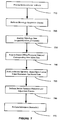
- FIG. 7 illustrates a flowchart depiction of a method in accordance with one illustrative embodiment of the present invention
- FIG. 8 illustrates a more detailed flowchart depiction of a method of performing a device operation prediction and adjustment process, as indicated in FIG. 7, in accordance with one illustrative embodiment of the present invention.
- FIG. 9 illustrates a more detailed flowchart depiction of a method of performing adjustment(s) based upon an error in an inline parameter, as indicated in FIG. 8, in accordance with one illustrative embodiment of the present invention.
- Embodiments of the present invention provide for adjusting and controlling inline process parameters relating to processing of semiconductor wafers 105 based upon device operation features of devices produced from the processed semiconductor wafers 105 .
- the operation parameters of a device such erase time, data access time, and the like, may be affected by a plurality of inline parameters, which may be correlated to particular device operation parameters and controlled.
- Embodiments of the present invention may be used to control several inline parameters, such as shallow isolation trench (STI) critical dimension (CD) parameter(s), tunnel oxidation parameter(s), source/drain critical dimension(s), film stack measurement(s), post etch critical dimension measurement(s), wafer electrical test parameter(s), and the like, which may be adjusted and controlled based upon device operation parameters.
- Embodiments of the present invention provide for performing substantially real time adjustments in an inline fashion during a process flow, based upon device operation parameters of devices produced from the processed semiconductor wafers 105 .
- a process controller 310 in the system 300 is capable of controlling various operations relating to a processing tool 610 .
- the system 300 is capable of acquiring manufacturing related data, such as metrology data, related to processed semiconductor wafers 105 , tool state data, and the like.
- the system 300 may also comprise a metrology tool 650 to acquire metrology data related to the processed semiconductor wafers 105 .
- the system 300 may also comprise a database unit 340 .
- the database unit 340 is provided for storing a plurality of types of data, such as manufacturing-related data, data related to the operation of the system 300 (e.g., the status of the processing tool 610 , the status of semiconductor wafers 105 , etc.).
- the database unit 340 may store tool state data relating to a plurality of process runs performed by the processing tool 610 .
- the database unit 340 may comprise a database server 342 for storing tool state data and/or other manufacturing data related to processing semiconductor wafers 105 , into a database storage unit 345 .
- the device-operation parameter/process-operation parameter correlation unit 320 may correlate a plurality of inline parameters relating to processing of semiconductor wafers 105 , such as the shallow-trench isolation (STI) critical dimension(s), the tunnel oxidization parameters, the first polygate critical dimension parameters, a source/drain critical dimension parameters, the oxide/nitride/oxide (ONO) film stack parameters, the post etch critical dimension parameters, and the like, to device operation parameters such as the erase time (EXE parameter) in memory devices such as flash memory devices.
- STI shallow-trench isolation
- the tunnel oxidization parameters such as the tunnel oxidization parameters
- the first polygate critical dimension parameters such as a source/drain critical dimension parameters
- the oxide/nitride/oxide (ONO) film stack parameters such as the post etch critical dimension parameters, and the like
- EXE parameter erase time
- the EXE parameters may provide an indication on how fast a write and an erase function performed upon a cell within a flash memory device may be executed, which may indirectly provide an indication of the power consumption of the flash memory device.
- the EXE parameter is an example of a device operation parameter that may be affected by the inline parameters described above.
- a process operation-to-device operation model 330 may perform a modeling of a characterization of the possible device operation parameter(s) based upon the inline parameters described above.
- the process operation-to-device operation model 330 is described in a more detailed block diagram in FIG. 4 and accompanying description below.
- the process operation-to-device operation model 330 may provide an indication of adjustments that may be made to one or more inline parameters based upon the device operation parameter data received by the system 300 .
- Adjustment data from the process operation-to-device operation model 330 may be provided to a feedback unit 360 and/or to a feed forward unit 350 .
- the feedback unit 360 is capable of receiving adjustment data and performing feedback adjustments to one or more processes performed by the manufacturing system 300 .
- the adjustments may include modifying one or more control input parameters used to control process operations performed by the system.
- the feed-forward unit 350 is capable of performing compensation adjustments to processing steps based upon adjustment data received from the process operation-to-device operation model 330 . Therefore, several inline parameters may be brought within a predetermined tolerance level to acquire a certain type of device operation parameter, such as an EXE parameter. Compensation adjustments made to subsequent processes performed on a previously processed semiconductor wafer 105 may be performed in a feed-forward manner.
- the process controller 310 , the device-operation parameter/process-operation parameter correlation unit 320 , process operation-to-device operation model 330 , the feedback unit 360 , and/or feed forward unit 350 may be software, hardware, or firmware units that are standalone units or may be integrated into a computer system associated with the system 300 .
- the various components represented by the blocks illustrated in FIG. 3 may communicate with one another via a system communications line 315 .
- the system communications line 315 may be a computer bus link, a dedicated hardware communications link, a telephone system communications link, a wireless communications link, or other communication links that may be implemented by those skilled in the art having benefit of the present disclosure.
- the process operation-to-device operation model 330 may comprise a device operation data interface 410 and a metrology data interface 420 .
- the device operation data interface 410 is capable of receiving data relating to operation parameters of devices manufactured from processed semiconductor wafers 105 (device operation parameter data) from a plurality of sources such as the database unit 340 and/or external data sources.
- the metrology data interface 420 may receive metrology data from a plurality of sources, such as the database unit 340 and/or the metrology tool 650 , in an inline fashion.
- An inline/offline parameter model 430 may model the behavior of one or more specific inline parameters to specific offline device operation parameters based upon the metrology data and the device operation data (modeling data).
- the inline/offline parameter model 430 is described in more detail in FIG. 5 and accompanying description below.
- the modeling data from the inline/offline parameter model 430 may then be received by a device operation parameter prediction unit 440 .
- the device operation parameter prediction unit 440 may predict the value(s) of one or more device operation parameters, such as the EXE parameter, or other data-access parameters relating to a memory device.
- the device operation parameter prediction unit 440 is capable of predicting the possible device operation parameters based upon the current inline state of the semiconductor wafers 105 being processed by the system 300 .
- a feedback adjustment calculation unit 450 may calculate feedback adjustment values that may be used to perform feedback adjustments upon processes to affect one or more inline parameters.
- the feed-forward adjustment calculation unit 460 may calculate several adjustment factors (feed-forward adjustment data) that may be used to modify the characteristics of several processed semiconductor wafers 105 using feed-forward adjustments.
- the feed-forward adjustments are generally performed through adjustments that are made to subsequent processes performed on the semiconductor wafers 105 , in order to affect the device operation parameters.
- the inline/offline parameter model 430 may comprise a plurality of sub-models that are capable of modeling the behavior of particular inline parameters in relation to particular offline parameters.
- the inline/offline parameter model 430 may comprise an STI CD-to-offline parameter model 510 , a tunnel oxidation layer-to-offline parameter model 520 , a first poly gate CD-to-offline parameter model 530 , a source/drain CD-to-offline parameter model 550 , an ONO film stack layer-to-offline parameter model 540 , a post etch CD-to-offline parameter model 560 , a wafer electrical test (WET)-to-offline parameter model 570 , and/or a multivariate model.
- WET wafer electrical test
- the models 510 - 570 may provide a modeling of the behavior of particular inline parameters and/or which may result in certain offline parameters, such as the EXE parameter in a flash memory device.
- the models 510 - 570 may also model the behavior of one or more inline parameters based upon predicted or actual device performance parameters.
- the models 510 - 570 may receive inline parameter information from the metrology tool 650 and/or the database unit 340 .
- the models 510 - 570 in one embodiment, may be used to affect the semiconductor wafers 105 such that devices manufactured from the processed semiconductor wafers 105 have more desirable operation parameters, such as improved EXE parameter(s).
- the model 510 may correlate one or more critical dimension measurements to one or more offline device operation parameters.
- the model 520 may correlate measurements relating to a tunnel oxidation layer to one or more offline device operation parameters.
- the model 530 may correlate polygate CD measurements to one or more offline device operation parameters.
- the model 540 may relate the thickness value of a ONO film stack layer to one or more offline device operation parameters.
- the ONO film stack layer generally refers to a dielectric layer that may comprise an Si 3 N 4 layer that is positioned between two SiO 2 layers.
- the model 560 may correlate a CD value relating to a source/drain structure formed on a semiconductor wafer 105 to one or more offline device operation parameters.
- the model 570 may correlate various electrical measurement (e.g., drive current measurements, etc.) to one or more offline device operation parameters.
- the model 580 may correlate various inline parameters described above to one or more offline device operation parameters.
- FIG. 6 a more detailed block diagram of the system 300 in accordance with one embodiment of the present invention is illustrated.
- Semiconductor wafers 105 are processed on processing tools 610 a , 610 b using a plurality of control input signals, or manufacturing parameters, provided via a line or network 623 .
- the control input signals, or manufacturing parameters, on the line 623 are sent to the processing tools 610 a , 610 b from a computer system 630 via machine interfaces 615 a , 615 b .
- the first and second machine interfaces 615 a , 615 b are generally located outside the processing tools 610 a , 610 b .
- the first and second machine interfaces 615 a , 615 b are located within the processing tools 610 a , 610 b .
- the semiconductor wafers 105 are provided to and carried from a plurality of processing tools 610 .
- semiconductor wafers 105 may be provided to a processing tool 610 manually.
- semiconductor wafers 105 may be provided to a processing tool 610 in an automatic fashion (e.g., robotic movement of semiconductor wafers 105 ).
- a plurality of semiconductor wafers 105 is transported in lots (e.g., stacked in cassettes) to the processing tools 610 .
- the computer system 630 sends control input signals, or manufacturing parameters, on the line 623 to the first and second machine interfaces 615 a , 615 b .
- the computer system 630 is capable of controlling processing operations.
- the computer system 630 is a process controller.
- the computer system 630 is coupled to a computer storage unit 632 that may contain a plurality of software programs and data sets.
- the computer system 630 may contain one or more processors (not shown) that are capable of performing the operations described herein.
- the computer system 630 employs a manufacturing model 640 to generate control input signals on the line 623 .
- the manufacturing model 640 contains a manufacturing recipe that determines a plurality of control input parameters that are sent on the line 623 to the processing tools 610 a , 610 b.
- the manufacturing model 640 defines a process script and input control that implement a particular manufacturing process.
- the control input signals (or control input parameters) on the line 623 that are intended for processing tool A 610 a are received and processed by the first machine interface 615 a .
- the control input signals on the line 623 that are intended for processing tool B 610 b are received and processed by the second machine interface 615 b .
- Examples of the processing tools 610 a , 610 b used in semiconductor manufacturing processes are steppers, etch process tools, deposition tools, and the like.
- One or more of the semiconductor wafers 105 that are processed by the processing tools 610 a , 610 b can also be sent to a metrology tool 650 for acquisition of metrology data.
- the metrology tool 650 may be a scatterometry data acquisition tool, an overlay-error measurement tool, a critical dimension measurement tool, and the like.
- a metrology tool 650 examines one or more processed semiconductor wafers 105 .
- the metrology data analysis unit 660 may collect, organize, and analyze data from the metrology tool 650 .
- the metrology data is directed to a variety of physical or electrical characteristics of the devices formed across the semiconductor wafers 105 .
- metrology data may be obtained as to line width measurements, depth of trenches, sidewall angles, thickness, resistance, and the like. Metrology data may be used to determine faults that may be present across the processed semiconductor wafers 105 , which may be used to quantify the performance of the processing tools 610 .
- the device-operation parameter/process-operation parameter correlation unit 320 receives data from the database unit 340 and the metrology data analysis unit 660 .
- the device-operation parameter/process-operation parameter correlation unit 320 correlates the inline metrology data and the device operation data and provides resultant data to the process operation-to-device operation model 330 .
- the process operation-to-device operation model 330 may then perform modeling of a plurality of inline parameters in relation to device operation parameter(s) (e.g., EXE parameter, etc.) using parameter prediction data and/or by actual performance data.
- the process operation-to-device operation model 330 may then provide feedback data to the feedback unit 360 and/or feed-forward data to the feed-forward unit 350 .
- the feed-forward unit 350 and the feedback unit 360 may then send data to the computer system 630 to implement feedback corrections to subsequent semiconductor wafers 105 , and/or to implement feed-forward adjustment compensation to processed semiconductor wafers 105 .
- the feedback and/or feed-forward adjustments may result in certain inline parameters being brought within acceptable tolerances such that device operation parameters have values that are within desired tolerance levels.
- the system 300 may process one or more semiconductor wafers 105 that may be associated with a batch/lot of semiconductor wafers 105 (block 710 ). Upon processing the semiconductor wafers 105 , the system 300 may acquire metrology data from one or more processed semiconductor wafers 105 (block 720 ). The system 300 may acquire metrology data from a sample of processed semiconductor wafers 105 and extrapolate inline metrology data to determine one or more inline parameters that may be representative of a group of processed semiconductor wafers 105 . The system 300 may then analyze the acquired metrology data to quantify inline parameters related to the processed semiconductor wafer 105 (block 730 ).
- the system 300 may store offline parameter data and acquire such data for analysis at a later time.
- the system 300 may acquire stored offline parameter data and corresponding prior inline data that may be correlated with stored offline parameter data (block 740 ).
- the system 300 may acquire current inline parameters on a real time or a near real time basis and correlate such data to certain offline parameters, such as device operation parameters.
- the system 300 may then perform an analysis of the device operation based upon current inline parameters and/or stored data that may provide additional inline parameters (block 750 ).
- the system 300 may perform a device operation predicting and adjustment process (block 760 ).
- a device operation prediction and adjustment process indicated in block 760 of FIG. 7 is provided in FIG. 8 and accompanying description below.
- the results of the device operation prediction and adjustment process include predicting possible device operation parameters and adjusting certain inline parameters, which may result in a determination of whether to perform adjustments to current processes based upon predicted device operation parameters, or continue current processing operations.
- the system 300 may perform subsequent processing of semiconductor wafers 105 throughout the manufacturing facility associated with the system 300 (block 770 ). The process described in FIG.
- the system 300 may analyze previous device operations based upon the stored data (block 810 ). Previous device operations may be correlated to previous inline parameters, therefore, a relationship between certain inline parameters and device operation parameters may be formulated for further prediction of possible device operation parameters. Based upon the analysis described above, the system 300 may predict device operation parameters of devices to be manufactured from currently processed semiconductor wafers 105 (block 820 ). This prediction of device operation parameters may be based upon current metrology analysis and may further be performed using the modeling processes described above.
- the process operation-to-device operation model 330 may provide a relationship analysis between several inline parameters to device operation of devices manufactured from processed semiconductor wafers 105 , such as memory devices, including flash memory devices.
- the system 300 may determine if one or more inline parameters is out of a desired range (block 830 ). In other words, the system 300 may analyze whether one or more inline parameters may cause the device operation parameter, such as the EXE parameter, to fall outside a desired range. The system 300 may analyze inline parameters and correlate them to predicted device operations. When the system 300 determines that one or more inline parameters may not be out of a desired range, the system 300 continues the current processing operations relating to the process flow in the system 300 (block 840 ). When the system 300 determines that one or more inline parameters may be outside of a desired range, the system 300 may perform adjustments to the process flow based upon the error discovered in one or more inline parameters (block 850 ). A more detailed description of the adjustments described in block 850 is provided in FIG. 9 and accompanying description below. The completion of the steps illustrated in FIG. 8, substantially completes the step of performing the device operation prediction and adjustment process indicated in block 760 of FIG. 7 .
- the system 300 determines adjustments to be made to specific processes within the process flow of the system 300 that may be made to correct the calculated error in the inline parameter (block 910 ). For example, the system 300 may provide or determine adjustments that may be made to a single process within the process flow to correct or bring the inline parameter within the desired acceptable range.
- the system 300 makes a determination whether any semiconductor wafers 105 in a batch or a lot remains to be processed (block 920 ).
- the system 300 determines that there are subsequent semiconductor wafers 105 in a batch/lot to be processed, the system 300 performs a feedback adjustment to correct the error on subsequent semiconductor wafers 105 in the batch (block 930 ). In this way, the subsequent semiconductor wafers 105 to be processed may be processed such that the inline error is not duplicated on those semiconductor wafers 105 .
- the system 300 may determine whether the error may be corrected using a subsequent process that may be performed on the processed semiconductor wafers 105 (block 940 ).
- an alarm may be initiated to alert the system operator (block 950 ).
- the operator may decide to scrap the semiconductor wafers 105 or rework the semiconductor wafers 105 based upon many factors, such as business rules, which may include factors such as the value of the semiconductor wafers 105 , the acceptable degradation in the devices manufactured from the semiconductor wafers 105 , the cost of the devices, etc.
- the system 300 may perform feed-forward compensation on the semiconductor wafers 105 to correct such errors (block 960 ). Based upon the feedback and/or feed-forward adjustment data, the inline parameters may be corrected such that predicted device operation parameters may be brought within an acceptable range of tolerance. The completion of the steps described in FIG. 9 substantially completes the step of performing adjustments based upon the error in the inline parameters as indicated in block 850 of FIG. 8 .
- a more efficient set of devices produced from processed semiconductor wafers 105 may be realized. Adjusting inline parameters to bring particular device operation parameters, such as the EXE parameters of a flash memory device, may be performed to increase the yield of devices that operate within acceptable and predetermined tolerances. Therefore, profitable devices, whose operations may depend or indicate how profitable a particular device may be, may be processed in a more efficient manner utilizing embodiments of the present invention.
- the principles taught by the present invention can be implemented in an Advanced Process Control (APC) Framework, such as a CATALYSTTM system offered by KLA TENCOR, INC.
- the CATALYSTTM system uses Semiconductor Equipment and Materials International (SEMI) Computer Integrated Manufacturing (CIM) Framework compliant system technologies, and is based on the Advanced Process Control (APC) Framework.
- the APC framework is a preferred platform from which to implement the control strategy taught by the present invention.
- the APC framework can be a factory-wide software system; therefore, the control strategies taught by the present invention can be applied to virtually any of the semiconductor manufacturing tools on the factory floor.
- the APC framework also allows for remote access and monitoring of the process performance.
- data storage can be more convenient, more flexible, and less expensive than local drives.
- the APC framework allows for more sophisticated types of control because it provides a significant amount of flexibility in writing the necessary software code.
- Deployment of the control strategy taught by the present invention onto the APC framework could require a number of software components.
- a computer script is written for each of the semiconductor manufacturing tools involved in the control system.
- a semiconductor manufacturing tool in the control system When a semiconductor manufacturing tool in the control system is started in the semiconductor manufacturing fab, it generally calls upon a script to initiate the action that is required by the process controller, such as the overlay controller.
- the control methods are generally defined and performed in these scripts.
- the development of these scripts can comprise a significant portion of the development of a control system.
- the principles taught by the present invention can be implemented into other types of manufacturing frameworks.
Abstract
Description
Claims (30)
Priority Applications (4)
| Application Number | Priority Date | Filing Date | Title |
|---|---|---|---|
| US10/254,209 US6810296B2 (en) | 2002-09-25 | 2002-09-25 | Correlating an inline parameter to a device operation parameter |
| AU2003270664A AU2003270664A1 (en) | 2002-09-25 | 2003-09-18 | Correlating an inline parameter to a device operation parameter in semiconductor processing |
| PCT/US2003/028935 WO2004030081A1 (en) | 2002-09-25 | 2003-09-18 | Correlating an inline parameter to a device operation parameter in semiconductor processing |
| TW092126290A TW200413977A (en) | 2002-09-25 | 2003-09-24 | Correlating an inline parameter to a device operation parameter |
Applications Claiming Priority (1)
| Application Number | Priority Date | Filing Date | Title |
|---|---|---|---|
| US10/254,209 US6810296B2 (en) | 2002-09-25 | 2002-09-25 | Correlating an inline parameter to a device operation parameter |
Publications (2)
| Publication Number | Publication Date |
|---|---|
| US20040059456A1 US20040059456A1 (en) | 2004-03-25 |
| US6810296B2 true US6810296B2 (en) | 2004-10-26 |
Family
ID=31993294
Family Applications (1)
| Application Number | Title | Priority Date | Filing Date |
|---|---|---|---|
| US10/254,209 Expired - Lifetime US6810296B2 (en) | 2002-09-25 | 2002-09-25 | Correlating an inline parameter to a device operation parameter |
Country Status (4)
| Country | Link |
|---|---|
| US (1) | US6810296B2 (en) |
| AU (1) | AU2003270664A1 (en) |
| TW (1) | TW200413977A (en) |
| WO (1) | WO2004030081A1 (en) |
Cited By (21)
| Publication number | Priority date | Publication date | Assignee | Title |
|---|---|---|---|---|
| US20050010319A1 (en) * | 2003-07-09 | 2005-01-13 | Sukesh Patel | System and method for validating and visualizing APC assisted semiconductor manufacturing processes |
| US20050071036A1 (en) * | 2003-09-30 | 2005-03-31 | Tokyo Electron Limited | System and method for using first-principles simulation to characterize a semiconductor manufacturing process |
| US20050071035A1 (en) * | 2003-09-30 | 2005-03-31 | Tokyo Electron Limited | System and method for using first-principles simulation to control a semiconductor manufacturing process |
| US20050071038A1 (en) * | 2003-09-30 | 2005-03-31 | Tokyo Electron Limited | System and method for using first-principles simulation to control a semiconductor manufacturing process |
| US7109046B1 (en) * | 2004-01-30 | 2006-09-19 | Advanced Micro Devices, Inc. | Surface oxide tabulation and photo process control and cost savings |
| US20070265725A1 (en) * | 2006-05-15 | 2007-11-15 | Taiwan Semiconductor Manufacturing Company, Ltd. | Model Import for Electronic Design Automation |
| US20080061251A1 (en) * | 2006-06-09 | 2008-03-13 | Christopher Burgess | Ion beams in an ion implanter |
| US20080275585A1 (en) * | 2007-05-04 | 2008-11-06 | Taiwan Semiconductor Manufacturing Company, Ltd. | Extraction of key process parameter |
| US20080319568A1 (en) * | 2007-06-22 | 2008-12-25 | International Business Machines Corporation | Method and system for creating array defect paretos using electrical overlay of bitfail maps, photo limited yield, yield, and auto pattern recognition code data |
| US20090005888A1 (en) * | 2007-06-29 | 2009-01-01 | Patel Nital S | Configurable advanced process control |
| US20090222785A1 (en) * | 2008-02-28 | 2009-09-03 | Taiwan Semiconductor Manufacturing Company, Ltd. | Method for shape and timing equivalent dimension extraction |
| US20090299670A1 (en) * | 2008-06-03 | 2009-12-03 | Sony Corporation | Process control device and process control method |
| US20100095253A1 (en) * | 2008-10-13 | 2010-04-15 | Taiwan Semiconductor Manufacturing Company, Ltd. | Table-based dfm for accurate post-layout analysis |
| US20110124193A1 (en) * | 2009-11-25 | 2011-05-26 | Taiwan Semiconductor Manufacturing Company, Ltd. | Customized patterning modulation and optimization |
| US20110161907A1 (en) * | 2009-12-28 | 2011-06-30 | Taiwan Semiconductor Manufacturing Company, Ltd. | Practical Approach to Layout Migration |
| US8032348B2 (en) * | 2003-09-30 | 2011-10-04 | Tokyo Electron Limited | System and method for using first-principles simulation to facilitate a semiconductor manufacturing process |
| US20110243424A1 (en) * | 2010-04-01 | 2011-10-06 | Taiwan Semiconductor Manufacturing Company, Ltd. ("Tsmc") | Method and apparatus for monitoring mask process impact on lithography performance |
| US8145337B2 (en) | 2007-05-04 | 2012-03-27 | Taiwan Semiconductor Manufacturing Company, Ltd. | Methodology to enable wafer result prediction of semiconductor wafer batch processing equipment |
| CN101581930B (en) * | 2008-02-05 | 2012-07-18 | 台湾积体电路制造股份有限公司 | Novel methodology to realize automatic virtual metrology |
| US20130297061A1 (en) * | 2012-05-03 | 2013-11-07 | National Taiwan University | Method and computer-aided design system of manufacturing an optical system |
| US8615314B1 (en) * | 2004-09-02 | 2013-12-24 | Advanced Micro Devices, Inc. | Process control using analysis of an upstream process |
Families Citing this family (14)
| Publication number | Priority date | Publication date | Assignee | Title |
|---|---|---|---|---|
| US20040088068A1 (en) * | 2002-10-31 | 2004-05-06 | Daniel Kadosh | Method and apparatus for providing first-principles feed-forward manufacturing control |
| US20050021272A1 (en) * | 2003-07-07 | 2005-01-27 | Jenkins Naomi M. | Method and apparatus for performing metrology dispatching based upon fault detection |
| US7822500B2 (en) * | 2004-06-21 | 2010-10-26 | Ebara Corporation | Polishing apparatus and polishing method |
| US7296103B1 (en) * | 2004-10-05 | 2007-11-13 | Advanced Micro Devices, Inc. | Method and system for dynamically selecting wafer lots for metrology processing |
| US20070239305A1 (en) * | 2006-03-28 | 2007-10-11 | Haoren Zhuang | Process control systems and methods |
| US8156450B2 (en) * | 2006-12-18 | 2012-04-10 | Cadence Design Systems, Inc. | Method and system for mask optimization |
| US8146024B2 (en) * | 2006-12-18 | 2012-03-27 | Cadence Design Systems, Inc. | Method and system for process optimization |
| US7694244B2 (en) | 2006-12-18 | 2010-04-06 | Cadence Design Systems, Inc. | Modeling and cross correlation of design predicted criticalities for optimization of semiconductor manufacturing |
| US7665048B2 (en) * | 2006-12-18 | 2010-02-16 | Cadence Design Systems, Inc. | Method and system for inspection optimization in design and production of integrated circuits |
| US8669497B2 (en) * | 2007-03-30 | 2014-03-11 | Tokyo Electron Limited | Apparatus and method for predictive temperature correction during thermal processing |
| DE102008021556B4 (en) * | 2008-04-30 | 2019-06-06 | Advanced Micro Devices, Inc. | Method and system for two-stage prediction of a quality distribution of semiconductor devices |
| US9477219B2 (en) * | 2010-03-25 | 2016-10-25 | Taiwan Semiconductor Manufacturing Company, Ltd. | Dynamic compensation in advanced process control |
| US9689923B2 (en) * | 2013-08-03 | 2017-06-27 | Kla-Tencor Corp. | Adaptive electrical testing of wafers |
| US9824940B2 (en) * | 2015-09-30 | 2017-11-21 | Taiwan Semiconductor Manufacturing Co., Ltd. | Intelligent metrology based on module knowledge |
Citations (16)
| Publication number | Priority date | Publication date | Assignee | Title |
|---|---|---|---|---|
| US3614640A (en) * | 1970-01-27 | 1971-10-19 | Us Navy | Frequency discriminator using no inductive components |
| US4578648A (en) * | 1984-04-16 | 1986-03-25 | Werrbach Donn R | Dynamic verification gate circuit |
| US5396433A (en) * | 1993-04-07 | 1995-03-07 | Nec Corporation | Apparatus and method for assembling and checking microwave monolithic integrated circuit (MMIC) module |
| US5482881A (en) * | 1995-03-14 | 1996-01-09 | Advanced Micro Devices, Inc. | Method of making flash EEPROM memory with reduced column leakage current |
| US5810928A (en) * | 1994-11-21 | 1998-09-22 | Mitsubishi Corporation | Method of measuring gas component concentrations of special material gases for semiconductor, a semiconductor equipment, and an apparatus for supplying special material gases for semiconductor |
| US5838445A (en) * | 1995-06-07 | 1998-11-17 | Micron Technology, Inc. | Method and apparatus for determining surface roughness |
| US6020264A (en) * | 1997-01-31 | 2000-02-01 | International Business Machines Corporation | Method and apparatus for in-line oxide thickness determination in chemical-mechanical polishing |
| US20020051567A1 (en) * | 2000-09-04 | 2002-05-02 | Dietmar Ganz | Method of adjusting a lithographic tool |
| US6409576B1 (en) * | 1999-07-26 | 2002-06-25 | Ebara Corporation | Polishing apparatus |
| US20020082738A1 (en) * | 2000-12-27 | 2002-06-27 | Insyst Ltd. | Method for global automated process control |
| US20020088952A1 (en) * | 2000-11-15 | 2002-07-11 | Rao Nagaraja P. | Optical method and apparatus for inspecting large area planar objects |
| US6486492B1 (en) * | 1999-06-29 | 2002-11-26 | Applied Materials, Inc. | Integrated critical dimension control for semiconductor device manufacturing |
| US20020192966A1 (en) * | 2001-06-19 | 2002-12-19 | Shanmugasundram Arulkumar P. | In situ sensor based control of semiconductor processing procedure |
| US20030097198A1 (en) * | 2001-11-16 | 2003-05-22 | Sonderman Thomas J. | Method and apparatus for utilizing integrated metrology data as feed-forward data |
| US6594598B1 (en) * | 1997-10-08 | 2003-07-15 | Matsushita Electronics Corporation | Method for controlling production line |
| US6638778B1 (en) * | 2002-02-25 | 2003-10-28 | Advanced Micro Devices, Inc. | Method for determining, tracking and/or controlling processing based upon silicon characteristics |
Family Cites Families (4)
| Publication number | Priority date | Publication date | Assignee | Title |
|---|---|---|---|---|
| US5646870A (en) * | 1995-02-13 | 1997-07-08 | Advanced Micro Devices, Inc. | Method for setting and adjusting process parameters to maintain acceptable critical dimensions across each die of mass-produced semiconductor wafers |
| US5926690A (en) * | 1997-05-28 | 1999-07-20 | Advanced Micro Devices, Inc. | Run-to-run control process for controlling critical dimensions |
| US6041270A (en) * | 1997-12-05 | 2000-03-21 | Advanced Micro Devices, Inc. | Automatic recipe adjust and download based on process control window |
| US6245581B1 (en) * | 2000-04-19 | 2001-06-12 | Advanced Micro Devices, Inc. | Method and apparatus for control of critical dimension using feedback etch control |
-
2002
- 2002-09-25 US US10/254,209 patent/US6810296B2/en not_active Expired - Lifetime
-
2003
- 2003-09-18 WO PCT/US2003/028935 patent/WO2004030081A1/en not_active Application Discontinuation
- 2003-09-18 AU AU2003270664A patent/AU2003270664A1/en not_active Abandoned
- 2003-09-24 TW TW092126290A patent/TW200413977A/en unknown
Patent Citations (16)
| Publication number | Priority date | Publication date | Assignee | Title |
|---|---|---|---|---|
| US3614640A (en) * | 1970-01-27 | 1971-10-19 | Us Navy | Frequency discriminator using no inductive components |
| US4578648A (en) * | 1984-04-16 | 1986-03-25 | Werrbach Donn R | Dynamic verification gate circuit |
| US5396433A (en) * | 1993-04-07 | 1995-03-07 | Nec Corporation | Apparatus and method for assembling and checking microwave monolithic integrated circuit (MMIC) module |
| US5810928A (en) * | 1994-11-21 | 1998-09-22 | Mitsubishi Corporation | Method of measuring gas component concentrations of special material gases for semiconductor, a semiconductor equipment, and an apparatus for supplying special material gases for semiconductor |
| US5482881A (en) * | 1995-03-14 | 1996-01-09 | Advanced Micro Devices, Inc. | Method of making flash EEPROM memory with reduced column leakage current |
| US5838445A (en) * | 1995-06-07 | 1998-11-17 | Micron Technology, Inc. | Method and apparatus for determining surface roughness |
| US6020264A (en) * | 1997-01-31 | 2000-02-01 | International Business Machines Corporation | Method and apparatus for in-line oxide thickness determination in chemical-mechanical polishing |
| US6594598B1 (en) * | 1997-10-08 | 2003-07-15 | Matsushita Electronics Corporation | Method for controlling production line |
| US6486492B1 (en) * | 1999-06-29 | 2002-11-26 | Applied Materials, Inc. | Integrated critical dimension control for semiconductor device manufacturing |
| US6409576B1 (en) * | 1999-07-26 | 2002-06-25 | Ebara Corporation | Polishing apparatus |
| US20020051567A1 (en) * | 2000-09-04 | 2002-05-02 | Dietmar Ganz | Method of adjusting a lithographic tool |
| US20020088952A1 (en) * | 2000-11-15 | 2002-07-11 | Rao Nagaraja P. | Optical method and apparatus for inspecting large area planar objects |
| US20020082738A1 (en) * | 2000-12-27 | 2002-06-27 | Insyst Ltd. | Method for global automated process control |
| US20020192966A1 (en) * | 2001-06-19 | 2002-12-19 | Shanmugasundram Arulkumar P. | In situ sensor based control of semiconductor processing procedure |
| US20030097198A1 (en) * | 2001-11-16 | 2003-05-22 | Sonderman Thomas J. | Method and apparatus for utilizing integrated metrology data as feed-forward data |
| US6638778B1 (en) * | 2002-02-25 | 2003-10-28 | Advanced Micro Devices, Inc. | Method for determining, tracking and/or controlling processing based upon silicon characteristics |
Non-Patent Citations (2)
| Title |
|---|
| Bloom, "2-Bit Cell NV Memory Minimizes Chip Area with Less Masks" Jan. 2002, Nikkei Business Publications, Inc. * |
| Wan, "Comparison of self-aligned and non-self-aligned E/D MESFETs" May 1989, Electron Devices, vol. 36, Issue 5, pp. 839-845.* * |
Cited By (41)
| Publication number | Priority date | Publication date | Assignee | Title |
|---|---|---|---|---|
| US20050010319A1 (en) * | 2003-07-09 | 2005-01-13 | Sukesh Patel | System and method for validating and visualizing APC assisted semiconductor manufacturing processes |
| US20050071036A1 (en) * | 2003-09-30 | 2005-03-31 | Tokyo Electron Limited | System and method for using first-principles simulation to characterize a semiconductor manufacturing process |
| US20050071035A1 (en) * | 2003-09-30 | 2005-03-31 | Tokyo Electron Limited | System and method for using first-principles simulation to control a semiconductor manufacturing process |
| US20050071039A1 (en) * | 2003-09-30 | 2005-03-31 | Tokyo Electron Limited | System and method for using first-principles simulation to provide virtual sensors that facilitate a semiconductor manufacturing process |
| US20050071038A1 (en) * | 2003-09-30 | 2005-03-31 | Tokyo Electron Limited | System and method for using first-principles simulation to control a semiconductor manufacturing process |
| US8036869B2 (en) * | 2003-09-30 | 2011-10-11 | Tokyo Electron Limited | System and method for using first-principles simulation to control a semiconductor manufacturing process via a simulation result or a derived empirical model |
| US8050900B2 (en) * | 2003-09-30 | 2011-11-01 | Tokyo Electron Limited | System and method for using first-principles simulation to provide virtual sensors that facilitate a semiconductor manufacturing process |
| US8032348B2 (en) * | 2003-09-30 | 2011-10-04 | Tokyo Electron Limited | System and method for using first-principles simulation to facilitate a semiconductor manufacturing process |
| US8014991B2 (en) * | 2003-09-30 | 2011-09-06 | Tokyo Electron Limited | System and method for using first-principles simulation to characterize a semiconductor manufacturing process |
| US8073667B2 (en) * | 2003-09-30 | 2011-12-06 | Tokyo Electron Limited | System and method for using first-principles simulation to control a semiconductor manufacturing process |
| US7109046B1 (en) * | 2004-01-30 | 2006-09-19 | Advanced Micro Devices, Inc. | Surface oxide tabulation and photo process control and cost savings |
| US8615314B1 (en) * | 2004-09-02 | 2013-12-24 | Advanced Micro Devices, Inc. | Process control using analysis of an upstream process |
| US20070265725A1 (en) * | 2006-05-15 | 2007-11-15 | Taiwan Semiconductor Manufacturing Company, Ltd. | Model Import for Electronic Design Automation |
| US8352888B2 (en) | 2006-05-15 | 2013-01-08 | Taiwan Semiconductor Manufacturing Company, Ltd. | Model import for electronic design automation |
| US8214772B2 (en) | 2006-05-15 | 2012-07-03 | Taiwan Semiconductor Manufacturing Company, Ltd. | Model import for electronic design automation |
| US7954072B2 (en) | 2006-05-15 | 2011-05-31 | Taiwan Semiconductor Manufacturing Company, Ltd. | Model import for electronic design automation |
| US20110230998A1 (en) * | 2006-05-15 | 2011-09-22 | Taiwan Semiconductor Manufacturing Company, Ltd. | Model import for electronic design automation |
| US20110231804A1 (en) * | 2006-05-15 | 2011-09-22 | Taiwan Semiconductor Manufacturing Company, Ltd. | Model import for electronic design automation |
| US7709817B2 (en) * | 2006-06-09 | 2010-05-04 | Applied Materials, Inc. | Ion beams in an ion implanter |
| US20080061251A1 (en) * | 2006-06-09 | 2008-03-13 | Christopher Burgess | Ion beams in an ion implanter |
| US8145337B2 (en) | 2007-05-04 | 2012-03-27 | Taiwan Semiconductor Manufacturing Company, Ltd. | Methodology to enable wafer result prediction of semiconductor wafer batch processing equipment |
| US7974728B2 (en) | 2007-05-04 | 2011-07-05 | Taiwan Semiconductor Manufacturing Company, Ltd. | System for extraction of key process parameters from fault detection classification to enable wafer prediction |
| US8682466B2 (en) * | 2007-05-04 | 2014-03-25 | Taiwan Semiconductor Manufacturing Company, Ltd. | Automatic virtual metrology for semiconductor wafer result prediction |
| US20080275585A1 (en) * | 2007-05-04 | 2008-11-06 | Taiwan Semiconductor Manufacturing Company, Ltd. | Extraction of key process parameter |
| US20080319568A1 (en) * | 2007-06-22 | 2008-12-25 | International Business Machines Corporation | Method and system for creating array defect paretos using electrical overlay of bitfail maps, photo limited yield, yield, and auto pattern recognition code data |
| US20090005888A1 (en) * | 2007-06-29 | 2009-01-01 | Patel Nital S | Configurable advanced process control |
| CN101581930B (en) * | 2008-02-05 | 2012-07-18 | 台湾积体电路制造股份有限公司 | Novel methodology to realize automatic virtual metrology |
| US8037575B2 (en) | 2008-02-28 | 2011-10-18 | Taiwan Semiconductor Manufacturing Company, Ltd. | Method for shape and timing equivalent dimension extraction |
| US20090222785A1 (en) * | 2008-02-28 | 2009-09-03 | Taiwan Semiconductor Manufacturing Company, Ltd. | Method for shape and timing equivalent dimension extraction |
| US20090299670A1 (en) * | 2008-06-03 | 2009-12-03 | Sony Corporation | Process control device and process control method |
| US8001494B2 (en) | 2008-10-13 | 2011-08-16 | Taiwan Semiconductor Manufacturing Company, Ltd. | Table-based DFM for accurate post-layout analysis |
| US8201111B2 (en) | 2008-10-13 | 2012-06-12 | Taiwan Semiconductor Manufacturing Company, Ltd. | Table-based DFM for accurate post-layout analysis |
| US20100095253A1 (en) * | 2008-10-13 | 2010-04-15 | Taiwan Semiconductor Manufacturing Company, Ltd. | Table-based dfm for accurate post-layout analysis |
| US8806386B2 (en) | 2009-11-25 | 2014-08-12 | Taiwan Semiconductor Manufacturing Company, Ltd. | Customized patterning modulation and optimization |
| US20110124193A1 (en) * | 2009-11-25 | 2011-05-26 | Taiwan Semiconductor Manufacturing Company, Ltd. | Customized patterning modulation and optimization |
| US20110161907A1 (en) * | 2009-12-28 | 2011-06-30 | Taiwan Semiconductor Manufacturing Company, Ltd. | Practical Approach to Layout Migration |
| US8745554B2 (en) | 2009-12-28 | 2014-06-03 | Taiwan Semiconductor Manufacturing Company, Ltd. | Practical approach to layout migration |
| US8681326B2 (en) * | 2010-04-01 | 2014-03-25 | Taiwan Semiconductor Manufacturing Company, Ltd. | Method and apparatus for monitoring mask process impact on lithography performance |
| US8477299B2 (en) * | 2010-04-01 | 2013-07-02 | Taiwan Semiconductor Manufacturing Company, Ltd. | Method and apparatus for monitoring mask process impact on lithography performance |
| US20110243424A1 (en) * | 2010-04-01 | 2011-10-06 | Taiwan Semiconductor Manufacturing Company, Ltd. ("Tsmc") | Method and apparatus for monitoring mask process impact on lithography performance |
| US20130297061A1 (en) * | 2012-05-03 | 2013-11-07 | National Taiwan University | Method and computer-aided design system of manufacturing an optical system |
Also Published As
| Publication number | Publication date |
|---|---|
| AU2003270664A1 (en) | 2004-04-19 |
| TW200413977A (en) | 2004-08-01 |
| US20040059456A1 (en) | 2004-03-25 |
| WO2004030081A1 (en) | 2004-04-08 |
Similar Documents
| Publication | Publication Date | Title |
|---|---|---|
| US6810296B2 (en) | Correlating an inline parameter to a device operation parameter | |
| US6751518B1 (en) | Dynamic process state adjustment of a processing tool to reduce non-uniformity | |
| US6773931B2 (en) | Dynamic targeting for a process control system | |
| US6304999B1 (en) | Method and apparatus for embedded process control framework in tool systems | |
| US6708075B2 (en) | Method and apparatus for utilizing integrated metrology data as feed-forward data | |
| US8017411B2 (en) | Dynamic adaptive sampling rate for model prediction | |
| US6610550B1 (en) | Method and apparatus for correlating error model with defect data | |
| US6560503B1 (en) | Method and apparatus for monitoring controller performance using statistical process control | |
| US20060095232A1 (en) | Fault detection through feedback | |
| US6708129B1 (en) | Method and apparatus for wafer-to-wafer control with partial measurement data | |
| US6756243B2 (en) | Method and apparatus for cascade control using integrated metrology | |
| US6740534B1 (en) | Determination of a process flow based upon fault detection analysis | |
| US6597447B1 (en) | Method and apparatus for periodic correction of metrology data | |
| US6947803B1 (en) | Dispatch and/or disposition of material based upon an expected parameter result | |
| US6645780B1 (en) | Method and apparatus for combining integrated and offline metrology for process control | |
| US7254453B2 (en) | Secondary process controller for supplementing a primary process controller | |
| US6834213B1 (en) | Process control based upon a metrology delay | |
| US6905895B1 (en) | Predicting process excursions based upon tool state variables | |
| US6698009B1 (en) | Method and apparatus for modeling of batch dynamics based upon integrated metrology | |
| US6571371B1 (en) | Method and apparatus for using latency time as a run-to-run control parameter | |
| US6957120B1 (en) | Multi-level process data representation | |
| US6890773B1 (en) | Dynamic maintenance of manufacturing system components | |
| US6834211B1 (en) | Adjusting a trace data rate based upon a tool state | |
| US7720559B1 (en) | Dynamic tool scheduling based upon defects | |
| US6788988B1 (en) | Method and apparatus using integrated metrology data for pre-process and post-process control |
Legal Events
| Date | Code | Title | Description |
|---|---|---|---|
| STCF | Information on status: patent grant |
Free format text: PATENTED CASE |
|
| FPAY | Fee payment |
Year of fee payment: 4 |
|
| AS | Assignment |
Owner name: GLOBALFOUNDRIES INC., CAYMAN ISLANDS Free format text: AFFIRMATION OF PATENT ASSIGNMENT;ASSIGNOR:ADVANCED MICRO DEVICES, INC.;REEL/FRAME:023119/0083 Effective date: 20090630 |
|
| FPAY | Fee payment |
Year of fee payment: 8 |
|
| FPAY | Fee payment |
Year of fee payment: 12 |
|
| AS | Assignment |
Owner name: WILMINGTON TRUST, NATIONAL ASSOCIATION, DELAWARE Free format text: SECURITY AGREEMENT;ASSIGNOR:GLOBALFOUNDRIES INC.;REEL/FRAME:049490/0001 Effective date: 20181127 |
|
| AS | Assignment |
Owner name: GLOBALFOUNDRIES U.S. INC., CALIFORNIA Free format text: ASSIGNMENT OF ASSIGNORS INTEREST;ASSIGNOR:GLOBALFOUNDRIES INC.;REEL/FRAME:054633/0001 Effective date: 20201022 |
|
| AS | Assignment |
Owner name: GLOBALFOUNDRIES INC., CAYMAN ISLANDS Free format text: RELEASE BY SECURED PARTY;ASSIGNOR:WILMINGTON TRUST, NATIONAL ASSOCIATION;REEL/FRAME:054636/0001 Effective date: 20201117 |
|
| AS | Assignment |
Owner name: GLOBALFOUNDRIES U.S. INC., NEW YORK Free format text: RELEASE BY SECURED PARTY;ASSIGNOR:WILMINGTON TRUST, NATIONAL ASSOCIATION;REEL/FRAME:056987/0001 Effective date: 20201117 |