US6807349B2 - Planer waveguide and method of formation - Google Patents
Planer waveguide and method of formation Download PDFInfo
- Publication number
- US6807349B2 US6807349B2 US09/946,712 US94671201A US6807349B2 US 6807349 B2 US6807349 B2 US 6807349B2 US 94671201 A US94671201 A US 94671201A US 6807349 B2 US6807349 B2 US 6807349B2
- Authority
- US
- United States
- Prior art keywords
- waveguide
- temperature
- region
- core
- pecvd
- Prior art date
- Legal status (The legal status is an assumption and is not a legal conclusion. Google has not performed a legal analysis and makes no representation as to the accuracy of the status listed.)
- Expired - Fee Related, expires
Links
- 238000000034 method Methods 0.000 title claims abstract description 62
- 230000015572 biosynthetic process Effects 0.000 title claims abstract description 18
- 238000010438 heat treatment Methods 0.000 claims abstract description 34
- 230000003287 optical effect Effects 0.000 claims abstract description 31
- 239000000463 material Substances 0.000 claims abstract description 26
- VYPSYNLAJGMNEJ-UHFFFAOYSA-N Silicium dioxide Chemical compound O=[Si]=O VYPSYNLAJGMNEJ-UHFFFAOYSA-N 0.000 claims abstract description 24
- 238000002844 melting Methods 0.000 claims abstract description 22
- 230000008018 melting Effects 0.000 claims abstract description 22
- 238000000137 annealing Methods 0.000 claims abstract description 16
- 239000000377 silicon dioxide Substances 0.000 claims abstract description 12
- 239000010409 thin film Substances 0.000 claims abstract description 9
- 238000005334 plasma enhanced chemical vapour deposition Methods 0.000 claims description 28
- 238000000623 plasma-assisted chemical vapour deposition Methods 0.000 claims description 28
- 230000008569 process Effects 0.000 claims description 25
- 238000005253 cladding Methods 0.000 claims description 9
- IJGRMHOSHXDMSA-UHFFFAOYSA-N Atomic nitrogen Chemical compound N#N IJGRMHOSHXDMSA-UHFFFAOYSA-N 0.000 claims description 6
- XUIMIQQOPSSXEZ-UHFFFAOYSA-N Silicon Chemical compound [Si] XUIMIQQOPSSXEZ-UHFFFAOYSA-N 0.000 claims description 5
- BOTDANWDWHJENH-UHFFFAOYSA-N Tetraethyl orthosilicate Chemical compound CCO[Si](OCC)(OCC)OCC BOTDANWDWHJENH-UHFFFAOYSA-N 0.000 claims description 5
- 239000007788 liquid Substances 0.000 claims description 5
- 229910052710 silicon Inorganic materials 0.000 claims description 5
- 239000010703 silicon Substances 0.000 claims description 5
- 229910052757 nitrogen Inorganic materials 0.000 claims description 3
- 239000011159 matrix material Substances 0.000 claims description 2
- QJGQUHMNIGDVPM-UHFFFAOYSA-N nitrogen group Chemical group [N] QJGQUHMNIGDVPM-UHFFFAOYSA-N 0.000 claims description 2
- 230000010287 polarization Effects 0.000 claims description 2
- 239000010410 layer Substances 0.000 description 11
- 238000000151 deposition Methods 0.000 description 7
- 238000009966 trimming Methods 0.000 description 7
- 230000002427 irreversible effect Effects 0.000 description 5
- 230000008021 deposition Effects 0.000 description 4
- 238000004519 manufacturing process Methods 0.000 description 4
- 239000002243 precursor Substances 0.000 description 3
- 239000000758 substrate Substances 0.000 description 3
- 230000008859 change Effects 0.000 description 2
- 238000001816 cooling Methods 0.000 description 2
- 239000002019 doping agent Substances 0.000 description 2
- 238000012986 modification Methods 0.000 description 2
- 230000004048 modification Effects 0.000 description 2
- 230000002441 reversible effect Effects 0.000 description 2
- 230000008901 benefit Effects 0.000 description 1
- 239000012792 core layer Substances 0.000 description 1
- 230000001419 dependent effect Effects 0.000 description 1
- 238000005137 deposition process Methods 0.000 description 1
- 238000012631 diagnostic technique Methods 0.000 description 1
- 230000000694 effects Effects 0.000 description 1
- 238000005530 etching Methods 0.000 description 1
- 230000004907 flux Effects 0.000 description 1
- 230000007062 hydrolysis Effects 0.000 description 1
- 238000006460 hydrolysis reaction Methods 0.000 description 1
- 238000010849 ion bombardment Methods 0.000 description 1
- 230000010363 phase shift Effects 0.000 description 1
- 239000000843 powder Substances 0.000 description 1
- 230000009897 systematic effect Effects 0.000 description 1
Images


Classifications
-
- G—PHYSICS
- G02—OPTICS
- G02B—OPTICAL ELEMENTS, SYSTEMS OR APPARATUS
- G02B6/00—Light guides; Structural details of arrangements comprising light guides and other optical elements, e.g. couplings
- G02B6/10—Light guides; Structural details of arrangements comprising light guides and other optical elements, e.g. couplings of the optical waveguide type
- G02B6/12—Light guides; Structural details of arrangements comprising light guides and other optical elements, e.g. couplings of the optical waveguide type of the integrated circuit kind
- G02B6/12007—Light guides; Structural details of arrangements comprising light guides and other optical elements, e.g. couplings of the optical waveguide type of the integrated circuit kind forming wavelength selective elements, e.g. multiplexer, demultiplexer
- G02B6/12009—Light guides; Structural details of arrangements comprising light guides and other optical elements, e.g. couplings of the optical waveguide type of the integrated circuit kind forming wavelength selective elements, e.g. multiplexer, demultiplexer comprising arrayed waveguide grating [AWG] devices, i.e. with a phased array of waveguides
- G02B6/12011—Light guides; Structural details of arrangements comprising light guides and other optical elements, e.g. couplings of the optical waveguide type of the integrated circuit kind forming wavelength selective elements, e.g. multiplexer, demultiplexer comprising arrayed waveguide grating [AWG] devices, i.e. with a phased array of waveguides characterised by the arrayed waveguides, e.g. comprising a filled groove in the array section
-
- G—PHYSICS
- G02—OPTICS
- G02B—OPTICAL ELEMENTS, SYSTEMS OR APPARATUS
- G02B6/00—Light guides; Structural details of arrangements comprising light guides and other optical elements, e.g. couplings
- G02B6/10—Light guides; Structural details of arrangements comprising light guides and other optical elements, e.g. couplings of the optical waveguide type
- G02B6/12—Light guides; Structural details of arrangements comprising light guides and other optical elements, e.g. couplings of the optical waveguide type of the integrated circuit kind
- G02B6/12007—Light guides; Structural details of arrangements comprising light guides and other optical elements, e.g. couplings of the optical waveguide type of the integrated circuit kind forming wavelength selective elements, e.g. multiplexer, demultiplexer
- G02B6/12009—Light guides; Structural details of arrangements comprising light guides and other optical elements, e.g. couplings of the optical waveguide type of the integrated circuit kind forming wavelength selective elements, e.g. multiplexer, demultiplexer comprising arrayed waveguide grating [AWG] devices, i.e. with a phased array of waveguides
- G02B6/12033—Light guides; Structural details of arrangements comprising light guides and other optical elements, e.g. couplings of the optical waveguide type of the integrated circuit kind forming wavelength selective elements, e.g. multiplexer, demultiplexer comprising arrayed waveguide grating [AWG] devices, i.e. with a phased array of waveguides characterised by means for configuring the device, e.g. moveable element for wavelength tuning
-
- G—PHYSICS
- G02—OPTICS
- G02B—OPTICAL ELEMENTS, SYSTEMS OR APPARATUS
- G02B6/00—Light guides; Structural details of arrangements comprising light guides and other optical elements, e.g. couplings
- G02B6/10—Light guides; Structural details of arrangements comprising light guides and other optical elements, e.g. couplings of the optical waveguide type
- G02B6/12—Light guides; Structural details of arrangements comprising light guides and other optical elements, e.g. couplings of the optical waveguide type of the integrated circuit kind
- G02B6/122—Basic optical elements, e.g. light-guiding paths
-
- G—PHYSICS
- G02—OPTICS
- G02B—OPTICAL ELEMENTS, SYSTEMS OR APPARATUS
- G02B6/00—Light guides; Structural details of arrangements comprising light guides and other optical elements, e.g. couplings
- G02B6/10—Light guides; Structural details of arrangements comprising light guides and other optical elements, e.g. couplings of the optical waveguide type
- G02B6/12—Light guides; Structural details of arrangements comprising light guides and other optical elements, e.g. couplings of the optical waveguide type of the integrated circuit kind
- G02B6/13—Integrated optical circuits characterised by the manufacturing method
-
- G—PHYSICS
- G02—OPTICS
- G02B—OPTICAL ELEMENTS, SYSTEMS OR APPARATUS
- G02B6/00—Light guides; Structural details of arrangements comprising light guides and other optical elements, e.g. couplings
- G02B6/10—Light guides; Structural details of arrangements comprising light guides and other optical elements, e.g. couplings of the optical waveguide type
- G02B6/12—Light guides; Structural details of arrangements comprising light guides and other optical elements, e.g. couplings of the optical waveguide type of the integrated circuit kind
- G02B2006/12035—Materials
- G02B2006/12038—Glass (SiO2 based materials)
-
- G—PHYSICS
- G02—OPTICS
- G02B—OPTICAL ELEMENTS, SYSTEMS OR APPARATUS
- G02B6/00—Light guides; Structural details of arrangements comprising light guides and other optical elements, e.g. couplings
- G02B6/10—Light guides; Structural details of arrangements comprising light guides and other optical elements, e.g. couplings of the optical waveguide type
- G02B6/12—Light guides; Structural details of arrangements comprising light guides and other optical elements, e.g. couplings of the optical waveguide type of the integrated circuit kind
- G02B2006/12133—Functions
- G02B2006/12145—Switch
-
- G—PHYSICS
- G02—OPTICS
- G02B—OPTICAL ELEMENTS, SYSTEMS OR APPARATUS
- G02B6/00—Light guides; Structural details of arrangements comprising light guides and other optical elements, e.g. couplings
- G02B6/10—Light guides; Structural details of arrangements comprising light guides and other optical elements, e.g. couplings of the optical waveguide type
- G02B6/12—Light guides; Structural details of arrangements comprising light guides and other optical elements, e.g. couplings of the optical waveguide type of the integrated circuit kind
- G02B2006/12166—Manufacturing methods
- G02B2006/12169—Annealing
-
- G—PHYSICS
- G02—OPTICS
- G02B—OPTICAL ELEMENTS, SYSTEMS OR APPARATUS
- G02B6/00—Light guides; Structural details of arrangements comprising light guides and other optical elements, e.g. couplings
- G02B6/10—Light guides; Structural details of arrangements comprising light guides and other optical elements, e.g. couplings of the optical waveguide type
- G02B6/12—Light guides; Structural details of arrangements comprising light guides and other optical elements, e.g. couplings of the optical waveguide type of the integrated circuit kind
- G02B2006/12166—Manufacturing methods
- G02B2006/12197—Grinding; Polishing
-
- G—PHYSICS
- G02—OPTICS
- G02B—OPTICAL ELEMENTS, SYSTEMS OR APPARATUS
- G02B6/00—Light guides; Structural details of arrangements comprising light guides and other optical elements, e.g. couplings
- G02B6/10—Light guides; Structural details of arrangements comprising light guides and other optical elements, e.g. couplings of the optical waveguide type
- G02B6/12—Light guides; Structural details of arrangements comprising light guides and other optical elements, e.g. couplings of the optical waveguide type of the integrated circuit kind
- G02B6/12007—Light guides; Structural details of arrangements comprising light guides and other optical elements, e.g. couplings of the optical waveguide type of the integrated circuit kind forming wavelength selective elements, e.g. multiplexer, demultiplexer
- G02B6/12009—Light guides; Structural details of arrangements comprising light guides and other optical elements, e.g. couplings of the optical waveguide type of the integrated circuit kind forming wavelength selective elements, e.g. multiplexer, demultiplexer comprising arrayed waveguide grating [AWG] devices, i.e. with a phased array of waveguides
- G02B6/12026—Light guides; Structural details of arrangements comprising light guides and other optical elements, e.g. couplings of the optical waveguide type of the integrated circuit kind forming wavelength selective elements, e.g. multiplexer, demultiplexer comprising arrayed waveguide grating [AWG] devices, i.e. with a phased array of waveguides characterised by means for reducing the temperature dependence
- G02B6/12028—Light guides; Structural details of arrangements comprising light guides and other optical elements, e.g. couplings of the optical waveguide type of the integrated circuit kind forming wavelength selective elements, e.g. multiplexer, demultiplexer comprising arrayed waveguide grating [AWG] devices, i.e. with a phased array of waveguides characterised by means for reducing the temperature dependence based on a combination of materials having a different refractive index temperature dependence, i.e. the materials are used for transmitting light
-
- G—PHYSICS
- G02—OPTICS
- G02F—OPTICAL DEVICES OR ARRANGEMENTS FOR THE CONTROL OF LIGHT BY MODIFICATION OF THE OPTICAL PROPERTIES OF THE MEDIA OF THE ELEMENTS INVOLVED THEREIN; NON-LINEAR OPTICS; FREQUENCY-CHANGING OF LIGHT; OPTICAL LOGIC ELEMENTS; OPTICAL ANALOGUE/DIGITAL CONVERTERS
- G02F1/00—Devices or arrangements for the control of the intensity, colour, phase, polarisation or direction of light arriving from an independent light source, e.g. switching, gating or modulating; Non-linear optics
- G02F1/01—Devices or arrangements for the control of the intensity, colour, phase, polarisation or direction of light arriving from an independent light source, e.g. switching, gating or modulating; Non-linear optics for the control of the intensity, phase, polarisation or colour
- G02F1/011—Devices or arrangements for the control of the intensity, colour, phase, polarisation or direction of light arriving from an independent light source, e.g. switching, gating or modulating; Non-linear optics for the control of the intensity, phase, polarisation or colour in optical waveguides, not otherwise provided for in this subclass
- G02F1/0113—Glass-based, e.g. silica-based, optical waveguides
-
- G—PHYSICS
- G02—OPTICS
- G02F—OPTICAL DEVICES OR ARRANGEMENTS FOR THE CONTROL OF LIGHT BY MODIFICATION OF THE OPTICAL PROPERTIES OF THE MEDIA OF THE ELEMENTS INVOLVED THEREIN; NON-LINEAR OPTICS; FREQUENCY-CHANGING OF LIGHT; OPTICAL LOGIC ELEMENTS; OPTICAL ANALOGUE/DIGITAL CONVERTERS
- G02F1/00—Devices or arrangements for the control of the intensity, colour, phase, polarisation or direction of light arriving from an independent light source, e.g. switching, gating or modulating; Non-linear optics
- G02F1/01—Devices or arrangements for the control of the intensity, colour, phase, polarisation or direction of light arriving from an independent light source, e.g. switching, gating or modulating; Non-linear optics for the control of the intensity, phase, polarisation or colour
- G02F1/0147—Devices or arrangements for the control of the intensity, colour, phase, polarisation or direction of light arriving from an independent light source, e.g. switching, gating or modulating; Non-linear optics for the control of the intensity, phase, polarisation or colour based on thermo-optic effects
-
- G—PHYSICS
- G02—OPTICS
- G02F—OPTICAL DEVICES OR ARRANGEMENTS FOR THE CONTROL OF LIGHT BY MODIFICATION OF THE OPTICAL PROPERTIES OF THE MEDIA OF THE ELEMENTS INVOLVED THEREIN; NON-LINEAR OPTICS; FREQUENCY-CHANGING OF LIGHT; OPTICAL LOGIC ELEMENTS; OPTICAL ANALOGUE/DIGITAL CONVERTERS
- G02F1/00—Devices or arrangements for the control of the intensity, colour, phase, polarisation or direction of light arriving from an independent light source, e.g. switching, gating or modulating; Non-linear optics
- G02F1/01—Devices or arrangements for the control of the intensity, colour, phase, polarisation or direction of light arriving from an independent light source, e.g. switching, gating or modulating; Non-linear optics for the control of the intensity, phase, polarisation or colour
- G02F1/21—Devices or arrangements for the control of the intensity, colour, phase, polarisation or direction of light arriving from an independent light source, e.g. switching, gating or modulating; Non-linear optics for the control of the intensity, phase, polarisation or colour by interference
- G02F1/225—Devices or arrangements for the control of the intensity, colour, phase, polarisation or direction of light arriving from an independent light source, e.g. switching, gating or modulating; Non-linear optics for the control of the intensity, phase, polarisation or colour by interference in an optical waveguide structure
Definitions
- the present invention relates to a method of forming a planar optical waveguide, to a waveguide formed by such a method and to a method for tuning or “trimming” the waveguide.
- silica-based optical waveguides at a temperature above the melting point of the waveguide material by deposition techniques such as flame hydrolysis of a suitable precursor powder. It has been proposed, for example in U.S. Pat. No. 5,117,470 to Inoue et al., to thermally process a waveguide which is initially formed at a high temperature (about 1200° C.), so as to adjust the effective refractive index. The thermal processing involves heating the waveguide to a temperature which is below its formation temperature and melting point, followed by rapidly cooling the waveguide to room temperature. The process of post-deposition adjustment of the effective refractive index of a waveguide is sometimes referred to as “trimming”.
- the invention resides in a method of forming a planar waveguide comprising the steps of: forming a silica-based waveguide at a first temperature which is below a melting temperature of material from which the waveguide is formed; and annealing a region of the waveguide at a second temperature which is greater than the formation temperature and less than a melting temperature of material from which the waveguide is formed, so as to alter an effective refractive index of the region.
- the step of annealing is preceded by the step of forming a thin film heater over the region of the waveguide, the heater being capable of heating the region to the second temperature.
- the step of annealing is preceded by the step of analysing the formed waveguide to determine the refractive index profile of the waveguide.
- the invention resides in a method of forming a planar waveguide comprising the steps of selecting a first temperature for forming a silica based waveguide which is below a melting temperature of material from which the waveguide is to be formed; forming said silica based waveguide at said first temperature from said material such that said waveguide is trimmable by a post formation annealing process on a region of said waveguide at a temperature between said first temperature and said melting temperature so as to alter the effective refractive index of the region.
- the first temperature is selected so as to allow the refractive index of the region to be altered within an optimal range. It is thus preferred that the waveguide is formed at a temperature below 600° C., more preferably below 500° C. and still more preferably below 400° C.
- the waveguide comprises a core formed between a buffer layer and a cladding layer, and at least one of the core, the buffer layer and the cladding layer is deposited by plasma-enhanced chemical vapour deposition (PECVD).
- PECVD plasma-enhanced chemical vapour deposition
- the method further comprises the step of annealing said region of the waveguide at said second temperature which is greater than the selected formation temperature and less than the melting temperature of material from which the waveguide is formed, so as to alter the effective refractive index of the region.
- the invention further resides in a planar waveguide formed by any of the above-described methods. Furthermore, the invention resides in an optical device incorporating a waveguide formed according to the methods of the invention.
- An optical device may be, without limitation, any one of a group comprising an arrayed-waveguide grating (AWG), a Mach-Zehnder interferometer, a directional coupler, a polarization beam splitter, an N ⁇ M optical switch matrix, an optical modulator, an optical attenuator, a variable optical attenuator, an add/drop multiplexer and a variable add/drop multiplexer.
- AMG arrayed-waveguide grating
- Mach-Zehnder interferometer Mach-Zehnder interferometer
- a directional coupler a polarization beam splitter
- N ⁇ M optical switch matrix an optical modulator
- an optical attenuator an optical attenuator
- variable optical attenuator an add/drop multiplexer
- FIG. 1 shows a schematic cross section of a waveguide structure deposited at a temperature T 1 ;
- FIG. 2 shows a schematic cross section of the waveguide structure of FIG. 1 on which has been deposited a thin film heater
- FIG. 3 shows a schematic plan view of a waveguide structure with a series of heating elements
- FIG. 4 shows an embodiment of the invention in a Mach-Zehnder interferometer
- FIG. 5 shows an embodiment of the invention in an arrayed waveguide grating.
- the following embodiments describe a planar waveguide and a method for its fabrication, as well as optical devices incorporating the waveguide.
- the present invention recognises the need to have a waveguide that can be tuned or “trimmed” by post-formation processes to adjust its effective refractive index and more particularly that the limits of the effective refractive index range in which the waveguide can be trimmed is optimised by the careful selection of the formation temperature of the waveguide.
- FIG. 1 there is shown a substrate 10 on which a silica-based waveguide 20 has been deposited using plasma-enhanced chemical vapour deposition (PECVD).
- the waveguide comprises a core 21 , formed between a buffer layer 22 and a cladding layer 23 , as is known in the art.
- the PECVD process in particular the core layer deposition, is carried out using a liquid silicon-containing source material such as TEOS for the precursor vapour, and is conducted in the absence of nitrogen or nitrogen-containing source materials.
- the substrate 10 is maintained at a formation temperature T 1 which is below the melting temperature of the waveguide material.
- the effective refractive index of each layer of the waveguide is influenced by, amongst other deposition parameters, frequency of input power, level of input power, precursor flow rate, flux and energy of ion bombardment, overall pressure during the deposition, type and concentration of dopants in the various layers of the waveguide 20 , and the temperature T 1 . Further details of the PECVD process are contained in Australian provisional patent application number PR1782, entitled “Silica-based Optical Device Fabrication” and filed in the name of Redfern Integrated Optics Pty. Ltd., the contents of which are incorporated herein by reference.
- the temperature T 1 is minimised so as to allow a maximum range of refractive index adjustment in the formed waveguide structure 20 through subsequent annealing at a temperature below the melting temperature of the waveguide 20 . It is preferred that T 1 is approx. 350° C. to allow the resultant waveguide structure to be trimmed by a post-formation treatment with a maximum range of refractive indices available. Annealing the waveguide at temperatures above the deposition temperature will lower the refractive index of the materials in the waveguide, and thereby lower the effective refractive index of the waveguide.
- a thin film heater 30 is deposited on the top of waveguide structure 20 as illustrated in FIG. 2 .
- the thin film heater is capable of producing a power density sufficient to beat the waveguide structure 20 above the formation temperature T 1 and preferably up to just below the melting temperature of the waveguide structure.
- the heater component is connected to contact pads (not shown) for connection to a power supply.
- the device illustrated in FIG. 2 is a generic waveguide structure with an effective refractive index (as deposited) that has been selected to allow maximum trimming depending on the purpose for which the waveguide will ultimately be employed by an end user.
- the existing effective refractive index can first be confirmed using known optical diagnostic techniques. Current is then applied to the heating element 30 to heat a region beneath the element 30 to a temperature above the formation temperature but below the melting temperature of the waveguide. Heating continues until a temperature required to attain the desired effective refractive index is reached.
- a series of heating elements 33 , 34 , 35 may be formed over the waveguide 20 along its length.
- This arrangement of heaters allows a non-uniform heating profile to be provided, either to account for inhomogenities in the waveguide to produce a uniform refractive index, or to produce a non-uniform refractive index profile n 2 , n 3 and n 4 where the waveguide is covered by heating elements 33 , 34 , 35 , respectively.
- Non-uniform heating may be achieved by supplying a different heating current to each of the heating elements 33 , 34 , 35 or by having elements of different dimensions and/or materials.
- the change in refractive index typically has a reversible component and an irreversible component. It is therefore necessary when trimming the waveguide to allow the waveguide to cool to room temperature before measuring the irreversible component of the refractive index. It is also important not to heat the waveguide to a temperature that results in an irreversible refractive index beyond that required.
- a typical trimming process will thus include the sequence of heating the waveguide, allowing the waveguide to cool and measuring the irreversible component of the effective refractive index. This process can be repeated with progressively greater heating currents (or progressively more pulses of current) until the waveguide has the desired effective refractive index.
- the waveguide can be trimmed using a predetermined heating time and temperature which are known to produce the required irreversible refractive index profile.
- the core When a core is to be trimmed close to other waveguides, the core can be thermally isolated by forming air-filled grooves either side of the core.
- the grooves can be formed in the cladding layer and buffer layer, for example by etching.
- the interferometer 40 includes a pair of waveguides 60 , 70 each having a region 61 , 71 respectively on which is formed respective heating elements 62 , 72 connected to contact pads 80 for supplying a heating current to the elements 62 , 72 .
- the interferometer can be manufactured using known PECVD processes modified in accordance with the present invention.
- the arms 61 , 71 can be annealed post formation at a temperature above the formation temperature but below the melting point to permanently set the effective refractive index in the arms to that required for the interferometer.
- the interferometer can then be operated in a switching mode by utilising the thermo-optic effect in the arms 61 , 71 to reversibly adjust the refractive index in one arm relative to the other, thereby introducing a phase shift between the two waveguides 61 , 71 .
- the effective refractive index can be adjusted during operation of the interferometer by employing the heating elements 62 , 72 at much lower temperatures than during the annealing process, typically at temperatures of approximately 100° C. Because the switching temperatures are below the formation temperature of the waveguides, the refractive index change is reversible during the switching mode.
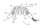
- An AWG 90 comprises an array 91 of waveguides disposed between a first star coupler 92 and a second star coupler 93 .
- the optical path length of the waveguides 91 increases monotonically by a constant value across the waveguide array. If the path lengths of the waveguides 91 do not increase by a constant value across the array, there will be cross-talk between output channels 94 when the AWG is operated as a demultiplexer.
- An AWG can be manufactured according to the present invention by first depositing a series of adjacent waveguides on a single substrate at a formation temperature below the melting point of the waveguide material.
- Post-formation optical analysis of the AWG can confirm the effective refractive index profile of the array 91 and detect any inhomogenities in the array that could potentially lead to signal cross-talk. It sometimes happens that non-uniformities in the deposition process produce a systematic variation in effective refractive index across the array of waveguides 91 .
- a tapered heater can be deposited across the width of the array such that the narrowest regions of the heater cover the waveguides which need to be trimmed to the greatest extent, and vice versa.
- FIG. 5 illustrates an example of such a heater in which a series of tapered heating elements 96 are deposited along the length of the waveguide array 91 , each element covering the width of the array 91 .
- the heating elements 96 are tapered to provide greater heating in the narrower sections. A heating current is then applied through contact pads 95 to the heating elements 96 to remove the inhomogenities by altering the effective refractive index profile of the waveguide array 91 .
- An alternative technique (not shown) of using heating elements to trim the waveguides 91 is to deposit separate heating elements over one or more selected waveguides within the array 91 and to anneal those waveguides separately without affecting the remaining waveguides in the array.
- the present invention allows waveguide structures to be produced in a more flexible and thus more cost effective manner by providing a post-formation process allowing the structures to be trimmed to requirements.
- An important advantage of the invention is that the methods can be used for the production of generic components that can be trimmed within broad parameters to suit specific requirements with little consideration of the specific use to which those components will ultimately be put.
Landscapes
- Physics & Mathematics (AREA)
- Engineering & Computer Science (AREA)
- Microelectronics & Electronic Packaging (AREA)
- General Physics & Mathematics (AREA)
- Optics & Photonics (AREA)
- Optical Modulation, Optical Deflection, Nonlinear Optics, Optical Demodulation, Optical Logic Elements (AREA)
- Optical Integrated Circuits (AREA)
Abstract
Description
Claims (31)
Priority Applications (1)
| Application Number | Priority Date | Filing Date | Title |
|---|---|---|---|
| US09/946,712 US6807349B2 (en) | 2001-09-04 | 2001-09-04 | Planer waveguide and method of formation |
Applications Claiming Priority (1)
| Application Number | Priority Date | Filing Date | Title |
|---|---|---|---|
| US09/946,712 US6807349B2 (en) | 2001-09-04 | 2001-09-04 | Planer waveguide and method of formation |
Publications (2)
| Publication Number | Publication Date |
|---|---|
| US20030044153A1 US20030044153A1 (en) | 2003-03-06 |
| US6807349B2 true US6807349B2 (en) | 2004-10-19 |
Family
ID=25484864
Family Applications (1)
| Application Number | Title | Priority Date | Filing Date |
|---|---|---|---|
| US09/946,712 Expired - Fee Related US6807349B2 (en) | 2001-09-04 | 2001-09-04 | Planer waveguide and method of formation |
Country Status (1)
| Country | Link |
|---|---|
| US (1) | US6807349B2 (en) |
Cited By (3)
| Publication number | Priority date | Publication date | Assignee | Title |
|---|---|---|---|---|
| US20030128927A1 (en) * | 2001-11-01 | 2003-07-10 | Kazumi Wada | Array waveguide grating |
| US20040017990A1 (en) * | 2002-07-29 | 2004-01-29 | Intel Corporation | Thermal optical switch apparatus and methods with enhanced thermal isolation |
| US20050213883A1 (en) * | 2001-10-09 | 2005-09-29 | Infinera Corporation | Method of optimizing optical channel signal demultiplexing in a monolithic receiver photonic integrated circuit (RxPIC) |
Families Citing this family (9)
| Publication number | Priority date | Publication date | Assignee | Title |
|---|---|---|---|---|
| US6705124B2 (en) * | 2001-06-04 | 2004-03-16 | Lightwave Microsystems Corporation | High-density plasma deposition process for fabricating a top clad for planar lightwave circuit devices |
| US20030033834A1 (en) * | 2001-08-17 | 2003-02-20 | Michael Bazylenko | Method of depositing a cladding layer |
| US20030068130A1 (en) * | 2001-10-09 | 2003-04-10 | Photon-X, Inc. | Dynamic gain-equalizing filter based on polymer optical waveguide gratings |
| US7050663B2 (en) * | 2001-10-17 | 2006-05-23 | Intel Corporation | Integrated optical circuit having an integrated arrayed waveguide grating (AWG) and optical amplifier(s) |
| US7024065B2 (en) * | 2002-07-09 | 2006-04-04 | Lucent Technologies Inc. | Optical waveguide device and method of manufacture therefor |
| KR102501643B1 (en) * | 2015-09-24 | 2023-02-20 | 삼성전자주식회사 | Optical device having high refractive index optical functional layer and method of fabricating the same |
| GB2546966B (en) * | 2016-01-21 | 2021-08-04 | Univ Southampton | Trimming optical device structures |
| CN109962770B (en) * | 2017-12-14 | 2024-03-12 | 科大国盾量子技术股份有限公司 | Silicon-based monolithic integrated quantum key distribution sender chip |
| GB201908145D0 (en) * | 2019-06-07 | 2019-07-24 | Univ Oxford Innovation Ltd | Optical device with tuneable optical properties |
Citations (4)
| Publication number | Priority date | Publication date | Assignee | Title |
|---|---|---|---|---|
| US4934774A (en) * | 1989-06-08 | 1990-06-19 | Northern Telecom Limited | Optical waveguide and method for its manufacture |
| US5117470A (en) * | 1990-02-26 | 1992-05-26 | Nippon Telegraph And Telephone Corporation | Guided-wave optical circuit and method for adjusting a characteristic thereof |
| US20020031319A1 (en) * | 2000-06-09 | 2002-03-14 | Shih-Yuan Wang | Method of fabricating microstructured optical fibers |
| US6522799B1 (en) * | 1999-03-18 | 2003-02-18 | The University Of Sydney | Optical planar waveguide device and method of fabrication |
-
2001
- 2001-09-04 US US09/946,712 patent/US6807349B2/en not_active Expired - Fee Related
Patent Citations (5)
| Publication number | Priority date | Publication date | Assignee | Title |
|---|---|---|---|---|
| US4934774A (en) * | 1989-06-08 | 1990-06-19 | Northern Telecom Limited | Optical waveguide and method for its manufacture |
| US5035916A (en) * | 1989-06-08 | 1991-07-30 | Northern Telecom Limited | Optical waveguide and method for its manufacture |
| US5117470A (en) * | 1990-02-26 | 1992-05-26 | Nippon Telegraph And Telephone Corporation | Guided-wave optical circuit and method for adjusting a characteristic thereof |
| US6522799B1 (en) * | 1999-03-18 | 2003-02-18 | The University Of Sydney | Optical planar waveguide device and method of fabrication |
| US20020031319A1 (en) * | 2000-06-09 | 2002-03-14 | Shih-Yuan Wang | Method of fabricating microstructured optical fibers |
Cited By (6)
| Publication number | Priority date | Publication date | Assignee | Title |
|---|---|---|---|---|
| US20050213883A1 (en) * | 2001-10-09 | 2005-09-29 | Infinera Corporation | Method of optimizing optical channel signal demultiplexing in a monolithic receiver photonic integrated circuit (RxPIC) |
| US7158699B2 (en) * | 2001-10-09 | 2007-01-02 | Infinera Corporation | Method of optimizing optical channel signal demultiplexing in a monolithic receiver photonic integrated circuit (RxPIC) |
| US20030128927A1 (en) * | 2001-11-01 | 2003-07-10 | Kazumi Wada | Array waveguide grating |
| US7043120B2 (en) * | 2001-11-01 | 2006-05-09 | Massachusetts Institute Of Technology | Array waveguide grating |
| US20040017990A1 (en) * | 2002-07-29 | 2004-01-29 | Intel Corporation | Thermal optical switch apparatus and methods with enhanced thermal isolation |
| US6895157B2 (en) * | 2002-07-29 | 2005-05-17 | Intel Corporation | Thermal optical switch apparatus and methods with enhanced thermal isolation |
Also Published As
| Publication number | Publication date |
|---|---|
| US20030044153A1 (en) | 2003-03-06 |
Similar Documents
| Publication | Publication Date | Title |
|---|---|---|
| US6807349B2 (en) | Planer waveguide and method of formation | |
| US6704487B2 (en) | Method and system for reducing dn/dt birefringence in a thermo-optic PLC device | |
| US7304799B2 (en) | Tunable optical filter with heater on a CTE-matched transparent substrate | |
| EP1936322A2 (en) | Interfermeter and its fabrication method | |
| WO2008047634A1 (en) | Thermo-optic phase shifter and method for producing the same | |
| US6553170B2 (en) | Method and system for a combination of high boron and low boron BPSG top clad fabrication process for a planar lightwave circuit | |
| US20020159698A1 (en) | Tunable filter | |
| JP2002303752A (en) | Optical waveguide and method for manufacturing the same | |
| US11662519B2 (en) | Optical waveguide tuning element | |
| WO2000057222A1 (en) | Waveguide structure and method of forming the waveguide structure | |
| US20020159700A1 (en) | Tunable filter | |
| JP2003050327A (en) | Optical waveguide device and method for manufacturing the same | |
| US6870967B2 (en) | Pretrimming of tunable finite response (FIR) filter | |
| JP2002098850A (en) | Non-birefringent passive optical components | |
| TWI357511B (en) | ||
| JP2002156539A (en) | Optical waveguide | |
| TW200405048A (en) | Polarization-insensitive planar lightwave circuits and method for fabricating the same | |
| JPH0659293A (en) | Tunable optical filter | |
| US20100092682A1 (en) | Method for Fabricating a Heater Capable of Adjusting Refractive Index of an Optical Waveguide | |
| JP4424455B2 (en) | Manufacturing method of optical waveguide circuit | |
| JP3880222B2 (en) | Temperature compensation material for temperature compensated planar optical waveguide component and temperature compensated planar optical waveguide component using the same | |
| JP3223959B2 (en) | Optical path length trimming method and apparatus in waveguide type optical circuit | |
| JP2006259104A (en) | Optical circuit and waveguide type optical variable attenuator | |
| US8098999B2 (en) | Multiple channel power monitor | |
| US6816635B2 (en) | Optical waveguide phase shifter |
Legal Events
| Date | Code | Title | Description |
|---|---|---|---|
| AS | Assignment |
Owner name: REDFERN INTEGRATED OPTICS PTY LTD., AUSTRALIA Free format text: ASSIGNMENT OF ASSIGNORS INTEREST;ASSIGNOR:BAZYLENKO, MICHAEL;REEL/FRAME:012338/0299 Effective date: 20011102 |
|
| AS | Assignment |
Owner name: TALLWOOD I, L.P., AS AGENT, CALIFORNIA Free format text: SECURITY INTEREST;ASSIGNOR:REDFERN INTEGRATED OPTICS PTY LTD;REEL/FRAME:020627/0079 Effective date: 20080215 |
|
| REMI | Maintenance fee reminder mailed | ||
| LAPS | Lapse for failure to pay maintenance fees | ||
| STCH | Information on status: patent discontinuation |
Free format text: PATENT EXPIRED DUE TO NONPAYMENT OF MAINTENANCE FEES UNDER 37 CFR 1.362 |
|
| FP | Lapsed due to failure to pay maintenance fee |
Effective date: 20081019 |