US6788036B1 - Method and system for current sharing among a plurality of power modules - Google Patents
Method and system for current sharing among a plurality of power modules Download PDFInfo
- Publication number
- US6788036B1 US6788036B1 US10/401,463 US40146303A US6788036B1 US 6788036 B1 US6788036 B1 US 6788036B1 US 40146303 A US40146303 A US 40146303A US 6788036 B1 US6788036 B1 US 6788036B1
- Authority
- US
- United States
- Prior art keywords
- signal
- current
- power
- output
- coupled
- Prior art date
- Legal status (The legal status is an assumption and is not a legal conclusion. Google has not performed a legal analysis and makes no representation as to the accuracy of the status listed.)
- Expired - Lifetime
Links
Images


Classifications
-
- H—ELECTRICITY
- H02—GENERATION; CONVERSION OR DISTRIBUTION OF ELECTRIC POWER
- H02J—ELECTRIC POWER NETWORKS; CIRCUIT ARRANGEMENTS OR SYSTEMS FOR SUPPLYING OR DISTRIBUTING ELECTRIC POWER; SYSTEMS FOR STORING ELECTRIC ENERGY
- H02J1/00—Circuit arrangements for DC mains or DC distribution networks
- H02J1/10—Parallel operation of DC sources
- H02J1/102—Parallel operation of DC sources being switching converters
-
- G—PHYSICS
- G05—CONTROLLING; REGULATING
- G05F—SYSTEMS FOR REGULATING ELECTRIC OR MAGNETIC VARIABLES
- G05F1/00—Automatic systems in which deviations of an electric quantity from one or more predetermined values are detected at the output of the system and fed back to a device within the system to restore the detected quantity to its predetermined value or values, i.e. retroactive systems
- G05F1/10—Regulating voltage or current
Definitions
- the present invention relates generally to power supplies, and more particularly, to current sharing and equalization techniques among multiple DC-to-DC and AC-to-DC power modules.
- the DC power supplies may be stand-alone power supplies or may be power modules designed for integration into larger power supplies or power storage.
- Power supply in this context conventionally refers to a voltage/current converter, not to the ultimate source of electric current such as a battery or generator.
- the multi-module power system can provide for failure recovery if one module ceases to operate.
- simply supplementing the design with additional power supplies or power modules may increase the total current capacity of a multi-module power system.
- Such power systems are used in telecommunications equipment and other equipment requiring a reliable source of power, e.g., matrix switches and industrial controllers.
- the total current delivered to a load from a power system having multiple power modules configured in parallel equals the sum of the currents delivered by each individual power module.
- the current supplied by each power module contributes to the total load current supplied by the power system. If one module delivers a greater amount of current, that module will also dissipate more power and therefore become hotter than the other power modules. Higher operating temperature normally yields reduced reliability of the overall power system. Therefore, there is a goal of evenly distributing the task of generating the total load current among parallel-connected power supplies or power modules.
- FIGS. 1A and 1B illustrate two different power system configurations, each using multiple power supplies.
- FIG. 1A illustrates a power system 10 having multiple power modules 100 , 101 , 102 , 103 configured in parallel supplying power to a load 40 .
- Each module accepts an input voltage V DD 20 and provides an output current I 0 , I 1 , I 2 , I 3 to a power system output node 30 .
- the sum of the individual module output currents is supplied to load 40 .
- the total load current I LOAD I 0 +I 1 +I 2 +I 3 results in a voltage V LOAD across the load referenced between output node 30 of power system 10 and a ground 50 .
- power system 10 will be unable to control and equalize the currents I 0 , I 1 , I 2 , I 3 supplied by respective modules 100 , 101 , 102 , 103 .
- each power module will deliver an equal amount of power. By evenly dividing the task of providing power among the power modules, no one power module will be driven to an extreme that may cause power conversion inefficiencies, power module degradation or premature power module failure.
- an external controller may be used to sense and adjust each module's current output.
- the power modules may be designed to communicate among each other and self regulate their output power. For example, a power system may be designed such that each module communicates its current output to other power modules and each module adjusts its output based on the received signal.
- Some power systems utilize a single wire or twisted pair configured as a shared bus to communicate the maximum current supplied by any one of the parallel-connected power modules.
- each of a plurality of power modules is connected to a shared bus.
- Each power module attempts to raise the voltage on the shared bus to a value indicative of the current supplied by that power module.
- the power module providing the greatest current to the load overrides the voltage provided by the other power modules.
- the voltage level on the shared bus therefore corresponds to a level indicating the current supplied by the power module providing the most current.
- FIG. 1B illustrates a power system having such a current-share bus.
- the input node 20 and output node 30 of the power system are equivalent to those previously described with reference to FIG. 1 A.
- each module 100 , 101 , 102 , 103 in the power system 10 of FIG. 1B communicates with the other modules by way of a current-share bus 200 .
- the current-share bus 200 may be a single wire providing a signal relative to a common ground of the power system 10 .
- each power module also monitors the shared bus to determine the maximum current supplied by any one of the power modules. If each power module is providing the same amount of current to the load, the voltage applied to the current-share bus set by each module is equal to the voltage monitored by each module from the shared bus. Any power module providing a level of current below that which is indicated on the current-share bus will detect that at least one module is providing more current and thus more power than it is providing. A module providing less current than that indicated on the shared bus will incrementally increase its output voltage, which in turn will increase the current supplied to the load, until the current supplied by the power module equals the current indicated on the current-share bus. In this way, each of a plurality of parallel power modules will increase its output current in an attempt to track the output current supplied by the module providing the most current.
- Each power module also monitors the output voltage supplied by the multi-module power system. As some power modules increase their current outputs, the total output voltage of the power system provided to the load may exceed the voltage demanded by the load. Each power module providing a current equal to the current indicated on the current-share bus will reduce its output current until the voltage provided to a load by the power system equals the desired voltage. With time, the power modules work in tandem to evenly distribute the current supplied by the power modules and to provide a regulated output voltage to the load. If the load's power demands change over time, the power modules track the changing demand by adjusting the current supplied by each module. If current sharing is operating properly, the resulting steady-state output currents I 0 , I 1 , I 2 , I 3 of each respective module 100 , 101 , 102 , 103 will be approximately equal to each another.
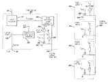
- FIGS. 2A and 2B show examples of power modules that include circuitry allowing the modules to communicate via a shared bus.
- FIG. 2A shows a power module 100 A that interfaces to a single-wire current-share bus that carries a shared analog signal representing an averaged signal.
- Power module 100 A includes a power regulator 110 and feedback circuitry including a current sensor 120 , a current-to-voltage converter 130 , interface circuitry 140 to the current-share bus 200 , a voltage error amplifier 150 A, and interface circuitry 160 to the power regulator 110 .
- Power regulator 110 generates an output current I OUTPUT .
- Power regulator 110 may be one of any of a number of power converter types, including for example, buck, boost, buck-boost or other current-providing power module well known in the art.
- Feedback circuitry in the power module separate from any feedback circuitry within power regulator 110 , provides a feedback voltage V FEEDBACK to power regulator 110 .
- Power regulator 110 contains its own feedback circuitry (not shown) to control the output voltage of the power regulator.
- the feedback voltage V FEEDBACK alters the internal feedback circuitry of the power regulator 110 to provide current sharing, as will be further described below.
- Current sensor 120 monitors the output of the power regulator 110 and provides a signal to current-to-voltage converter 130 indicative of the output current I OUTPUT .
- Current-to-voltage converter 130 translates the signal indicative of the output current to an analog voltage level. This voltage level is coupled to one input of voltage error amplifier 150 A.
- the voltage level is also passed through a resister 140 , which is connected to current-share bus 200 .
- Resistor 140 in combination with similarly situated resistors of other power modules (not shown) average the voltage levels supplied by each power module.
- the averaged voltage on current-share bus 200 represents the average current supplied by all of the power modules connected to current-share bus 200 .
- the voltage residing on current-share bus 200 is supplied as a second input to voltage error amplifier 150 A.
- the voltage error amplifier 150 A determines the difference between the output voltage of converter 130 and the average voltage level provided by current-share bus 200 . If the difference is positive, the output current I OUTPUT is greater than the average current of the power modules. To equalize the output currents of each power module, voltage error amplifier 150 A and resistor 160 generate a feedback voltage V FEEDBACK that directs power regulator 110 to adjust the output current. Power regulator 110 uses this feedback voltage V FEEDBACK to decrease the output voltage of the regulator.
- the output current I OUTPUT is less than the average current of the power modules.
- voltage error amplifier 150 A will increase the feedback voltage V FEEDBACK provided through resistor 160 .
- power regulator 110 increases the output voltage, which in turn increases the output current I OUTPUT .
- current-share bus 200 shorts to ground, each power module will drive its output voltage towards zero volts.
- FIG. 2B shows another power module 100 B that interfaces to a single-wire current-share bus that also carries a shared analog signal.
- a plurality of parallel-connected power modules connected to a common current-share bus 200 such as the power-module 100 B shown in FIG. 2B, results in a voltage level on current-share bus 200 that represents the maximum current provided by any one of the power modules.
- the design of power module 100 B functions substantially as described above with reference to power module 100 A in FIG. 2A except, for example, the interface to current-share bus 200 and associated circuitry is modified.
- the voltage level provided by current-to-voltage converter 130 is passed through diode 170 , which pulls up current-share bus 200 to at least the output voltage level of converter 130 , assuming the voltage drop across diode 170 is negligible. If any one of the other power modules pulls current-share bus 200 to a value higher than the voltage level provided by converter 130 of module 100 B, diode 170 will be reversed biased and current-share bus 200 will be unaffected by this power module. As a result, current-share bus 200 is held to the highest value produced by the power module generating the greatest output current.
- Error amplifier 150 B has two input signals: (1) a negative input providing a voltage level offset by V OFFSET ; and (2) a positive input providing the maximum voltage level sent to current-share bus 200 by all of the power modules.
- the first input signal is equal to the output voltage level of converter 130 increased by an offset voltage V OFFSET .
- the offset in voltage helps to stabilize the feedback loop by helping to set a clear master, i.e., a power module that produces slightly more current than the other modules. If the resulting offset voltage level at the negative input is greater than the maximum voltage level riding on current-share bus 200 , voltage error amplifier 150 B provides a lower feedback signal V FEEDBACK .
- diode 190 prevents passing of this feedback signal to power regulator 110 and the output voltage of regulator 110 remains unchanged.
- voltage error amplifier 150 B provides a higher feedback signal V FEEDBACK through the serially connected diode 190 and resistor 160 thereby increasing the output voltage and in turn the output current I OUTPUT of power regulator 110 .
- a system using an analog shared bus communicating an amplitude signal is susceptible to line noise on the bus.
- Noise can be generated by sources within the power system itself or can be generated by energy radiating from the load or neighboring electronic circuitry.
- Noise on the current-share bus may erroneously drive the power modules to inaccurate and unpredictable output currents.
- each power module might have a slightly different ground reference point. If a first power module has a lower ground reference than another power module, a voltage provided to the shared bus by the second power module will appear to the first power module as representing a larger current than actually exists.
- parasitic resistances in the power module circuitry may reduce the actual voltage supplied to the current-share bus. Thus, the voltage supplied to the current-share bus by a power module may not accurately indicate the supplied output current by a power module.
- methods and apparatus are provided for current sharing and equalization among a plurality of power modules configured in a parallel arrangement in a power system.
- a method of sharing current among a plurality of power modules includes sensing of a characteristic of an output power signal of at least one of the plurality of power modules and providing a first signal having a pulse width corresponding to the sensed characteristic.
- the first signal is imparted onto a current share bus coupled to each of the plurality of power modules if the first signal has a pulse width greater than corresponding first signals of other power modules coupled to the current share bus, whereupon one of the first signals from the plurality of power modules having greatest pulse width is imparted onto the current share bus as a second signal.
- a phase difference between the first signal and the second signal is detected and a feedback signal is provided to the at least one power module in response to the detected phase difference. The feedback signal thereby controls the at least one power module to regulate the output power signal.
- a power module for operation with a plurality of like power modules connected together to provide a common output.
- the power module includes a power regulator providing an output power signal on a corresponding output terminal, and a bus interface adapted to communicate with a current share bus that is connected in like manner to each of the other power modules.
- the power module further includes a feedback loop adapted to sense the current level of the output power signal and provide a feedback signal to the power regulator in response thereto. The feedback signal thereby controls the power regulator to regulate the output power signal.
- the feedback loop further includes a converter adapted to provide a first signal having a pulse width corresponding to the sensed current level, and an error controller adapted to detect a phase difference between the first signal and a second signal received through the bus interface from the current share bus.
- the feedback loop imparts the first signal onto the current share bus if the first signal has a pulse width greater than corresponding first signals of the other power modules communicating with the current share bus, whereupon the first signal becomes the second signal.
- FIGS. 1A and 1B illustrate in block diagram form known power systems having multiple power modules configured in parallel to supply a load.
- FIGS. 2A and 2B illustrate in block diagram form known power modules that communicate via a bus.
- FIGS. 3A and 3B illustrate graphically a translation of a current signal to an amplitude signal of known power modules.
- FIGS. 3C and 3D illustrate a translation of a current signal to a time based pulse signal according to some embodiments of the present invention.
- FIG. 4A shows a block diagram of a power module with interface circuitry to connect to a binary level current-share bus according to some embodiments of the present invention.
- FIG. 4B shows schematically the binary level current-share bus interface circuitry of multiple power modules according to some embodiments of the present invention.
- FIG. 4C shows an example of timing diagrams of inputs and outputs of multiple power modules connected to a binary level current-share bus according to some embodiments of the present invention.
- FIG. 5A shows a block diagram of an embodiment of a current-to-pulse width converter according to some embodiments of the present invention.
- FIG. 5B shows schematically an embodiment of a signal generator according to some embodiments of the present invention.
- FIG. 5C shows timing diagrams of internal, input and output signals of a current-to-pulse width converter according to some embodiments of the present invention.
- FIG. 6 shows a block diagram of a phase difference error controller according to some embodiments of the present invention.
- FIGS. 7A and 7B show schematically two embodiments of a phase detector according to some embodiments of the present invention.
- FIGS. 7C and 7D show timing diagrams for a phase detector according to some embodiments of the present invention.
- FIG. 8 shows schematically a loop filter according to some embodiments of the present invention.
- FIGS. 1 through 8 of the drawings include symbolic representations used by those skilled in the art of power supply design that are most effective at conveying the teachings and discoveries to others skilled in the art.
- FIGS. 3A and 3B illustrate graphically one translation of a current signal to an amplitude signal utilized by known power modules of FIGS. 2A and 2B.
- current-to-voltage converter 130 (of FIGS. 2A and 2B) translates the current I OUTPUT to an output voltage level V 1 .
- FIG. 3A shows the one-to-one mapping of a current value to a voltage value.
- FIG. 3B shows the output voltage V 1 of converter 130 over time where the input to converter 130 is the result of a constant output current value I OUTPUT . If the output current changes with time, the output of converter 130 also changes to track the current changes.
- FIGS. 3C and 3D illustrate graphically a translation of a current signal to a time pulse signal in accordance with some embodiments of the present invention.
- a current-to-pulse width converter 330 (of FIG. 4A) translates the output I OUTPUT into an output pulse with period T 1 .
- FIG. 3C shows the one-to-one mapping of a current value provided by a power module to a pulse having a pulse width of value T 1 .
- FIG. 3D shows the output of converter 330 as a pulse having a fixed amplitude V p for a variable period T 1 and an amplitude of zero volts outside period T 1 .
- the output of converter 330 represents a single current value over a system synchronization period (e.g., T SYNC ). Each occurrence of a synchronization signal leads to the generation of a new pulse. If the output current is unchanged, the sequence of pulses will appear as a rectangular wave. Output of converter 330 represents the instantaneous current value at one point of the system period. The resulting pulse may be used to induce a time based pulse signal on a binary level current-share bus 200 .
- a binary level current-share bus 200 operates at two values, e.g., V P volts and zero volts. As a result, the duration between low-high and high-low transitions on binary current-share bus 200 represents an output current level of a power module.
- FIG. 4A shows a block diagram of a power module with interface circuitry for connecting to a binary level current-share bus 200 according to embodiments of the present invention.
- the current-to-voltage converter 130 of FIG. 2B is replaced with a current-to-pulse width converter 330 .
- converter 330 Based on the sensed current provided by current sensor 120 , converter 330 generates a pulse V P (t) having a pulse width indicative of the output current I OUTPUT generated by power regulator 110 .
- the pulse is used both as a gate control to a switch S 1 340 and as an input to a delay and inverter circuit 360 .
- switch S 1 340 When high, the pulse voltage V P (t) is applied to switch S 1 340 as V GATE , which enables switch S 1 340 to conduction. When V P (t) is low, the voltage V GATE inhibits switch S 1 340 from conducting. When enabled or closed, switch S 1 340 shunts current-share bus 200 to a common ground 500 , thereby pulling current-share bus 200 to a low level for at least the duration of the width of the pulse V P (t). If switch S 1 340 of all power modules is open, there is no electrical path to ground 500 . Resistor 345 connected to a high voltage thus pulls bus 200 to the high voltage since there is no electrical path to ground 500 . Switch S 1 340 may be any suitable switch well known in the art. FIG.
- FIG. 4A shows an enhanced mode MOSFET for switch S 1 with its drain coupled to both bus 200 and pull-up resistor 345 , its source coupled to common ground 500 , its substrate region (body) coupled to the source, and its gate coupled to the output of converter 330 .
- pull-up resistor 345 may be replaced by a current source.
- the output of converter 330 is also provided to delay and invert circuitry (inverter) 360 .
- Delay circuitry 360 aids in stabilizing the feedback control loop. The leading edge of the pulse is not necessarily delayed, however, the delay circuitry does delay the trailing edge of the pulse by a predetermined amount ⁇ , thereby potentially increasing the total pulse width by the amount ⁇ . Circuitry 360 also inverts the pulse such that the delayed and inverted pulse is comparable to the pulse received from current-share bus 200 . Alternatively; the signal from the bus 200 may be inverted to provide comparable signals.
- phase difference error controller 350 The output of circuitry 360 is provided as input P 1 to a phase difference error controller 350 .
- the phase difference error controller 350 also accepts a second input P 2 , which represents the signal provided by current-share bus 200 .
- controller 350 determines whether feedback voltage V FEEDBACK should be adjusted up or down. Controller 350 may then adjust feedback voltage V FEEDBACK provided to power regulator 110 . Power regulator 110 references V FEEDBACK to increase the output voltage.
- FIG. 4B shows schematically the binary level current-share bus interface circuitry of multiple power modules 300 - 303 according to some embodiments of the present invention.
- the embodiment shows a wired-OR configuration. If the gate voltage for switch S 1 340 of each power module 300 - 303 disables the switch S 1 , pull-up resistor 345 pulls current-share bus 200 to a high value. If any of switches S 1 340 is closed, current-share bus 200 will have a direct path to common ground 500 , thereby setting a low value on current-share bus 200 . In sum, if any one of the switches S 1 is on, bus 200 is low and bus 200 is high only if all of the switches are off. Though FIG. 4B shows four power modules, any number of power modules may be connected in the wired-OR (parallel) fashion shown. Additionally, only one of the modules need contain a pull-up resistor 345 .
- the interface circuitry may be reversed such that current-share bus 200 carries an inverted pulse to the one described above.
- a switch connects the bus to a high value when enabled. When disabled, the switch allows a pull-down resistor to hold the bus 200 low if no other power modules had an enabled switch.
- FIG. 4C shows timing diagrams of one example of outputs from multiple power modules that are connected to a binary level current-share bus according to some embodiments of the present invention.
- Waveform (A) shows a periodic synchronization pulse SYNC.
- the power modules may use the synchronization pulse to initiate the pulse generated by converter 330 .
- the SYNC signal may be the leading negative slope of the signal on the current-share bus.
- the controller running with the highest internal clock controls the share bus frequency and additional external circuitry to generate a synchronization signal may be discarded.
- one power module becomes the master, for example, the power module with the highest free-running frequency, or the first module to have an internal time expire.
- the master synchronizes all of the modules attached to the single-wire shared bus.
- the master supplies a signal to the bus from which each of the modules acquire timing.
- the falling edge of the signal on the shared bus may be considered a synchronization mark.
- the master may hold the shared bus low for a minimum duration to allow each of the attached power modules the opportunity to detect the falling edge transition.
- each module On detecting the falling edge on the shared bus signal, each module holds the shared bus low for a predetermined length of time.
- the bus While the bus is held low by the modules, the bus provides a low signal to all modules. Even when only one module is holding the bus low, all of the modules will detect a low signal on the bus. Once the last module has released the bus, the signal on the bus transitions from a low to a high value. This rising edge is then used to achieve the current share function. Each of the modules detects this low-to-high transition and may use the timing of this transition in relation to the timing of its release of the bus to adjust internal parameters for module self regulation.
- Waveform (B) shows the voltage V P that is generated by converter 330 of power module 0 and is applied to the gate of switch S 1 340 . Over time, the signal V P (t) appears as a sequence of pulses having pulse width T 0 . Pulse width T 0 may change from pulse to pulse as the output current changes.
- Waveform (C) shows the resulting signal after the gate voltage V GATE passes through delay and invert circuitry 360 . The trailing edge of the pulse is delayed by a predetermined amount ⁇ and the entire signal is inverted. The resulting pulse has a pulse width of T 0 + ⁇ if just the trailing edge is delayed and the leading edge is not delayed.
- waveforms (D), (F) and (H) show exemplary voltages V P generated by the converter 330 of power modules 1 , 2 and 3 , respectively. Over time, the voltages V P appear as a sequence of pulses having pulse widths T 1 , T 2 and T 3 .
- Waveforms (E), (G) and (I) show the resulting signal after the voltages V P pass through delay and invert circuitry 360 . Again, the trailing edges of the pulses are delayed by a predetermined amount ⁇ and each signal is inverted. The resulting negative pulses have respective pulse widths of T 1 + ⁇ , T 2 + ⁇ and T 3 + ⁇ .
- Waveform (J) shows an example of a signal imposed on current-share bus 200 by the combination of the example pulses generated by the power modules.
- the duration T MAX of the pulse on current-share bus 200 has a duration that is equal to the maximum of T 0 , T 1 , T 2 and T 3 .
- the pulse generated by power module 1 is longer than each of the other pulses generated by the remaining power modules.
- the voltage V P (t) enables the switch 340 of power module 1 for the duration of the pulse width T 1 .
- FIG. 5A shows a block diagram of an embodiment of a current-to-pulse width converter 330 of FIG. 4A according to some embodiments of the present invention.
- Current-to-pulse width converter 330 incorporates a signal generator 332 , an amplifier 334 and a comparator 336 .
- the converter 330 has an input for a synchronization pulse SYNC 331 , an input for a signal from a current sensor 120 , and an output V P (t).
- the signal generator 332 accepts a SYNC signal 331 , which is used to synchronize the generation of pulses among multiple power modules.
- Signal generator 332 provides a periodic one-to-one signal V S (t). For example, a saw-tooth signal may be used. Although saw-tooth signals provide a linear one-to-one signal over a period of one cycle, a linear signal is not necessary.
- the output of signal generator 332 is coupled to a first input of comparator 336 .
- Amplifier 334 connected in parallel to signal generator 332 , accepts a potential V R (t), which is the potential across a resistor R of current sensor 120 and is indicative of the current provided by power regulator 110 .
- the output V A (t) of the amplifier 334 is a scaled representation of the output current I OUTPUT and provides a second input to comparator 336 .
- Comparator 336 generates a signal V P (t) that is low while V S (t) is lower than V A (t) and is high while V S (t) is greater than V A (t).
- FIG. 5B shows an embodiment of a signal generator 332 according to some embodiments of the present invention.
- Signal generator 332 has a charging capacitor C S coupled to a low voltage potential, e.g., common ground 500 , coupled in series with a pull-up resistor R S and in parallel to switch S 2 .
- One end of the pull-up resistor R S is coupled to capacitor C S and the other end is coupled to a high voltage 20 , e.g., V DD .
- Switch S 2 may be any suitable switch, e.g., a bipolar transistor, as shown.
- Signal generator 332 charges capacitor C S while switch S 2 is open thereby providing an increasing voltage to output V S (t).
- FIG. 5C shows various waveforms related to the exemplary circuitry shown in FIGS. 5A and 5B.
- Waveforms (A) and (B) show a SYNC pulse and its inverse, respectively.
- Waveform (C) shows V S (t) generated by signal generator circuitry 332 of FIG. 5 B. The saw-tooth like pattern increases gradually as switch S 2 is open and capacitor C S charges. The signal then falls to zero when switch S 2 closes as a result of the SYNC signal going low.
- Waveform (D) shows a signal V A (t), which is a scaled version of current sensor signal V R (t) and whose amplitude is indicative of the instantaneous output current I OUTPUT .
- Waveform (E) overlaps waveforms (C) and (D) to illustrate the points at which V S (t) of waveform (C) intersects with V A (t) waveform (D).
- Waveform (F) shows V P (t), which is applied to the gate of switch S 1 340 of FIG. 4 A.
- the signal V P (t) is high when V S (t) is lower than V A (t) and low when V S (t) is greater than V A (t).
- the resulting pulse V P (t) has a pulse width that is indicative of the output current I OUTPUT during the present period.
- the output V P (t) of current-to-pulse width converter 330 passes through a delay and invert circuit 360 , which in turn provides a first input P 1 to phase difference error controller 350 .
- a second input P 2 to controller 350 is provided by current-share bus 200 .
- the controller 350 generates a feedback voltage V FEEDBACK , which is used by the power regulator 110 to adjust the overall output voltage of power module 300 .
- FIG. 6 shows a block diagram of a phase difference error controller 350 according to some embodiments of the present invention.
- Phase difference error controller 350 has a phase comparator 400 coupled to two inputs P 1 and P 2 , a loop filter 450 accepting outputs from phase comparator 400 , and a current sink 480 accepting an output from loop filter 450 .
- phase comparator 400 After comparing the trailing edges of P 1 and P 2 , phase comparator 400 generates either an UP signal or a DOWN signal.
- the UP signal indicates that the output current I OUTPUT is below a desired level.
- the DOWN signal indicates that the output current I OUTPUT is above the desired level.
- Loop filter 450 may be used to convert the UP and DOWN signals to shape the loop gain of the current share feedback loop and to provide a control voltage V LF OUT .
- the loop filter output voltage V LF OUT is used to control current sink 480 .
- current sink 480 draws an amount of current I SINK from a voltage divider network with the power regulator 110 .
- the voltage divider comprised of resistors R FB1 and R FB2 , may be incorporated within power regulator 110 or may be placed between controller 350 and regulator 110 .
- the resistors R FB1 and R FB2 sense the output voltage V LOAD Of the power regulator 110 so that the feedback voltage V FEEDBACK corresponds to the output voltage V LOAD .
- phase difference error controller 350 provides a feedback voltage V FEEDBACK that tends to drive the output current of power module 300 to a value indicated on bus 200 .
- FIGS. 7A and 7B show schematically two embodiments of a phase comparator according to some embodiments of the present invention.
- the two inputs P 1 and P 2 of phase comparator 400 A are inputs of an exclusive-OR gate 402 .
- the output of XOR gate 402 is provided to two AND gates 404 and 406 .
- Input signal P 1 is also an input to AND gate 404 , which provides an UP signal output of phase comparator 400 A.
- input signal P 2 is also an input to AND gate 406 , which provides a DOWN signal output of phase comparator 400 A.
- the XOR and AND gates provide an UP signal while P 1 is HIGH and P 2 is LOW.
- the gates provide a DOWN signal while P 2 is HIGH and P 1 is LOW.
- FIG. 7B shows another embodiment of a phase comparator 400 .
- Phase comparator 400 B accepts inputs P 1 and P 2 having leading edges that are not necessarily coincidental.
- the first input P 1 is used to clock a first D flip-flop 410 having its D input set to logic 1.
- logic 1 is represented by voltage level of 5 volts.
- the Q output of flip-flop 410 is used as an input to an AND gate 414 and to a NAND gate 412 .
- the negative Q output of 410 is used as an input to an AND gate 416 .
- the second input P 2 is used to clock a second D flip-flop 420 having its D input set to logic 1.
- the Q output of flip-flop 420 is used as an input to AND gate 416 and to NAND gate 412 .
- the negative Q output of flip-flop 420 is used as an input to AND gate 414 .
- AND gate 414 provides an UP pulse when the positive slope of P 1 is leading the positive slope of P 2 .
- AND gate 416 provides a DOWN pulse when the positive slope of P 2 is leading the positive slope of P 1 .
- Both the UP and DOWN signals are reset by NAND gate 412 feeding a clear signal to both flip-flops 410 and 420 .
- FIGS. 7C and 7D show timing diagrams related to a phase detector according to some embodiments of the present invention.
- FIG. 7C illustrates a power module that is providing a current below that which is provided by another power module as indicated on bus 200 .
- Waveform (A) shows signal V P (t) that is indicative of the power modules delivered output current I OUTPUT .
- Waveform (B) shows the first input P 1 to phase comparator 400 .
- P 1 is the delayed and inverted signal provided by circuitry 360 .
- P 1 has a duration of T 0 + ⁇ .
- Waveform (C) shows the second input P 2 to phase comparator 400 .
- P 2 has a duration of T MAX .
- FIG. 7D illustrates the timing of the power module that is determining the pulse width on bus 200 , i.e., the master.
- Waveform (A) shows signal V P (t) that indicates the power modules delivered output current I OUTPUT
- Waveform (B) shows the first input P 1 to phase comparator 400 .
- P 1 is the delayed and inverted signal provided by circuitry 360 .
- P 1 has a duration of T 1 + ⁇ .
- Waveform (C) shows the second input P 2 to phase comparator 400 .
- FIG. 8 shows schematically a loop filter according to some embodiments of the present invention.
- Loop filter 450 includes a switchable current source S 3 coupled to a power source, e.g., V DD , and to a center node.
- Loop filter 450 also includes a second switchable current source S 4 coupled between the center node and a common ground.
- a loop filter resistor R LF and a loop filter capacitor C LF are coupled in series between the center node and the common ground in parallel to S 4 and a zener diode DZ also coupled between the center node and ground.
- the center node is provided as the output V LF OUT Of loop filter 450 .
- Loop filter capacitor C LF holds a charge to indicate the proper feedback signal.
- switchable current source S 3 When loop filter 450 receives an UP pulse, switchable current source S 3 temporarily injects current into the center node to charge C LF and raise the output voltage V LF OUT .
- switchable current source S 4 When loop filter 450 receives a DOWN pulse, switchable current source S 4 temporarily drains current from the center node, thereby removing charge from C LF and lowering the output voltage V LF OUT
- the zener diode DZ is used to limit the maximum output voltage V LF OUT .
- the output voltage V LF OUT is limited such to limit the maximum rise of the output voltage provided by the power regulator 110 to a range from 5 to 10%.
Landscapes
- Engineering & Computer Science (AREA)
- Power Engineering (AREA)
- Physics & Mathematics (AREA)
- Electromagnetism (AREA)
- General Physics & Mathematics (AREA)
- Radar, Positioning & Navigation (AREA)
- Automation & Control Theory (AREA)
- Inverter Devices (AREA)
- Dc-Dc Converters (AREA)
- Power Conversion In General (AREA)
- Supply And Distribution Of Alternating Current (AREA)
Abstract
Description

Claims (34)
Priority Applications (6)
| Application Number | Priority Date | Filing Date | Title |
|---|---|---|---|
| US10/401,463 US6788036B1 (en) | 2003-03-28 | 2003-03-28 | Method and system for current sharing among a plurality of power modules |
| EP04759645A EP1618442B1 (en) | 2003-03-28 | 2004-03-17 | Method and system for current sharing among a plurality of power modules |
| AT04759645T ATE539394T1 (en) | 2003-03-28 | 2004-03-17 | METHOD AND SYSTEM FOR POWER SHARING BETWEEN SEVERAL POWER MODULES |
| PCT/US2004/008246 WO2004095670A2 (en) | 2003-03-28 | 2004-03-17 | Method and system for current sharing among a plurality of power modules |
| CNB2004800000059A CN100511076C (en) | 2003-03-28 | 2004-03-17 | Method and system for implementing current sharing among multiple power modules |
| KR1020047007812A KR100768926B1 (en) | 2003-03-28 | 2004-03-17 | Method and system for current sharing among a plurality of power modules |
Applications Claiming Priority (1)
| Application Number | Priority Date | Filing Date | Title |
|---|---|---|---|
| US10/401,463 US6788036B1 (en) | 2003-03-28 | 2003-03-28 | Method and system for current sharing among a plurality of power modules |
Publications (1)
| Publication Number | Publication Date |
|---|---|
| US6788036B1 true US6788036B1 (en) | 2004-09-07 |
Family
ID=32927335
Family Applications (1)
| Application Number | Title | Priority Date | Filing Date |
|---|---|---|---|
| US10/401,463 Expired - Lifetime US6788036B1 (en) | 2003-03-28 | 2003-03-28 | Method and system for current sharing among a plurality of power modules |
Country Status (6)
| Country | Link |
|---|---|
| US (1) | US6788036B1 (en) |
| EP (1) | EP1618442B1 (en) |
| KR (1) | KR100768926B1 (en) |
| CN (1) | CN100511076C (en) |
| AT (1) | ATE539394T1 (en) |
| WO (1) | WO2004095670A2 (en) |
Cited By (24)
| Publication number | Priority date | Publication date | Assignee | Title |
|---|---|---|---|---|
| US20060158159A1 (en) * | 2005-01-19 | 2006-07-20 | Fujitsu Limited | Multiphase DC-DC converter |
| US7142046B1 (en) * | 2004-05-14 | 2006-11-28 | Fairchild Semiconductor Corporation | Current sharing using gate modulated diodes |
| US20060279269A1 (en) * | 2005-06-08 | 2006-12-14 | Ta-Yung Yang | Voltage-regulator and power supply having current sharing circuit |
| US20060279971A1 (en) * | 2005-06-08 | 2006-12-14 | Ta-Yung Yang | Power supply with current-sharing control and current-sharing method thereof |
| US20070050655A1 (en) * | 2005-08-23 | 2007-03-01 | Linear Technology Corporation | Single-wire sequencing technique |
| US20070091658A1 (en) * | 2005-10-21 | 2007-04-26 | Texas Instruments Incorporated | System and method for distributing module phase information |
| US20080174179A1 (en) * | 2007-01-18 | 2008-07-24 | Fujitsu Limited | Power supply device and method of supplying power supply voltage to load device |
| CN100414807C (en) * | 2005-01-21 | 2008-08-27 | 广西新未来信息产业股份有限公司 | Current-sharing control method and system for parallel modular inverse power supply |
| US20080309300A1 (en) * | 2007-06-12 | 2008-12-18 | Analog Devices, Inc. | Digital current share bus interface |
| US20090067199A1 (en) * | 2003-12-22 | 2009-03-12 | Koninklijke Philips Electronic, N.V. | Switched mode power supply |
| US7518264B1 (en) | 2008-05-29 | 2009-04-14 | International Business Machines Corporation | Digital current share method for power supplies in parallel |
| WO2010112094A1 (en) * | 2009-04-01 | 2010-10-07 | Telefonaktiebolaget Lm Ericsson (Publ) | Current share configuration in a power converter system |
| US20110001359A1 (en) * | 2009-07-03 | 2011-01-06 | Samsung Electro-Mechanics Co., Ltd. | Load sharing device and parallel power supply therewith |
| US20110018354A1 (en) * | 2007-09-11 | 2011-01-27 | Ching Hsiung Liu | Power System And Control Method Thereof |
| CN101282076B (en) * | 2007-03-29 | 2012-10-10 | 英特赛尔美国股份有限公司 | Multi-module current sharing scheme |
| EP2477296A4 (en) * | 2009-10-14 | 2013-05-01 | Zte Corp | AC POWER CURRENT SHARING METHOD AND APPARATUS THEREOF |
| US20140229755A1 (en) * | 2013-02-11 | 2014-08-14 | Microchip Technology Incorporated | Pulse width modulation load share bus |
| US20140300192A1 (en) * | 2011-06-27 | 2014-10-09 | Les Price | Power Supply |
| US9112411B2 (en) | 2012-04-25 | 2015-08-18 | Korea Institute Of Energy Research | Apparatus and method for controlling a plurality of power converting modules and apparatus and method for analyzing power quantity imbalance |
| EP2190094A3 (en) * | 2008-11-20 | 2015-12-09 | Siemens Schweiz AG | Method for providing electricity to the consumer in a bus and preswitching device |
| EP3016262A4 (en) * | 2013-07-29 | 2017-04-05 | ZTE Corporation | Rectifier mixed insertion system with different power, and energy saving implementation method and device therefor |
| CN114678858A (en) * | 2022-05-26 | 2022-06-28 | 安徽金屹能源发展有限公司 | Multi-group power supply parallel current-sharing circuit |
| CN117713530A (en) * | 2023-12-15 | 2024-03-15 | 上海军陶科技股份有限公司 | A multi-module synchronous start circuit |
| US12040641B2 (en) | 2021-06-22 | 2024-07-16 | Appleton Grp Llc | Systems and methods for situational suppression of overcurrent protection |
Families Citing this family (6)
| Publication number | Priority date | Publication date | Assignee | Title |
|---|---|---|---|---|
| CN101872972B (en) * | 2009-04-21 | 2013-04-10 | 陈金恩 | Power supply device for automobile fuse testing bench |
| US20180181181A1 (en) * | 2016-12-28 | 2018-06-28 | Hamilton Sundstrand Corporation | Differential current monitoring of multiple circuits |
| BE1026933B1 (en) * | 2018-12-28 | 2020-07-28 | Sofics Bvba | Driver for a common bus, in particular a LIN bus |
| CN111342444B (en) * | 2020-04-03 | 2024-03-19 | 西安清泰科新能源技术有限责任公司 | Switching ripple circulation suppression device and method for DC power supply system |
| KR102942698B1 (en) * | 2020-04-07 | 2026-03-23 | 엘지이노텍 주식회사 | Load sharing controller |
| KR102566878B1 (en) | 2022-10-07 | 2023-08-14 | 한화시스템 주식회사 | Power supply system for performing load-sharing functions |
Citations (21)
| Publication number | Priority date | Publication date | Assignee | Title |
|---|---|---|---|---|
| US3660672A (en) | 1971-02-25 | 1972-05-02 | Pioneer Magnetics Inc | Power supply dual output |
| US4194147A (en) | 1977-12-05 | 1980-03-18 | Burr-Brown Research Corporation | Parallel connected switching regulator system |
| US4538073A (en) | 1983-05-09 | 1985-08-27 | Convergent Technologies, Inc. | Modular power supply system |
| US4538101A (en) | 1982-06-04 | 1985-08-27 | Nippon Chemi-Con Corporation | Power supply device |
| US4616142A (en) * | 1984-12-31 | 1986-10-07 | Sundstrand Corporation | Method of operating parallel-connected semiconductor switch elements |
| US4622627A (en) | 1984-02-16 | 1986-11-11 | Theta-J Corporation | Switching electrical power supply utilizing miniature inductors integrally in a PCB |
| US5053920A (en) | 1989-06-09 | 1991-10-01 | Digital Equipment Corporation | Integrated power conversion |
| US5073848A (en) | 1990-11-21 | 1991-12-17 | General Electric Company | Power distribution system |
| US5377090A (en) | 1993-01-19 | 1994-12-27 | Martin Marietta Corporation | Pulsed power converter with multiple output voltages |
| US5481140A (en) | 1992-03-10 | 1996-01-02 | Mitsubishi Denki Kabushiki Kaisha | Demand control apparatus and power distribution control system |
| US5883797A (en) * | 1997-06-30 | 1999-03-16 | Power Trends, Inc. | Parallel path power supply |
| US5990669A (en) | 1997-12-15 | 1999-11-23 | Dell Usa, L.P. | Voltage supply regulation using master/slave timer circuit modulation |
| US6191566B1 (en) | 1999-08-26 | 2001-02-20 | Lucent Technologies Inc. | Board mountable power supply module with multi-function control pin |
| US6211579B1 (en) | 1999-09-29 | 2001-04-03 | Lucent Technologies, Inc. | Multiple output converter having a low power dissipation cross regulation compensation circuit |
| US20010033152A1 (en) | 2000-01-27 | 2001-10-25 | William Pohlman | Apparatus for providing regulated power to an integrated circuit |
| US20020073347A1 (en) | 2000-10-16 | 2002-06-13 | Stmicroelectronics S.R.I. | Managing system and synchronization method for a plurality of VRM-type modules |
| US6421259B1 (en) | 2000-12-28 | 2002-07-16 | International Business Machines Corporation | Modular DC distribution system for providing flexible power conversion scalability within a power backplane between an AC source and low voltage DC outputs |
| US20030122429A1 (en) | 2001-12-28 | 2003-07-03 | Zhang Kevin X. | Method and apparatus for providing multiple supply voltages for a processor |
| US20030142513A1 (en) | 2002-01-31 | 2003-07-31 | Patrizio Vinciarelli | Factorized power architecture with point of load sine amplitude converters |
| US20030201761A1 (en) | 2002-03-29 | 2003-10-30 | Intersil Americas Inc., State Of Incorporation: Delaware | Method and circuit for scaling and balancing input and output currents in a multi-phase DC-DC converter using different input voltages |
| US20040027101A1 (en) | 2002-08-08 | 2004-02-12 | Patrizio Vinciarelli | Buck-boost DC-DC switching power conversion |
Family Cites Families (8)
| Publication number | Priority date | Publication date | Assignee | Title |
|---|---|---|---|---|
| US4092712A (en) * | 1977-05-27 | 1978-05-30 | The United States Of America As Represented By The Administrator Of The National Aeronautics And Space Administration | Regulated high efficiency, lightweight capacitor-diode multiplier dc to dc converter |
| DE2904786C2 (en) * | 1979-02-08 | 1981-02-19 | Siemens Ag, 1000 Berlin Und 8000 Muenchen | Process for regulating inverters in parallel operation and circuit arrangements for carrying out the process |
| US4694227A (en) * | 1986-04-14 | 1987-09-15 | Everest & Jennings, Inc. | Current sharing circuit |
| US5168208A (en) * | 1988-05-09 | 1992-12-01 | Onan Corporation | Microprocessor based integrated generator set controller apparatus and method |
| US4947102A (en) * | 1988-11-08 | 1990-08-07 | Spectra-Physics, Inc. | Feedback loop gain compensation for a switched resistor regulator |
| WO2000033153A1 (en) * | 1998-12-03 | 2000-06-08 | Virginia Tech Intellectual Properties, Inc. | Voltage regulator modules (vrm) with current sensing and current sharing |
| US6201723B1 (en) * | 1999-10-29 | 2001-03-13 | Ericsson Inc. | Simplified current share circuit |
| US6320771B1 (en) * | 2000-04-10 | 2001-11-20 | International Business Machines Corporation | Fault tolerant active current sharing |
-
2003
- 2003-03-28 US US10/401,463 patent/US6788036B1/en not_active Expired - Lifetime
-
2004
- 2004-03-17 WO PCT/US2004/008246 patent/WO2004095670A2/en not_active Ceased
- 2004-03-17 CN CNB2004800000059A patent/CN100511076C/en not_active Expired - Lifetime
- 2004-03-17 KR KR1020047007812A patent/KR100768926B1/en not_active Expired - Lifetime
- 2004-03-17 EP EP04759645A patent/EP1618442B1/en not_active Expired - Lifetime
- 2004-03-17 AT AT04759645T patent/ATE539394T1/en active
Patent Citations (22)
| Publication number | Priority date | Publication date | Assignee | Title |
|---|---|---|---|---|
| US3660672A (en) | 1971-02-25 | 1972-05-02 | Pioneer Magnetics Inc | Power supply dual output |
| US4194147A (en) | 1977-12-05 | 1980-03-18 | Burr-Brown Research Corporation | Parallel connected switching regulator system |
| US4538101A (en) | 1982-06-04 | 1985-08-27 | Nippon Chemi-Con Corporation | Power supply device |
| US4538073A (en) | 1983-05-09 | 1985-08-27 | Convergent Technologies, Inc. | Modular power supply system |
| US4622627A (en) | 1984-02-16 | 1986-11-11 | Theta-J Corporation | Switching electrical power supply utilizing miniature inductors integrally in a PCB |
| US4616142A (en) * | 1984-12-31 | 1986-10-07 | Sundstrand Corporation | Method of operating parallel-connected semiconductor switch elements |
| US5053920A (en) | 1989-06-09 | 1991-10-01 | Digital Equipment Corporation | Integrated power conversion |
| US5073848A (en) | 1990-11-21 | 1991-12-17 | General Electric Company | Power distribution system |
| US5481140A (en) | 1992-03-10 | 1996-01-02 | Mitsubishi Denki Kabushiki Kaisha | Demand control apparatus and power distribution control system |
| US5377090A (en) | 1993-01-19 | 1994-12-27 | Martin Marietta Corporation | Pulsed power converter with multiple output voltages |
| US5883797A (en) * | 1997-06-30 | 1999-03-16 | Power Trends, Inc. | Parallel path power supply |
| US5990669A (en) | 1997-12-15 | 1999-11-23 | Dell Usa, L.P. | Voltage supply regulation using master/slave timer circuit modulation |
| US6191566B1 (en) | 1999-08-26 | 2001-02-20 | Lucent Technologies Inc. | Board mountable power supply module with multi-function control pin |
| US6211579B1 (en) | 1999-09-29 | 2001-04-03 | Lucent Technologies, Inc. | Multiple output converter having a low power dissipation cross regulation compensation circuit |
| US20010033152A1 (en) | 2000-01-27 | 2001-10-25 | William Pohlman | Apparatus for providing regulated power to an integrated circuit |
| US6429630B2 (en) | 2000-01-27 | 2002-08-06 | Primarion, Inc. | Apparatus for providing regulated power to an integrated circuit |
| US20020073347A1 (en) | 2000-10-16 | 2002-06-13 | Stmicroelectronics S.R.I. | Managing system and synchronization method for a plurality of VRM-type modules |
| US6421259B1 (en) | 2000-12-28 | 2002-07-16 | International Business Machines Corporation | Modular DC distribution system for providing flexible power conversion scalability within a power backplane between an AC source and low voltage DC outputs |
| US20030122429A1 (en) | 2001-12-28 | 2003-07-03 | Zhang Kevin X. | Method and apparatus for providing multiple supply voltages for a processor |
| US20030142513A1 (en) | 2002-01-31 | 2003-07-31 | Patrizio Vinciarelli | Factorized power architecture with point of load sine amplitude converters |
| US20030201761A1 (en) | 2002-03-29 | 2003-10-30 | Intersil Americas Inc., State Of Incorporation: Delaware | Method and circuit for scaling and balancing input and output currents in a multi-phase DC-DC converter using different input voltages |
| US20040027101A1 (en) | 2002-08-08 | 2004-02-12 | Patrizio Vinciarelli | Buck-boost DC-DC switching power conversion |
Non-Patent Citations (4)
| Title |
|---|
| "Motorola Switch Mode Power Supply With Multiple Linear Regulators And High Speed CAN Transceiver" Motorola, Inc. 2002; digital dna; Analog Marketing; Rev. 2.5, Nov. 2002; 33394; Multi-Output Power Supply Semiconductor Technical Data. |
| "Power Management Solutions For Networking Applications" Presented by Luc Darmon Smart Networks Developer Forum 2003 -Jun. 4-6 Euro-Disney Paris, France; Motorola digital dna; www.motorola.com/sndf; pp. 1-26. |
| 33702 Microprocessor Power Supply (3.0A) Analog Products MC33702 Fact Sheet; Motorola/Digital dna/Power Management Switching; pp. 1-4. |
| Preliminary Information 1.5 A Switch-Mode Power Supply With Linear Regulator 33701; Power Supply Integrated Circuit, Motorola Semiconductor Technical Data; Analog Marketing MC33701/D Rev. 1.0, May 2003; Motorola digital dna; pp. 1-24. |
Cited By (40)
| Publication number | Priority date | Publication date | Assignee | Title |
|---|---|---|---|---|
| US20090067199A1 (en) * | 2003-12-22 | 2009-03-12 | Koninklijke Philips Electronic, N.V. | Switched mode power supply |
| US8134352B2 (en) * | 2003-12-22 | 2012-03-13 | Koninklijke Philips Electronics N.V. | Switched mode power supply including power supply units and controller |
| US7142046B1 (en) * | 2004-05-14 | 2006-11-28 | Fairchild Semiconductor Corporation | Current sharing using gate modulated diodes |
| US7161337B2 (en) * | 2005-01-19 | 2007-01-09 | Fujitsu Limited | Multiphase DC-DC converter |
| US20060158159A1 (en) * | 2005-01-19 | 2006-07-20 | Fujitsu Limited | Multiphase DC-DC converter |
| CN100414807C (en) * | 2005-01-21 | 2008-08-27 | 广西新未来信息产业股份有限公司 | Current-sharing control method and system for parallel modular inverse power supply |
| US20060279269A1 (en) * | 2005-06-08 | 2006-12-14 | Ta-Yung Yang | Voltage-regulator and power supply having current sharing circuit |
| US20060279971A1 (en) * | 2005-06-08 | 2006-12-14 | Ta-Yung Yang | Power supply with current-sharing control and current-sharing method thereof |
| US7235957B2 (en) * | 2005-06-08 | 2007-06-26 | System General Corp. | Power supply with current-sharing control and current-sharing method thereof |
| US7405545B2 (en) * | 2005-06-08 | 2008-07-29 | System General Corp. | Voltage-regulator and power supply having current sharing circuit |
| US20070050655A1 (en) * | 2005-08-23 | 2007-03-01 | Linear Technology Corporation | Single-wire sequencing technique |
| US7765420B2 (en) * | 2005-08-23 | 2010-07-27 | Linear Technology Corporation | Single-wire sequencing technique |
| US7259687B2 (en) * | 2005-10-21 | 2007-08-21 | Texas Instruments Incorporated | System and method for distributing module phase information |
| US20070091658A1 (en) * | 2005-10-21 | 2007-04-26 | Texas Instruments Incorporated | System and method for distributing module phase information |
| US20080174179A1 (en) * | 2007-01-18 | 2008-07-24 | Fujitsu Limited | Power supply device and method of supplying power supply voltage to load device |
| CN101282076B (en) * | 2007-03-29 | 2012-10-10 | 英特赛尔美国股份有限公司 | Multi-module current sharing scheme |
| US20080309300A1 (en) * | 2007-06-12 | 2008-12-18 | Analog Devices, Inc. | Digital current share bus interface |
| US7772821B2 (en) | 2007-06-12 | 2010-08-10 | Analog Devices, Inc. | Digital current share bus interface |
| US20110018354A1 (en) * | 2007-09-11 | 2011-01-27 | Ching Hsiung Liu | Power System And Control Method Thereof |
| US8766478B2 (en) * | 2007-09-11 | 2014-07-01 | Ching Hsiung Liu | Power system and control method thereof |
| US7518264B1 (en) | 2008-05-29 | 2009-04-14 | International Business Machines Corporation | Digital current share method for power supplies in parallel |
| EP2190094A3 (en) * | 2008-11-20 | 2015-12-09 | Siemens Schweiz AG | Method for providing electricity to the consumer in a bus and preswitching device |
| WO2010112094A1 (en) * | 2009-04-01 | 2010-10-07 | Telefonaktiebolaget Lm Ericsson (Publ) | Current share configuration in a power converter system |
| CN102365812A (en) * | 2009-04-01 | 2012-02-29 | 瑞典爱立信有限公司 | Current share configuration in a power converter system |
| CN102365812B (en) * | 2009-04-01 | 2015-11-25 | 瑞典爱立信有限公司 | Electric current configuration sharing in power source converter |
| US8810217B2 (en) | 2009-04-01 | 2014-08-19 | Telefonaktiebolaget L M Ericsson (Publ) | Current share configuration in a power converter system |
| US8120204B2 (en) * | 2009-07-03 | 2012-02-21 | Samsung Electro-Mechanics Co., Ltd. | Load sharing device and parallel power supply therewith |
| US20110001359A1 (en) * | 2009-07-03 | 2011-01-06 | Samsung Electro-Mechanics Co., Ltd. | Load sharing device and parallel power supply therewith |
| RU2504885C1 (en) * | 2009-10-14 | 2014-01-20 | ЗетТиИ Корпорейшн | Method and device of current distribution for direct-current source |
| EP2477296A4 (en) * | 2009-10-14 | 2013-05-01 | Zte Corp | AC POWER CURRENT SHARING METHOD AND APPARATUS THEREOF |
| US20140300192A1 (en) * | 2011-06-27 | 2014-10-09 | Les Price | Power Supply |
| US10038318B2 (en) * | 2011-06-27 | 2018-07-31 | Cooper Technologies Company | Power supply |
| US9112411B2 (en) | 2012-04-25 | 2015-08-18 | Korea Institute Of Energy Research | Apparatus and method for controlling a plurality of power converting modules and apparatus and method for analyzing power quantity imbalance |
| US9106136B2 (en) * | 2013-02-11 | 2015-08-11 | Microchip Technology Incorporated | Pulse width modulation load share bus |
| US20140229755A1 (en) * | 2013-02-11 | 2014-08-14 | Microchip Technology Incorporated | Pulse width modulation load share bus |
| EP3016262A4 (en) * | 2013-07-29 | 2017-04-05 | ZTE Corporation | Rectifier mixed insertion system with different power, and energy saving implementation method and device therefor |
| US10095211B2 (en) | 2013-07-29 | 2018-10-09 | Zte Corporation | Rectifier mixed insertion system with different power, and energy saving implementation method and device therefor |
| US12040641B2 (en) | 2021-06-22 | 2024-07-16 | Appleton Grp Llc | Systems and methods for situational suppression of overcurrent protection |
| CN114678858A (en) * | 2022-05-26 | 2022-06-28 | 安徽金屹能源发展有限公司 | Multi-group power supply parallel current-sharing circuit |
| CN117713530A (en) * | 2023-12-15 | 2024-03-15 | 上海军陶科技股份有限公司 | A multi-module synchronous start circuit |
Also Published As
| Publication number | Publication date |
|---|---|
| KR20050026914A (en) | 2005-03-16 |
| EP1618442A2 (en) | 2006-01-25 |
| KR100768926B1 (en) | 2007-10-19 |
| WO2004095670A3 (en) | 2005-02-24 |
| CN1774682A (en) | 2006-05-17 |
| EP1618442B1 (en) | 2011-12-28 |
| ATE539394T1 (en) | 2012-01-15 |
| CN100511076C (en) | 2009-07-08 |
| EP1618442A4 (en) | 2006-04-12 |
| WO2004095670A2 (en) | 2004-11-04 |
Similar Documents
| Publication | Publication Date | Title |
|---|---|---|
| US6788036B1 (en) | Method and system for current sharing among a plurality of power modules | |
| US10222814B1 (en) | Systems and methods for DC-to-DC converter control | |
| TWI551051B (en) | System and method for soft-starting a power converter with a pre-charged output | |
| JP5014714B2 (en) | Switching regulator and switching regulator control circuit | |
| KR100801498B1 (en) | Switching control circuit and self-contained DC-DC converter | |
| US9444336B2 (en) | Switching regulator | |
| CN101911457B (en) | A power regulator system with current limit independent of duty cycle and regulation method thereof | |
| KR101055340B1 (en) | Switching regulator and its operation control method | |
| US8193796B2 (en) | Multiphase power regulator with load adaptive phase control | |
| US20210028686A1 (en) | Fault protection method used in multiphase switching converters with daisy chain configuration | |
| US9048729B2 (en) | Step-up/down DC-DC converter and switching control circuit | |
| US20070013350A1 (en) | Multiphase power regulator with load adaptive phase control | |
| KR102435902B1 (en) | Voltage converter and operating method of voltage converter | |
| CN102177643B (en) | Power regulation system with overvoltage protection independent of output voltage and its protection method | |
| US8310795B2 (en) | Power factor correction type switching power supply unit | |
| US8344711B2 (en) | Power supply device, control circuit and method for controlling power supply device | |
| US10312709B2 (en) | Multi-configurable switch mode charging system, charging circuit, and charging method | |
| US10819327B2 (en) | Duty timing detector detecting duty timing of toggle signal, device including duty timing detector, and operating method of device receiving toggle signal | |
| JP2001078370A (en) | Charger and charge control circuit | |
| US20120001551A1 (en) | Semiconductor apparatus and method of controlling operation thereof | |
| US8963520B1 (en) | System and method to soft-start synchronous buck converters | |
| EP2712268A2 (en) | Power supply device and luminaire | |
| JP6500657B2 (en) | LED lighting device | |
| JP4896173B2 (en) | Test equipment | |
| US20230402917A1 (en) | Non-audible switching converter and control method thereof |
Legal Events
| Date | Code | Title | Description |
|---|---|---|---|
| AS | Assignment |
Owner name: POWER-ONE LIMITED, CAYMAN ISLANDS Free format text: ASSIGNMENT OF ASSIGNORS INTEREST;ASSIGNORS:MILAVEC, JOHANN FERDINAND;CHAPUIS, ALAIN;REEL/FRAME:013921/0352;SIGNING DATES FROM 20030317 TO 20030323 |
|
| STCF | Information on status: patent grant |
Free format text: PATENTED CASE |
|
| AS | Assignment |
Owner name: POWER-ONE, INC., CALIFORNIA Free format text: ASSIGNMENT OF ASSIGNORS INTEREST;ASSIGNOR:POWER-ONE LIMITED;REEL/FRAME:016768/0399 Effective date: 20050829 |
|
| FPAY | Fee payment |
Year of fee payment: 4 |
|
| AS | Assignment |
Owner name: PWER BRIDGE, LLC, ALASKA Free format text: SECURITY AGREEMENT;ASSIGNOR:POWER-ONE, INC.;REEL/FRAME:020617/0177 Effective date: 20080306 Owner name: PWER BRIDGE, LLC,ALASKA Free format text: SECURITY AGREEMENT;ASSIGNOR:POWER-ONE, INC.;REEL/FRAME:020617/0177 Effective date: 20080306 |
|
| AS | Assignment |
Owner name: PWER BRIDGE, LLC, ARKANSAS Free format text: CORRECTIV;ASSIGNOR:POWER-ONE, INC.;REEL/FRAME:020741/0403 Effective date: 20080306 Owner name: PWER BRIDGE, LLC,ARKANSAS Free format text: CORRECTIVE ASSIGNMENT TO CORRECT THE ASSIGNEE ADDR;ASSIGNOR:POWER-ONE, INC.;REEL/FRAME:020741/0403 Effective date: 20080306 Owner name: PWER BRIDGE, LLC, ARKANSAS Free format text: CORRECTIVE ASSIGNMENT TO CORRECT THE ASSIGNEE ADDR;ASSIGNOR:POWER-ONE, INC.;REEL/FRAME:020741/0403 Effective date: 20080306 |
|
| AS | Assignment |
Owner name: POWER-ONE, INC., CALIFORNIA Free format text: RELEASE BY SECURED PARTY;ASSIGNOR:PWER BRIDGE, LLC;REEL/FRAME:021253/0024 Effective date: 20080617 Owner name: THE BANK OF NEW YORK TRUST COMPANY, N.A., CALIFORN Free format text: SECURITY AGREEMENT;ASSIGNOR:POWER-ONE, INC.;REEL/FRAME:021253/0076 Effective date: 20080617 Owner name: POWER-ONE, INC.,CALIFORNIA Free format text: RELEASE BY SECURED PARTY;ASSIGNOR:PWER BRIDGE, LLC;REEL/FRAME:021253/0024 Effective date: 20080617 Owner name: THE BANK OF NEW YORK TRUST COMPANY, N.A.,CALIFORNI Free format text: SECURITY AGREEMENT;ASSIGNOR:POWER-ONE, INC.;REEL/FRAME:021253/0076 Effective date: 20080617 Owner name: THE BANK OF NEW YORK TRUST COMPANY, N.A., CALIFORNIA Free format text: SECURITY AGREEMENT;ASSIGNOR:POWER-ONE, INC.;REEL/FRAME:021253/0076 Effective date: 20080617 |
|
| AS | Assignment |
Owner name: POWER-ONE, INC., CALIFORNIA Free format text: RELEASE BY SECURED PARTY;ASSIGNOR:THE BANK OF NEW YORK MELLON TRUST COMPANY, N.A. (AS SUCCESSOR TO THE BANK OF NEW YORK TRUST COMPANY, N.A.);REEL/FRAME:026026/0794 Effective date: 20110317 |
|
| AS | Assignment |
Owner name: BANK OF AMERICA, N.A., WASHINGTON Free format text: SECURITY AGREEMENT;ASSIGNOR:POWER-ONE, INC.;REEL/FRAME:026401/0098 Effective date: 20110329 |
|
| FPAY | Fee payment |
Year of fee payment: 8 |
|
| AS | Assignment |
Owner name: POWER-ONE, INC., CALIFORNIA Free format text: RELEASE BY SECURED PARTY;ASSIGNOR:BANK OF AMERICA, N.A. AS ADMINISTRATIVE AGENT;REEL/FRAME:032826/0684 Effective date: 20130722 |
|
| AS | Assignment |
Owner name: PAI CAPITAL LLC, CALIFORNIA Free format text: NUNC PRO TUNC ASSIGNMENT;ASSIGNOR:POWER-ONE, INC.;REEL/FRAME:033227/0968 Effective date: 20140604 |
|
| FPAY | Fee payment |
Year of fee payment: 12 |
|
| AS | Assignment |
Owner name: BEL POWER SOLUTIONS INC., CALIFORNIA Free format text: ASSIGNMENT OF ASSIGNORS INTEREST;ASSIGNOR:PAI CAPITAL LLC;REEL/FRAME:043178/0067 Effective date: 20170615 |
|
| AS | Assignment |
Owner name: KEYBANK NATIONAL ASSOCIATION, AS ADMINISTRATIVE AGENT, OHIO Free format text: SECURITY INTEREST;ASSIGNOR:BEL FUSE INC.;REEL/FRAME:058917/0452 Effective date: 20210902 |