JP6500657B2 - LED lighting device - Google Patents
LED lighting device Download PDFInfo
- Publication number
- JP6500657B2 JP6500657B2 JP2015137811A JP2015137811A JP6500657B2 JP 6500657 B2 JP6500657 B2 JP 6500657B2 JP 2015137811 A JP2015137811 A JP 2015137811A JP 2015137811 A JP2015137811 A JP 2015137811A JP 6500657 B2 JP6500657 B2 JP 6500657B2
- Authority
- JP
- Japan
- Prior art keywords
- voltage
- resistor
- led
- limiter
- anode
- Prior art date
- Legal status (The legal status is an assumption and is not a legal conclusion. Google has not performed a legal analysis and makes no representation as to the accuracy of the status listed.)
- Active
Links
- 238000001514 detection method Methods 0.000 claims description 14
- 230000006870 function Effects 0.000 description 40
- 238000010586 diagram Methods 0.000 description 16
- 230000007423 decrease Effects 0.000 description 10
- 101100112673 Rattus norvegicus Ccnd2 gene Proteins 0.000 description 9
- 239000003990 capacitor Substances 0.000 description 8
- 230000008859 change Effects 0.000 description 7
- 230000015556 catabolic process Effects 0.000 description 6
- 230000015654 memory Effects 0.000 description 6
- 238000000034 method Methods 0.000 description 6
- 238000009499 grossing Methods 0.000 description 5
- 230000008569 process Effects 0.000 description 5
- 230000007274 generation of a signal involved in cell-cell signaling Effects 0.000 description 4
- 101100102624 Drosophila melanogaster Vinc gene Proteins 0.000 description 3
- 230000009467 reduction Effects 0.000 description 3
- 238000006243 chemical reaction Methods 0.000 description 2
- 230000000694 effects Effects 0.000 description 2
- 230000008901 benefit Effects 0.000 description 1
- 230000006872 improvement Effects 0.000 description 1
- 230000010354 integration Effects 0.000 description 1
- 230000004048 modification Effects 0.000 description 1
- 238000012986 modification Methods 0.000 description 1
- 230000002093 peripheral effect Effects 0.000 description 1
- 230000004044 response Effects 0.000 description 1
Images


Description
本発明は、LED点灯装置に関する。 The present invention relates to an LED lighting device.
LEDはダイオードの特性を持ち、負荷電圧に対する負荷電流の変化率が急峻である。従って、定電圧では明るさが制御しにくいため、一般的にLEDは定電流で駆動される。図12はLEDを定電流制御した場合の温度変化時の特性を示す図である。低温でLEDの負荷電圧が上昇すると、負荷電流は一定でも上昇した負荷電圧により電力が増加する。また、光出力は負荷電流に比例するが、温度による変化の方が大きいため、定電流でも低温で明るく、高温で暗くなる。 The LED has the characteristics of a diode, and the rate of change of the load current with respect to the load voltage is steep. Therefore, since the brightness is difficult to control at a constant voltage, the LED is generally driven by a constant current. FIG. 12 is a diagram showing the characteristics at the time of temperature change in the case of constant current control of the LED. When the load voltage of the LED rises at low temperature, the load current is constant but the power increases due to the increased load voltage. Although the light output is proportional to the load current, the change with temperature is larger, so the light output is bright at low temperatures and dark at high temperatures.
非常灯の光源としてLEDを定電流で駆動した場合、低温ではバッテリの容量が低下するが、LEDの消費電力が増加するため、バッテリの持続時間が悪化する。光出力は低温で明るくなっているため、無駄に消費電力を増やしている。一方、高温では光出力が減少するが、定電流制御では対応できない。 When the LED is driven at a constant current as a light source of the emergency light, the battery capacity decreases at a low temperature, but the power consumption of the LED increases, so the battery duration is deteriorated. Because the light output is bright at low temperatures, it is wasting power consumption. On the other hand, although light output decreases at high temperature, it can not cope with constant current control.
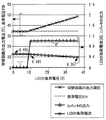
これに対して、LEDを定電力で駆動することが考えられる(例えば、特許文献1〜3参照)。図13はLEDを定電力制御した場合の温度変化時の特性を示す図である。定電力制御の場合、低温時は負荷電圧が上昇した分、負荷電流を減らして電力を一定とするため、バッテリの持続時間を増やせる。光出力は減少するが、元々LEDの温度特性で明るさが増加しているため、必要な明るさは確保でき、無駄な光出力の増加を抑えることができる。一方、高温時は負荷電圧が減少するため負荷電流が増加する。これによって光出力が増加するが、LEDの温度特性で明るさが減少しているため、これを補う動作となる。ただし、一般的にLEDの温度特性の方が大きいため、定電力制御では完全には補いきれない。 On the other hand, it is possible to drive LED by constant power (for example, refer patent documents 1-3). FIG. 13 is a diagram showing the characteristics at the time of temperature change when constant power control of the LED is performed. In the case of constant power control, since the load current is reduced and the power is made constant by the amount of increase in load voltage at low temperature, the duration of the battery can be increased. Although the light output decreases, the brightness is originally increased due to the temperature characteristics of the LED, so that the necessary brightness can be secured, and an increase in the useless light output can be suppressed. On the other hand, when the temperature is high, the load voltage decreases and the load current increases. Although this increases the light output, the brightness decreases due to the temperature characteristics of the LED, so this operation is compensated. However, since the temperature characteristic of the LED is generally larger, constant power control can not completely compensate.
定電力制御ではLEDのばらつき、温度特性、故障、あるいは断線などで負荷電流が変化した場合にそれに応じて負荷電圧が変化する。同様に負荷電圧が変化した場合にそれに応じて負荷電流が変化する。特に電流がゼロになる開放時、電圧がゼロになる短絡時にそれぞれ電圧、電流が最大になる。この時の最大値が部品の定格を超えない様に過電流及び過電圧から保護する必要がある。 In the constant power control, when the load current changes due to the variation of the LED, the temperature characteristic, the failure or the disconnection, the load voltage changes accordingly. Similarly, when the load voltage changes, the load current changes accordingly. In particular, at the time of open circuit when the current becomes zero, the voltage and current become maximum at the short circuit when the voltage becomes zero. It is necessary to protect against over current and over voltage so that the maximum value at this time does not exceed the rating of the component.
特開2009−231147号公報に記載の点灯装置は、電圧リミット及び電流リミットを行うための回路として、比較器およびダイオードオア回路を備えている。しかしながら、この公報に記載の回路では、正常なLED電圧検出信号に対して、電圧リミッタ検出信号または電流リミッタ検出信号がダイオードオア回路により割り込むという回路動作となる。ダイオードオア回路により3つの検出信号のうち最大値のみが制御回路へと入力されるので、電圧リミッタと電流リミッタのいずれか一方のみが動作し、これらが両方同時に動作することはできない。このような択一的なリミッタ動作は、定電力制御を行う観点からはいまだ改善の余地を残すものであった。 The lighting device described in JP2009-231147A includes a comparator and a diode-OR circuit as a circuit for performing voltage limit and current limit. However, the circuit described in this publication has a circuit operation in which the voltage limiter detection signal or the current limiter detection signal is interrupted by the diode OR circuit with respect to the normal LED voltage detection signal. Since only the maximum value among the three detection signals is input to the control circuit by the diode OR circuit, only one of the voltage limiter and the current limiter operates, and both of them can not operate simultaneously. Such alternative limiter operation still leaves room for improvement from the viewpoint of performing constant power control.
本発明は、上述のような課題を解決するためになされたもので、その目的は定電力制御を行うとともに過電流及び過電圧から保護することができるLED点灯装置を得るものである。 The present invention has been made to solve the problems as described above, and an object thereof is to obtain an LED lighting device capable of performing constant power control and protecting against over current and over voltage.
第1の発明にかかるLED点灯装置は、LEDのアノードに負荷電流を供給して前記LEDを点灯させる電源回路と、前記LEDのカソードとグランド端子の間に直列接続された第1抵抗と、一端および他端を有し、前記一端が前記LEDのカソードと前記第1抵抗の接続点に接続された第2抵抗と、一端および他端を有し、前記一端に前記LEDのアノード電圧に応じた電圧が印加される第3抵抗と、前記第2抵抗の前記他端と前記第3抵抗の前記他端とを接続した接続点の電圧、又は前記第2抵抗の前記他端の電圧と前記第3抵抗の前記他端の電圧とを乗算した電圧と、予め定めた所定値と、の差を前記電源回路にフィードバックするエラーアンプと、前記第2抵抗と並列に接続し、前記第2抵抗の前記一端に印加される電圧が予め定めた電圧を上回ると、前記電源回路の出力に上限を設けるように前記第2抵抗の前記他端の電圧を調整する第1リミッタ回路と、前記LEDの負荷電圧に上限を設ける第2リミッタ回路と、を備え、前記電源回路は、前記LEDの点灯中に前記差を減少させるように出力を制御する。 According to a first aspect of the present invention, there is provided an LED lighting device comprising: a power supply circuit for supplying a load current to an anode of an LED to light the LED; a first resistor serially connected between a cathode of the LED and a ground terminal; And a second resistor having one end and the other end connected to the connection point of the cathode of the LED and the first resistor, and one end and the other end according to the anode voltage of the LED at the one end A third resistor to which a voltage is applied, a voltage at a connection point connecting the other end of the second resistor and the other end of the third resistor, or a voltage of the other end of the second resistor and the An error amplifier for feeding back to the power supply circuit a difference between a voltage obtained by multiplying the voltage at the other end of the three resistors and a predetermined value determined in advance, and connected in parallel to the second resistor, the second resistor The voltage applied to the one end is predetermined A first limiter circuit that adjusts a voltage of the other end of the second resistor to set an upper limit to an output of the power supply circuit when the voltage is exceeded; and a second limiter circuit that sets an upper limit to a load voltage of the LED; And the power supply circuit controls the output to reduce the difference during lighting of the LED.
第2の発明にかかるLED点灯装置は、LEDのアノードに負荷電流を供給して前記LEDを点灯させる電源回路と、前記LEDのカソードとグランド端子の間に直列接続された第1抵抗と、一端および他端を有し、前記一端が前記LEDのカソードと前記第1抵抗の接続点に接続された第2抵抗と、一端および他端を有し、前記一端に前記LEDのアノード電圧に応じた電圧が印加される第3抵抗と、前記第2抵抗の前記他端と前記第3抵抗の前記他端とを接続した接続点の電圧又は前記第2抵抗の前記他端の電圧と前記第3抵抗の前記他端の電圧とを乗算した電圧と、予め定めた所定値と、の差を前記電源回路にフィードバックするエラーアンプと、前記第3抵抗の前記一端の電圧が基準電圧を下回らないように、前記第3抵抗の前記一端の電圧に下限を設ける第3リミッタ回路と、前記LEDの負荷電圧に上限を設ける第4リミッタ回路と、を備え、前記電源回路は、前記LEDの点灯中に前記差を減少させるように出力を制御する。 According to a second aspect of the present invention, there is provided an LED lighting device comprising: a power supply circuit for supplying a load current to an anode of an LED to light the LED; a first resistor serially connected between a cathode of the LED and a ground terminal; And a second resistor having one end and the other end connected to the connection point of the cathode of the LED and the first resistor, and one end and the other end according to the anode voltage of the LED at the one end A third resistor to which a voltage is applied, a voltage at a connection point connecting the other end of the second resistor and the other end of the third resistor, or a voltage of the other end of the second resistor and the third An error amplifier for feeding back a difference between a voltage obtained by multiplying the voltage at the other end of the resistor and a predetermined value determined in advance to the power supply circuit and a voltage at the one end of the third resistor do not fall below the reference voltage. And the one of the third resistors And a fourth limiter circuit for setting an upper limit on the load voltage of the LED, wherein the power supply circuit is configured to reduce an output while the LED is lit. Control.
第3の発明にかかるLED点灯装置は、LEDのアノードに負荷電流を供給して前記LEDを点灯させる電源回路と、前記負荷電流を検知する第一検知手段と、前記LEDに印加される負荷電圧を検知する第二検知手段と、前記第二検知手段で検知した値が予め定めた下限値を下回らないときには前記第二検知手段で検知した値を出力し、前記第二検知手段で検知した値が前記下限値を下回るときには前記下限値を出力する低電圧リミッタと、前記第一検知手段で検知した値と、前記低電圧リミッタが出力した値と、を加算または乗算した値を出力する演算手段と、前記演算手段の出力する値に上限を設ける高電圧リミッタと、前記高電圧リミッタの制限を受けた前記演算手段からの出力値と、予め定めた所定値と、の差を前記電源回路にフィードバックする比較手段と、を備え、前記電源回路は、前記LEDの点灯中に前記差を減少させるように出力を制御する。 According to a third aspect of the present invention, there is provided an LED lighting device comprising: a power supply circuit for supplying a load current to an anode of an LED to light the LED; first detection means for detecting the load current; and a load voltage applied to the LED And a value detected by the second detection means when the value detected by the second detection means does not fall below a predetermined lower limit. A computing means for outputting a value obtained by adding or multiplying a low voltage limiter for outputting the lower limit value when the value is lower than the lower limit value, a value detected by the first detection means and a value output from the low voltage limiter And a high voltage limiter for providing an upper limit to the value output from the calculation means, and a difference between an output value from the calculation means limited by the high voltage limiter and a predetermined value determined in advance to the power supply circuit. The A comparison means for feedback, the power supply circuit controlling the output to reduce the difference during lighting of the LED.
第1〜3の発明によれば、定電力制御を行うLED点灯装置において、リミッタの動作が反映された後の値が加算または乗算された算出値を、電源回路にフィードバックすることができる。これにより、電流リミッタと電圧リミッタの両方を同時に作動させることができ、リミッタされた許容範囲内で最大電力を設定可能な定電力制御を実現することができる。 According to the first to third invention, the LED lighting device that performs the constant power control, the calculated value of the value after the operation of the limiter is reflected is addition or multiplication can be fed back to the power supply circuit. Thereby, both the current limiter and the voltage limiter can be operated at the same time, and constant power control capable of setting the maximum power within the limited tolerance can be realized.
本発明の実施の形態に係るLED点灯装置について図面を参照して説明する。同じ又は対応する構成要素には同じ符号を付し、説明の繰り返しを省略する場合がある。 An LED lighting device according to an embodiment of the present invention will be described with reference to the drawings. The same or corresponding components may be assigned the same reference numerals and repetition of the description may be omitted.
実施の形態1.
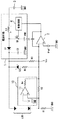
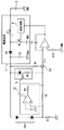
図1は、本発明の実施の形態1に係るLED点灯装置を示す図である。電源回路1はLEDのアノードに負荷電流を供給してLEDを点灯させる。抵抗R1がLEDのカソードとグランド端子(GND)の間に接続されている。
FIG. 1 is a diagram showing an LED lighting device according to
抵抗R2の一端がLEDのカソードと抵抗R1との接続点に接続されている。抵抗R3の一端がLEDのアノードに接続され、抵抗R3の他端が抵抗R2の他端に接続されている。 One end of the resistor R2 is connected to the connection point between the cathode of the LED and the resistor R1. One end of the resistor R3 is connected to the anode of the LED, and the other end of the resistor R3 is connected to the other end of the resistor R2.
エラーアンプ2は抵抗R2と抵抗R3の接続点の電圧Vinを電源回路1にフィードバックする。エラーアンプ2は差動増幅回路であり、負極入力から電圧Vinを入力し、正極入力から基準電圧Vrefを入力する。エラーアンプ2の負極入力と出力との間にコンデンサC1が接続されている。
The error amplifier 2 feeds back the voltage Vin at the connection point between the resistors R2 and R3 to the
電源回路1は、インダクタL1、MOSFETなどのスイッチング素子Q1、ダイオードD1、及び平滑コンデンサC2を有するチョッパ回路である。インダクタL1の一端がバッテリ3に接続されている。スイッチング素子Q1は、インダクタL1の他端とグランド端子(GND)の間に接続されている。ダイオードD1のアノードがインダクタL1の他端に接続され、ダイオードD1のアノードとインダクタL1の他端との接続点とスイッチング素子Q1のドレインが接続されている。平滑コンデンサC2の正極がダイオードD1のカソードに接続され、負極がグランド端子(GND)に接続されている。
The
スイッチング素子Q1は制御回路4により制御される。スイッチング素子Q1をオン/オフさせると、スイッチング素子Q1のオン期間にインダクタL1に蓄積されたエネルギーが、スイッチング素子Q1のオフ期間にダイオードD1を介して放出される。そして、バッテリ3の出力電圧にインダクタL1から放出されるエネルギーが重畳される形で平滑コンデンサC2が充電されるため、平滑コンデンサC2の両端電圧をバッテリ3の出力電圧よりも昇圧することができる。
The switching element Q1 is controlled by the
制御回路4は、エラーアンプ2の出力に応じてスイッチング素子Q1のオン/オフの周波数又はデューティ比を制御する。これにより、電源回路1は、抵抗R2と抵抗R3の接続点の電圧Vinが一定になるように出力を制御する。なお、制御回路4は、制御IC、又はCPU、システムLSI等の処理回路により実現される。また、複数の処理回路が連携して上記機能を実行してもよい。
The
実施の形態1に係るLED点灯装置は、電流リミッタ回路10を備えている。電流リミッタ回路10は、抵抗R2に並列に接続している。具体的には、コンパレータ11の正極入力が抵抗R2と抵抗R1との接続点に接続されている。コンパレータ11の負極入力には予め定めた電圧が印加されている。コンパレータ11の出力は抵抗R4の一端に接続し、抵抗R4の他端は、抵抗R2の他端と抵抗R3の他端とが接続する接続点に接続している。
The LED lighting device according to the first embodiment includes the
ツェナーダイオードDZ2および抵抗R5の直列回路が、R3に並列に接続されている。このツェナーダイオードDZ2および抵抗R5の直列回路は、本発明にかかる「電圧リミッタ回路」に相当している。 A series circuit of a Zener diode DZ2 and a resistor R5 is connected in parallel to R3. The series circuit of the Zener diode DZ2 and the resistor R5 corresponds to the "voltage limiter circuit" according to the present invention.
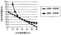
LEDの負荷電流は抵抗R1に印加される電圧に対応し、LEDの負荷電圧は抵抗R3に印加される電圧に対応する。このため、抵抗R2と抵抗R3の接続点の電圧VinはLEDの負荷電流と負荷電圧の加算に対応する。従って、エラーアンプ2はLEDの負荷電流と負荷電圧の加算を電源回路1にフィードバックする。一方、電力は負荷電流と負荷電圧の乗算である。図2はLEDの負荷電流と負荷電圧の加算と乗算の関係を示す図である。図2に示すように、加算を一定にする制御(加算一定制御)と乗算を一定にする制御(乗算一定制御)は異なる。
The load current of the LED corresponds to the voltage applied to the resistor R1, and the load voltage of the LED corresponds to the voltage applied to the resistor R3. Therefore, the voltage Vin at the connection point between the resistor R2 and the resistor R3 corresponds to the addition of the load current and the load voltage of the LED. Therefore, the
しかし、LEDを負荷とした場合、負荷電圧の変化範囲は数V程度と小さい。図3は、図2における負荷電圧の使用範囲を拡大した図である。図3に示すように、負荷電圧の使用範囲内では乗算一定制御を加算一定制御によって近似することができる。また、負荷電圧の使用範囲外では乗算一定制御のカーブから加算一定制御が外れるが、加算一定制御の方が電力が低くなる方向に外れるため、安全である。 However, when an LED is used as a load, the change range of the load voltage is as small as several volts. FIG. 3 is an enlarged view of a use range of the load voltage in FIG. As shown in FIG. 3, constant multiplication control can be approximated by constant addition control within the use range of the load voltage. Further, although the addition constant control deviates from the curve of the multiplication constant control outside the use range of the load voltage, the addition constant control deviates in the direction in which the power becomes lower, which is safe.
電流リミッタ回路10は、抵抗R2の一端に印加される電圧が予め定めた電圧を上回ると抵抗R2の他端に電圧を加算することで、過電流保護を実現する。具体的には、コンパレータ11は、抵抗R2の一端に印加される電圧(すなわち抵抗R1とLEDのカソードの接続点の電圧)が予め定めた電圧を上回ったときにハイとなる。コンパレータ11がハイとなることで、コンパレータ11の出力電圧が抵抗R2の他端に加算される。その結果、電圧Vinを増大させて電源回路1の出力を低下させようとする回路動作が得られる。すなわち、エラーアンプ2により加算値(または後述するように乗算値)としての電圧Vinが電源回路1にフィードバックされることで、定電力制御が実現される。この電圧Vinを一定に保つために、電圧Vinが増加したときにはその増加分を減らすように電源回路1が出力を低下させる。過電流発生時には、電流リミッタ回路10が電圧Vinを上げるように働くので、電流リミッタ回路10による電圧加算分だけ電圧Vinがより大きな値として算出される。よって、過電流発生時には、増加補正した電圧Vinによって、電源回路1の出力を下げる方向にフィードバックをかけることができる。その結果、電流リミッタ回路10の電圧加算により負荷電流に上限を設けることができる。好ましくは、電流リミッタ回路10は、負荷電圧がある値以下となっている場合には、負荷電圧にかかわらず負荷電流がある上限値で固定されるように、負荷電流の上限を設けることが好ましい。具体的には、電流リミッタ回路10の電圧加算によって電圧Vinが増加補正され、図3に示すごとく、負荷電圧にかかわらず負荷電流をある上限で止めるように電源回路1の出力を制限することが好ましい。
The
過電圧からの保護を行うために、LEDの負荷電圧が一定値を超えた場合にツェナーダイオードDZ2がオンする。ツェナーダイオードDZ2の動作点は使用範囲の外に設け、電力を低下させる方向に変化させることで故障を避け安全な動作となるように設定する。特開2009−231147号公報の図に記載されるようにコンパレータを用いて電圧リミッタ回路を組む必要が無いので、簡素な構成で電圧のリミッタ回路を構成することができる。 The zener diode DZ2 is turned on when the load voltage of the LED exceeds a certain value in order to protect against an overvoltage. The operating point of the Zener diode DZ2 is provided outside the usable range, and the power is changed in the direction to reduce the power, thereby setting the operation to avoid a failure and to be a safe operation. As described in JP 2009-231147 A, since it is not necessary to form a voltage limiter circuit using a comparator, the voltage limiter circuit can be configured with a simple configuration.
以上説明したように、本実施の形態ではLEDの負荷電流と負荷電圧を加算した値を電源回路1にフィードバックすることで、簡単な回路構成によりLEDを定電力制御できる。
As described above, in the present embodiment, constant power control of the LED can be performed with a simple circuit configuration by feeding back the value obtained by adding the load current of the LED and the load voltage to the
また、エラーアンプ2に入力される電圧Vinは以下の数式1で求められる。
![]()
![]()
これらのパラメータにおいて下記の数式2で抵抗R2,R3の抵抗値r2,r3を決定すれば、この負荷電圧VF付近ではP´=0となり、電力Pが一定となる。従って、電力Pおよび抵抗R1の抵抗値r1に関わらず定電力制御を行うことができる。また、定数設計が簡単にできる。
![]()
![]()
また、負荷電圧を求めるための抵抗R3に並列にツェナーダイオードDZ2を接続し、負荷電圧が一定値を超えた場合にツェナーダイオードDZ2をオンさせる。これにより、LED、抵抗R1、電源回路1内の素子を過電圧から保護することができる。
Further, a Zener diode DZ2 is connected in parallel with a resistor R3 for obtaining a load voltage, and the Zener diode DZ2 is turned on when the load voltage exceeds a predetermined value. Thus, the LED, the resistor R1, and the elements in the
実施の形態2.
図4は、本発明の実施の形態2に係るLED点灯装置を示す図である。実施の形態2にかかるLED点灯装置は、電流リミッタ回路10をツェナーダイオードDZ1に置換している点、および図1ではツェナーダイオードDZ2に抵抗R5を直列接続しているが図4ではこれを省略する変形を行っておりツェナーダイオードDZ2単体で電圧リミッタ回路を構成している点を除き、図1に示す実施の形態1にかかるLED点灯装置と同様の回路構成を備えている。したがって、以下の説明では実施の形態1と同一または相当する構成については同一の符号を付して説明を行うとともに、実施の形態1との相違点を中心に説明し、共通事項は説明を簡略化ないしは省略する。
Second Embodiment
FIG. 4 is a diagram showing an LED lighting device according to
実施の形態2では、ツェナーダイオードDZ1が抵抗R2に並列に接続されている。過電流から保護するために、負荷電流が一定値を超えた場合にツェナーダイオードDZ1をオンさせる。ツェナーダイオードDZ1の動作点は使用範囲の外に設け、電力を低下させる方向に変化させることで故障を避け安全な動作となるように設定する。ツェナーダイオードDZ1がオンとなれば抵抗R2の両端の電圧が一定に保持されるので、抵抗R2の他端の電圧を一定値に制限でき、電圧Vinを制限することができる。電圧Vinを制限することで、電源回路1の出力が制限されるので、過電流発生時に電源回路1が出力を増加させないように上限を設けることができる。
In the second embodiment, the Zener diode DZ1 is connected in parallel to the resistor R2. In order to protect against an overcurrent, the Zener diode DZ1 is turned on when the load current exceeds a certain value. The operating point of the Zener diode DZ1 is provided outside the use range, and by changing the power in the direction of reduction, the failure is avoided and the safe operation is set. When the Zener diode DZ1 is turned on, the voltage across the resistor R2 is kept constant, so the voltage at the other end of the resistor R2 can be limited to a constant value, and the voltage Vin can be limited. Since the output of the
以上説明したように、実施の形態2では、負荷電流と負荷電圧を求めるための抵抗R2,R3にそれぞれ並列にツェナーダイオードDZ1,DZ2を接続し、負荷電流及び負荷電圧がそれぞれ一定値を超えた場合にツェナーダイオードDZ1,DZ2をオンさせる。これにより、簡単な回路構成で、LED、抵抗R1、電源回路1内の素子を過電流及び過電圧から保護することができる。また、特開2009−231147号公報の図に記載されるようにコンパレータを3つ並列に接続するような複雑な回路を組む必要が無いので、簡素な構成で電流および電圧のリミッタ回路を構成することができる。
As described above, in the second embodiment, the Zener diodes DZ1 and DZ2 are connected in parallel to the resistors R2 and R3 for obtaining the load current and the load voltage, respectively, and the load current and the load voltage each exceed a predetermined value. In this case, the Zener diodes DZ1 and DZ2 are turned on. This makes it possible to protect the LED, the resistor R1, and the elements in the
実施の形態3.
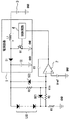
図5は、本発明の実施の形態3に係るLED点灯装置を示す図である。本実施の形態では、図4に示す実施の形態2のツェナーダイオードDZ1,DZ2の代わりに高電圧リミッタ回路5と低電圧リミッタ回路6が設けられている。また、抵抗R2と抵抗R3の接続点とエラーアンプ2の間に抵抗R4が接続されている。その他の構成は実施の形態2と同様である。
Third Embodiment
FIG. 5 is a diagram showing an LED lighting device according to
高電圧リミッタ回路5は抵抗R2と抵抗R3の接続点とLEDのアノードの間に接続されている。高電圧リミッタ回路5は直列に接続されたツェナーダイオードDZ3と抵抗R5を有する。低電圧リミッタ回路6は抵抗R3の一端に接続され、低電圧リミッタ回路6はコンパレータ7と切替回路8を有する。コンパレータ7はLEDのアノード電圧と基準電圧Vthを比較する。切替回路8は、アノード電圧が基準電圧Vth以上の場合には抵抗R3の一端にアノード電圧を印加し、アノード電圧が基準電圧Vthを下回る場合には抵抗R3の一端に基準電圧Vthを印加するように接続を切り替える。これにより、低電圧リミッタ回路6は抵抗R3の一端の電圧が基準電圧Vthを下回らないように制限する。
The high
また、過電圧から保護するために、負荷電圧が一定値を超えた場合に高電圧リミッタ回路5のツェナーダイオードDZ3をオンさせ、LEDの負荷電圧の上限を設定する。ツェナーダイオードDZ3の動作点は使用範囲の外に設け、電力を低下させる方向に変化させることで故障を避け安全な動作となるように設定する。
Also, in order to protect from an overvoltage, when the load voltage exceeds a certain value, the Zener diode DZ3 of the high
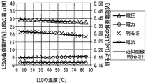
また、低電圧リミッタ回路6は抵抗R3の一端の電圧が基準電圧Vthを下回らないように制限する。図6は、本発明の実施の形態3に係る低電圧リミッタ回路の動作を説明するための図である。ここで、抵抗R1の抵抗値を1Ω、抵抗R2の抵抗値を4.0367KΩ、抵抗R3の抵抗値を440KΩ、基準電圧Vthを34V、基準電圧Vrefを0.8V、定電力値を17.7Wとした。 In addition, the low voltage limiter circuit 6 limits the voltage at one end of the resistor R3 so as not to fall below the reference voltage Vth. FIG. 6 is a diagram for explaining the operation of the low voltage limiter circuit according to the third embodiment of the present invention. Here, the resistance value of the resistor R1 is 1Ω, the resistance value of the resistor R2 is 4.0367 KΩ, the resistance value of the resistor R3 is 440 KΩ, the reference voltage Vth is 34 V, the reference voltage Vref is 0.8 V, and the constant power value is 17.7 W And
LEDの負荷電圧が48Vから30Vまで低下する場合において、基準電圧Vth=34Vまではコンパレータ7は”H”を出力する。これに応じて切替回路8は抵抗R3の一端にLEDのアノード電圧を印加する。
When the load voltage of the LED decreases from 48 V to 30 V, the
その後、LEDの負荷電圧が基準電圧Vth=34Vを下回ると、コンパレータ7は”L”を出力し、切替回路8は抵抗R3の一端に基準電圧Vthを印加する。この結果、LEDの負荷電圧が34Vを下回っても、抵抗R3の一端に34Vが入力される。
Thereafter, when the load voltage of the LED falls below the reference voltage Vth = 34 V, the
LEDの負荷電流が増加していくと負荷電圧が低下していくため、定電力制御だけでは過電流を防げない。そこで、抵抗R3の一端の電圧が基準電圧よりも低下しないように低電圧リミッタ回路6が制限することで、LEDの負荷電流は一定値(0.495A)より大きくならない。この結果、過電流から保護することができる。 Since the load voltage decreases as the LED load current increases, the constant power control alone can not prevent the overcurrent. Therefore, the load current of the LED does not exceed the fixed value (0.495 A) by limiting the low voltage limiter circuit 6 so that the voltage at one end of the resistor R3 does not fall below the reference voltage. As a result, it is possible to protect against overcurrent.
以上説明したように、本実施の形態ではLEDの負荷電流と負荷電圧を加算した値を電源回路1にフィードバックすることで簡単な回路構成によりLEDを定電力制御できる。
As described above, in the present embodiment, constant power control of the LED can be performed with a simple circuit configuration by feeding back the value obtained by adding the load current of the LED and the load voltage to the
また、高電圧リミッタ回路5がLEDの負荷電圧の上限を設定することで過電圧から保護することができる。さらに、低電圧リミッタ回路6により抵抗R3の一端の電圧が基準電圧Vthを下回らないように制限する。これにより過電流から保護することができる。
Further, the high
実施の形態4.
図7は、本発明の実施の形態4に係るLED点灯装置を示す図である。図5に示す実施の形態3の低電圧リミッタ回路6の代わりに低電圧リミッタ回路9を設けている。その他の構成は実施の形態3と同様である。
Fourth Embodiment
FIG. 7 is a diagram showing an LED lighting device according to
低電圧リミッタ回路9は抵抗R6,R7,R8、MOSFETなどのトランジスタQ2、シャントレギュレータ21、およびバイアス抵抗R21を有する。抵抗R6はLEDのアノードと抵抗R3の一端の間に接続されている。トランジスタQ2のエミッタが抵抗R3と抵抗R6の接続点に接続され、コレクタがLEDのアノードに接続されている。バイアス抵抗R21の一端はトランジスタQ2のコレクタと接続し、バイアス抵抗R21の他端はトランジスタQ2のベースとシャントレギュレータ21のカソードとの接続点に接続している。シャントレギュレータ21は、抵抗R3と抵抗R6の接続点の電圧を抵抗R7、R8で分圧したものをリファレンス電圧として入力し、バイアス抵抗R21から供給される電流により、トランジスタQ2のベースに出力電圧を印加する。
The low
図8は、本発明の実施の形態4に係る低電圧リミッタ回路の動作を説明するための図である。ここで、抵抗R1の抵抗値を1Ω、抵抗R2の抵抗値を4.0367KΩ、抵抗R3の抵抗値を22KΩ、抵抗R6の抵抗値を418KΩ、シャントレギュレータ21の基準電圧を3.06V、リファレンス電圧Vrefを0.8V、定電力値を17.8Wとした。
FIG. 8 is a diagram for explaining the operation of the low voltage limiter circuit according to the fourth embodiment of the present invention. Here, the resistance value of the resistor R1 is 1Ω, the resistance value of the resistor R2 is 4.0367 KΩ, the resistance value of the resistor R3 is 22 KΩ, the resistance value of the resistor R6 is 418 KΩ, the reference voltage of the
LEDの負荷電圧が48Vから低下する場合、抵抗R3と抵抗R6の接続点の電圧も低下するが、シャントレギュレータ21の出力電圧よりも高い場合はそのままエラーアンプ2に送られる。この時、シャントレギュレータ21は、リファレンス電圧が閾値より高いため、出力電圧を下げる方向に動作する。従って、トランジスタQ2のベース電圧が低下し、ベース・エミッタが逆方向にバイアスされるため、シャントレギュレータ21の出力電圧はトランジスタQ2のエミッタには発生しない。例えばトランジスタQ2のベース電圧は1V程度、エミッタ電圧2〜3Vである。
When the load voltage of the LED drops from 48 V, the voltage at the connection point of the resistors R3 and R6 also drops, but when it is higher than the output voltage of the
その後、LEDの負荷電圧が30V程度まで低下し、抵抗R3と抵抗R6の接続点の電圧がシャントレギュレータ21の出力電圧を下回ると、トランジスタQ2のベース・エミッタ間が導通し、抵抗R3と抵抗R6の接続点にはシャントレギュレータ21の出力電圧が発生する。従って、LEDの負荷電圧が基準電圧を下回っても、低電圧リミッタ回路9は抵抗R3の一端にシャントレギュレータ21の出力電圧が入力される。この結果、低電圧リミッタ回路9は抵抗R3の一端の電圧が基準電圧を下回らないように制限する。これにより実施の形態1〜3と同様の効果を得ることができる。
Thereafter, when the load voltage of the LED drops to about 30 V and the voltage at the connection point between the resistors R3 and R6 falls below the output voltage of the
また、実施の形態4では、実施の形態3の切替回路8をトランジスタQ2のベース・エミッタ間ダイオードによるダイオードオアで代用し、実施の形態3のコンパレータ7と基準電圧源をシャントレギュレータ21で代用している。従って、コンパレータを使用しないため、コンパレータそのものと電源回路を省略することができる。また、電源回路が無いため、電源電圧の増減による制約が無い。そして、トランジスタQ2が電圧を受け持つため、基準電圧を低く設定することができ、低圧なシャントレギュレータを使用することができる。さらに、出力用バッファと切替回路をトランジスタQ2で兼用するため、回路が簡略化される。
Further, in the fourth embodiment, the switching
実施の形態5.
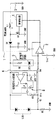
図9は、本発明の実施の形態5に係るLED点灯装置を示す図である。図5に示す実施の形態3の低電圧リミッタ回路6の代わりに低電圧リミッタ回路22を設けている。その他の構成は実施の形態3と同様である。
FIG. 9 is a diagram showing an LED lighting device according to
低電圧リミッタ回路22は抵抗R6,R9,ダイオードD5、およびツェナーダイオードDZ4を有する。抵抗R6はLEDのアノードと抵抗R3の一端の間に直列に接続されている。ダイオードD5のカソードが抵抗R3と抵抗R6の接続点に接続され、ダイオードD5のアノードがツェナーダイオードDZ4のカソードに接続されている。ツェナーダイオードDZ4のアノードはグランド端子に接続している。
The low
ここで実施の形態5の回路設計方法の一例を説明すると、降伏電圧が5.1VであるツェナーダイオードDZ4を選定して、抵抗R9とツェナーダイオードDZ4のカソードの接続点が5.1Vで維持されるように構成しておく。抵抗R3と抵抗R6の接続点の電圧が例えば通常7V程度となるように抵抗R3,R6を選定しておく。ダイオードD5のアノードに5.1Vが印加され、ダイオードD5のカソードに7V程度の電圧が印加されているときには、ダイオードD5に逆バイアスがかかっている。その後、LEDの負荷電圧が低下し、例えば抵抗R3と抵抗R6の接続点の電圧が7Vから4.5Vを下回るまで下がったとする。この場合、ダイオードD5のアノードの電圧5.1Vから0.6Vの電圧降下分を差し引いた4.5Vが抵抗R3と抵抗R6の接続点に供給され続けるので、抵抗R3の一端に印加される電圧に下限を設けることができる。これにより、低電圧リミッタ回路9は抵抗R3の一端の電圧が基準電圧を下回らないように制限する。これにより実施の形態1〜4と同様の効果を得ることができる。
To describe an example of a circuit design method of the fifth embodiment, where, by selecting the
また、実施の形態3などと比較して、トランジスタあるいはシャントレギュレータなどの回路部品を含まないので、回路構成が簡素化されているという利点もある。 Further, as compared with the third embodiment and the like, there is also an advantage that the circuit configuration is simplified since circuit components such as transistors or shunt regulators are not included.
実施の形態6.
図10は、本発明の実施の形態6にかかるLED点灯装置を示す図であり、マイコン34を用いたLED点灯装置を示す図である。この実施の形態6は、実施の形態1〜5に係る回路を集積化したLED点灯装置を提供するものである。マイコン34は、実施の形態1〜5における、抵抗R1〜R3による電圧検知機能、エラーアンプ2の機能、制御回路4の機能、低電圧リミッタ回路6、9、22の機能、高電圧リミッタ回路5の機能を内部に取り込んだものであり、これらの機能をそれぞれ実行するプログラムを内部のメモリに予め記憶している。なお、実施の形態6の電源回路101は、実施の形態1〜5における昇圧チョッパ回路部分(電源回路1のうちインダクタL1、スイッチング素子Q1、ダイオードD1、およびコンデンサC2で構成される部分)であり、マイコン34の外側に設けられている。電源回路1に含まれていた制御回路4はマイコン34側に搭載されている。抵抗R1、R3は、マイコン34の外側に設けられている。
Sixth Embodiment
FIG. 10 is a diagram showing an LED lighting device according to a sixth embodiment of the present invention, and a diagram showing an LED lighting device using the
マイコン34は、メモリおよびメモリに記憶されたプログラムを実行するCPUを備える形態、あるいはシステムLSI等の処理回路の形態で実現される。また、メモリ、CPU、および処理回路の少なくとも1種が複数個組み合わされてマイコン34を構成していても良く、複数の処理回路などが連携して上記機能を実行してもよい。マイコン34は、公知のデジタル制御電源用マイコンが備えるのと同様の構成を含んでおり、入出力インターフェース、A/D変換器、デジタル演算を行うためのプロセッサ、各種の揮発性・不揮発性メモリ、オシレータ、スイッチング素子のオンオフ制御に用いるPWM信号を生成するためのパルス幅モジュレータ、および各種周辺回路を含む。
The
図14は、実施の形態6に係るLED点灯装置が有するマイコン34の機能ブロック図である。一例として、マイコン34は、A/D変換部、高電圧リミッタ機能部、低電圧リミッタ機能部、フィードバック機能部(以下、FB機能部)、PWM信号生成機能部を備えている。FB機能部は、演算機能部および比較機能部を備えている。これらの機能部ごとの処理がモジュール化されたプログラムを内蔵不揮発性メモリに記憶しておき、プロセッサで実行することにより、マイコン34の機能を実現してもよい。以下、説明の便宜上、各機能ごとに機能部を分けつつマイコン34の処理内容について一例を説明する。
FIG. 14 is a functional block diagram of the
(処理S1)まずマイコン34は、抵抗R1の一端からの電圧をインターフェースを介して取得することでLEDの負荷電流に応じた電圧Vin1を取得する。また、マイコン34は、抵抗R3およびR102の分圧回路で分圧された電圧をインターフェースを介して取得することで、LEDの負荷電圧に応じた電圧Vin2を取得する。
(Process S1) First, the
(処理S2)次に、電圧Vin1、Vin2は、マイコン34内部においてA/D変換部によってデジタル値Vin1´、Vin2´に変換される。
(Process S2) Next, the voltages Vin1 and Vin2 are converted into digital values Vin1 ′ and Vin2 ′ by the A / D conversion unit in the
(処理S3)次に、LED負荷電流に応じた電圧Vin1をA/D変換したデジタル値Vin1´がマイコン34の低電圧リミッタ機能部に入力される。低電圧リミッタ機能部の動作は、実施の形態3〜5で述べた低電圧リミッタ回路6、9、22の入出力動作と同様である。つまり、低電圧リミッタ機能部は、Vin1´と下限値とを比較し、Vin1´が下限値以上であるときにはVin1´そのものを出力し、Vin1´が下限値を下回るときには下限値そのものを出力する。
(Processing S3) Next, a digital value Vin1 'obtained by A / D converting the voltage Vin1 corresponding to the LED load current is input to the low voltage limiter function unit of the
(処理S4)また、LED負荷電圧に応じた電圧Vin2をA/D変換したデジタル値Vin2´が高電圧リミッタ機能部に入力される。高電圧リミッタ機能部は、実施の形態1〜5で述べた高電圧リミッタ回路5、9、22の入出力動作と同様である。高電圧リミッタ機能部は、デジタル値Vin2´と予め定めた降伏電圧値VDZ´と比較する。降伏電圧値VDZ´は、上記実施の形態1および2にかかるツェナーダイオードDZ2および実施の形態3〜5で用いた高電圧リミッタ回路5における降伏電圧と同様の観点から設定された値である。
(Processing S4) Further, a digital value Vin2 'obtained by A / D converting the voltage Vin2 corresponding to the LED load voltage is input to the high voltage limiter function unit. The high voltage limiter function unit is the same as the input / output operation of the high
高圧リミッタ機能部は、上記実施の形態1および2にかかるツェナーダイオードDZ2および実施の形態3〜5で用いた高電圧リミッタ回路5と同様の機能を果たす。この点について実施の形態1〜5の回路動作を先ず説明すると、例えば図7に示す高電圧リミッタ回路5が有するツェナーダイオードDZ3の降伏電圧と同じ役割を降伏電圧値VDZ´が果たしている。LED電圧が上がりツェナーダイオードDZ3が導通すると、LED電圧の検出に用いられる抵抗R6,R3に対して、高電圧リミッタ回路5を構成する抵抗R5およびツェナーダイオードDZ3が並列に接続される。並列接続の結果、この経路のインピーダンスがツェナーダイオードDZ3の非導通時よりも下がる。インピーダンスが下がることで、同じLED電圧でも、抵抗R6,R3、R5およびツェナーダイオードDZ3で構成される並列回路の電流が増加するので、エラーアンプ2の負極入力電圧が上がる。その結果、その負極入力電圧の増加分を減らすように帰還がかかり、電源回路1は出力を低下させる。このように、実施の形態1〜5では、回路全体の動作として高電圧リミッタがかかるようになっている。
The high voltage limiter function unit performs the same function as the Zener diode DZ2 according to the first and second embodiments and the high
実施の形態6にかかる高電圧リミッタ機能部もこれと同様の機能を発揮するために、Vin2´とVDZ´とを比較し、その比較結果に応じて下記のいずれかの動作をする。まず、Vin2´がVDZ´よりも低いときには(Vin2´<VDZ´)、入力されたVin2´がそのままVhiとして出力される。LEDが正常であればLED電圧はVDZ´よりも低くなるようにVDZ´が設定される。従って、LEDが正常の特性を示している間は、高電圧リミッタ機能部はVin2´をそのまま出力する。一方、Vin2´がVDZ´以上となったときには(Vin´≧VDZ´)、入力されたVin2´よりも大きな値を出力値Vhiとして出力する。この時に高電圧リミッタ機能部が出力する値は予め記憶された所定値であってもよく、今回のVin2´に係数をかけて演算されてもよい。いずれにしろ、出力値VhiがVin2´よりも大きく算出されることで、「例えば図7のツェナーダイオードDZ3が導通したことでインピーダンスが下がり、同じLED電圧でも、抵抗R6,R3、R5およびツェナーダイオードDZ3で構成される並列回路の電流が増加し、エラーアンプ2の負極入力電圧が上がる」という回路動作に近似した制御を行うことができる。出力値Vhiが大きめに算出されることで、後述するフィードバック機能部で電源回路101の出力を下げようとする処理が行われるからである。
In order to exhibit the same function as that of the high voltage limiter function unit according to the sixth embodiment, Vin2 'and VDZ' are compared, and either of the following operations are performed according to the comparison result. First, when Vin2 'is lower than VDZ' (Vin2 '<VDZ'), the input Vin2 'is output as Vhi as it is. If the LED is normal, VDZ 'is set so that the LED voltage is lower than VDZ'. Therefore, while the LED indicates normal characteristics, the high voltage limiter function unit outputs Vin2 'as it is. On the other hand, when Vin2 'becomes equal to or greater than VDZ' (Vin'ZVDZ '), a value larger than the input Vin2' is output as the output value Vhi. At this time, the value output by the high voltage limiter functional unit may be a predetermined value stored in advance, or may be calculated by multiplying the current Vin2 ′ by a coefficient. In any case, when the output value Vhi is calculated to be larger than Vin2 ', "For example, the impedance is lowered by the conduction of the Zener diode DZ3 in FIG. 7, and even with the same LED voltage, the resistors R6, R3, R5 and the Zener diode It is possible to perform control similar to the circuit operation in which the current of the parallel circuit configured by DZ3 increases and the negative electrode input voltage of the
(処理S5)次に、低電圧リミッタ機能部の出力値Vloと、高電圧リミッタ機能部の出力値Vhiとが、フィードバック機能部における演算機能部に入力される。演算機能部は、VloとVhiとの加算値としての算出値Vinc´を出力する。なお、加算ではなく積算(乗算)した値を算出値Vinc´としてもよい。 (Process S5) Next, the output value Vlo of the low voltage limiter function unit and the output value Vhi of the high voltage limiter function unit are input to the arithmetic function unit in the feedback function unit. The arithmetic function unit outputs a calculated value Vinc ′ as an added value of Vlo and Vhi. A value obtained by integration (multiplication) instead of addition may be used as the calculated value Vinc '.
(処理S6)次に、この算出値Vinc´と、予め定められた参照電圧デジタル値Vref´とが比較機能部で比較され、その差分ΔVin´が算出される。この差分ΔVin´がフィードバック機能部の出力となり、PWM信号生成機能部に入力される。 (Processing S6) Next, the calculated value Vinc 'and the predetermined reference voltage digital value Vref' are compared by the comparison function unit, and the difference ΔVin 'is calculated. The difference ΔVin 'is an output of the feedback function unit and is input to the PWM signal generation function unit.
(処理S7)差分ΔVin´がプラスであれば、PWM信号生成機能部は、LEDに供給する電力を下げるためにスイッチング素子Q1に与えるべきオン/オフ信号の周波数又はデューティ比を減らす。逆にその差分ΔVin´がマイナスであれば、PWM信号生成機能部は、LEDに供給する電力を上げるためにスイッチング素子Q1に与えるべきオン/オフ信号の周波数又はデューティ比を上げる。差分ΔVin´に基づいてフィードバック的に調整されたPWM信号Voutが、インターフェースを介してスイッチング素子Q1の制御端子に供給される。 (Process S7) If the difference ΔVin ′ is positive, the PWM signal generation function unit reduces the frequency or duty ratio of the on / off signal to be supplied to the switching element Q1 to reduce the power supplied to the LED. Conversely, if the difference ΔVin ′ is negative, the PWM signal generation function unit raises the frequency or duty ratio of the on / off signal to be supplied to the switching element Q1 to increase the power supplied to the LED. The PWM signal Vout adjusted in a feedback manner based on the difference ΔVin ′ is supplied to the control terminal of the switching element Q1 through the interface.
以上の処理により過電流および過電圧に対する保護を行いつつ定電流制御が可能なマイコン34が提供される。
Thus, the
変形例.
実施の形態1では抵抗R1、R2、およびR3を接続することで負荷電圧と負荷電流を加算した電圧Vinを生成し、この電圧Vinをエラーアンプ2で電源回路1にフィードバックしている。これにより、簡単な回路構成によりLEDを定電力制御できる。しかしながら、本発明はこれに限られず、図11のように負荷電圧と負荷電流の乗算器30(具体的には専用ICかマイコン)を用いても良い。図11は、本発明の実施の形態において乗算器を用いる場合の一例として実施の形態1に係るLED点灯装置を変形した図である。抵抗R2の他端と抵抗R3の他端と接続する乗算器30を設けている点を除き、図1と同様の回路である。乗算器30の出力は、エラーアンプ2に入力される。なお、実施の形態2〜5においても同様に乗算器30を設けてもよい。
Modified example.
In the first embodiment, by connecting the resistors R1, R2 and R3, a load voltage and a load current are added to generate a voltage Vin, which is fed back to the
なお、上述した実施の形態1、2にかかるLED点灯装置が、前記第1の発明にかかるLED点灯装置の具体的な実施形態に相当しており、上述した実施の形態3〜5にかかるLED点灯装置が、前記第2の発明にかかるLED点灯装置の具体的な実施形態に相当している。上述した実施の形態6にかかる点灯装置が、前記第3の発明にかかるLED点灯装置の具体的な実施形態に相当している。 The LED lighting device according to the first and second embodiments described above corresponds to a specific embodiment of the LED lighting device according to the first invention, and the LED according to the third to fifth embodiments described above. The lighting device corresponds to a specific embodiment of the LED lighting device according to the second invention. The lighting device according to the sixth embodiment described above corresponds to a specific embodiment of the LED lighting device according to the third aspect of the present invention.
実施の形態1、2にかかるLED点灯装置によれば、過電流時に電流リミッタ回路10が電圧を調整することにより定電力制御に用いる電圧Vinを補正することができ過電流保護を確実に行うとともに、ツェナーダイオードDZ2(電圧リミッタ回路)で過電圧から回路を確実に保護することができる。定電力制御では、出力電力を一定に保つように電源回路1がその出力を変化させる。過電流発生時に第1リミッタ回路が電圧を調整することで、電源回路1の出力を制限することができる。これにより、定電力制御において、過電流の発生時に負荷電流の上限を設けるように電源回路1の出力を制限する動作を実現できる。
According to the LED lighting device according to the first and second embodiments, the voltage Vin used for constant power control can be corrected by adjusting the voltage by the
実施の形態3〜5にかかるLED点灯装置によれば、過電流時に低電圧リミッタ回路6、9、22が電圧を制限することにより定電力制御に用いる電圧値Vinの減少を抑制することができ過電流を確実に保護するとともに、高電圧リミッタ回路5で過電圧から回路を確実に保護することができる。過電流の発生が推測されるアノード電圧低下時に、低電圧リミッタ回路6、9、22が第3抵抗R3一端の電圧低下に制限を設ける。第3抵抗R3の一端の電圧に下限が設けられることで、過電流発生時の電圧Vinが小さくなりすぎることが防止される。よって、過電流発生時にもかかわらず電源回路1の出力を増加させるようなフィードバック制御が行われることを抑制することができる。これにより、定電力制御において、過電流の発生時に負荷電流の上限を設けるように電源回路1の出力を制限する動作を実現できる。
According to the LED lighting device according to the third to fifth embodiments, when the low
1 電源回路、2 エラーアンプ、3 バッテリ、4 制御回路、5 高電圧リミッタ回路、6、9、22 低電圧リミッタ回路、7 コンパレータ、8 切替回路、10 電流リミッタ回路、21 シャントレギュレータ、11 コンパレータ、30 乗算器、34 マイコン、C1 コンデンサ、C2 平滑コンデンサ、D1 ダイオード、D5 ダイオード、DZ1,DZ2、DZ3、DZ4 ツェナーダイオード、L1 インダクタ、Q1 スイッチング素子、Q2 トランジスタ、R21 バイアス抵抗 1 power supply circuit, 2 error amplifier, 3 batteries, 4 control circuits, 5 high voltage limiter circuits, 6, 9, 22 low voltage limiter circuits, 7 comparators, 8 switching circuits, 10 current limiter circuits, 21 shunt regulators, 11 comparators, 30 multiplier, 34 microcomputer, C1 capacitor, C2 smoothing capacitor, D1 diode, D5 diode, DZ1, DZ2, DZ3, DZ4 Zener diode, L1 inductor, Q1 switching element, Q2 transistor, R21 bias resistor
Claims (11)
前記LEDのカソードとグランド端子の間に直列接続された第1抵抗と、
一端および他端を有し、前記一端が前記LEDのカソードと前記第1抵抗の接続点に接続された第2抵抗と、
一端および他端を有し、前記一端に前記LEDのアノード電圧に応じた電圧が印加される第3抵抗と、
前記第2抵抗の前記他端と前記第3抵抗の前記他端とを接続した接続点の電圧、又は前記第2抵抗の前記他端の電圧と前記第3抵抗の前記他端の電圧とを乗算した電圧と、予め定めた所定値と、の差を前記電源回路にフィードバックするエラーアンプと、
前記第2抵抗と並列に接続し、前記第2抵抗の前記一端に印加される電圧が予め定めた電圧を上回ると、前記電源回路の出力に上限を設けるように前記第2抵抗の前記他端の電圧を調整する第1リミッタ回路と、
前記LEDの負荷電圧に上限を設ける第2リミッタ回路と、
を備え、
前記電源回路は、前記LEDの点灯中に前記差を減少させるように出力を制御するLED点灯装置。 A power supply circuit that supplies load current to the anode of the LED to light the LED;
A first resistor connected in series between the cathode of the LED and the ground terminal;
A second resistor having one end and the other end, the one end connected to a connection point between the cathode of the LED and the first resistor;
A third resistor having one end and the other end to which a voltage corresponding to the anode voltage of the LED is applied at the one end;
A voltage at a connection point connecting the other end of the second resistor and the other end of the third resistor, or a voltage of the other end of the second resistor and a voltage of the other end of the third resistor An error amplifier for feeding back to the power supply circuit the difference between the multiplied voltage and a predetermined value determined in advance;
The other end of the second resistor is connected in parallel with the second resistor, and when the voltage applied to the one end of the second resistor exceeds a predetermined voltage, the output of the power supply circuit has an upper limit. A first limiter circuit that adjusts the voltage of
A second limiter circuit for providing an upper limit to the load voltage of the LEDs;
Equipped with
An LED lighting device, wherein the power supply circuit controls an output to reduce the difference while the LED is lit.
前記LEDのカソードとグランド端子の間に直列接続された第1抵抗と、
一端および他端を有し、前記一端が前記LEDのカソードと前記第1抵抗の接続点に接続された第2抵抗と、
一端および他端を有し、前記一端に前記LEDのアノード電圧に応じた電圧が印加される第3抵抗と、
前記第2抵抗の前記他端と前記第3抵抗の前記他端とを接続した接続点の電圧、又は前記第2抵抗の前記他端の電圧と前記第3抵抗の前記他端の電圧とを乗算した電圧と、予め定めた所定値と、の差を前記電源回路にフィードバックするエラーアンプと、
前記第3抵抗の前記一端の電圧が基準電圧を下回らないように、前記第3抵抗の前記一端の電圧に下限を設ける第3リミッタ回路と、
前記LEDの負荷電圧に上限を設ける第4リミッタ回路と、
を備え、
前記電源回路は、前記LEDの点灯中に前記差を減少させるように出力を制御するLED点灯装置。 A power supply circuit that supplies load current to the anode of the LED to light the LED;
A first resistor connected in series between the cathode of the LED and the ground terminal;
A second resistor having one end and the other end, the one end connected to a connection point between the cathode of the LED and the first resistor;
A third resistor having one end and the other end to which a voltage corresponding to the anode voltage of the LED is applied at the one end;
A voltage at a connection point connecting the other end of the second resistor and the other end of the third resistor, or a voltage of the other end of the second resistor and a voltage of the other end of the third resistor An error amplifier for feeding back to the power supply circuit the difference between the multiplied voltage and a predetermined value determined in advance;
A third limiter circuit providing a lower limit to the voltage at the one end of the third resistor so that the voltage at the one end of the third resistor does not fall below the reference voltage;
A fourth limiter circuit that imposes an upper limit on the load voltage of the LEDs;
Equipped with
An LED lighting device, wherein the power supply circuit controls an output to reduce the difference while the LED is lit.
前記LEDのアノード電圧と基準電圧を比較するコンパレータと、
前記アノード電圧が前記基準電圧以上の場合には前記第3抵抗の前記一端に前記アノード電圧を印加し、前記アノード電圧が前記基準電圧を下回る場合には前記第3抵抗の前記一端に前記基準電圧を印加するように接続を切り替える切替回路と、
を含む請求項5に記載のLED点灯装置。 The third limiter circuit is
A comparator comparing the anode voltage of the LED with a reference voltage;
When the anode voltage is higher than the reference voltage, the anode voltage is applied to the one end of the third resistor, and when the anode voltage is lower than the reference voltage, the reference voltage is applied to the one end of the third resistor Switching circuit to switch the connection to apply
The LED lighting device according to claim 5, comprising
一端が前記LEDのアノードと接続し、他端が前記第3抵抗の前記一端に接続したリミッタ抵抗と、
エミッタが前記第3抵抗と前記リミッタ抵抗の接続点に接続され、コレクタが前記LEDのアノードに接続されたトランジスタと、
前記接続点の電圧に応じた電圧をリファレンス端子に受け、前記トランジスタのベースに出力電圧を印加するシャントレギュレータと、
を含む請求項5に記載のLED点灯装置。 The third limiter circuit is
A limiter resistor having one end connected to the anode of the LED and the other end connected to the one end of the third resistor;
A transistor whose emitter is connected to the connection point of the third resistor and the limiter resistor, and whose collector is connected to the anode of the LED ;
A shunt regulator that receives a voltage corresponding to the voltage at the connection point at a reference terminal and applies an output voltage to the base of the transistor;
The LED lighting device according to claim 5, comprising
一端が前記LEDのアノードと接続され、他端が前記第3抵抗の一端と接続された第1リミッタ抵抗と、
前記第3抵抗と前記第1リミッタ抵抗とが接続された第1接続点にカソードが接続されたダイオードと、
一端が前記LEDのアノードと接続され、他端が前記ダイオードのアノードに接続された第2リミッタ抵抗と、
前記ダイオードのアノードと前記第2リミッタ抵抗の前記他端とが接続された第2接続点にカソードが接続され、グランド端子にアノードが接続されたツェナーダイオードと、
を含む請求項5に記載のLED点灯装置。 The third limiter circuit is
A first limiter resistor having one end connected to the anode of the LED and the other end connected to one end of the third resistor;
A diode whose cathode is connected to a first connection point where the third resistor and the first limiter resistor are connected;
A second limiter resistor connected at one end to the anode of the LED and at the other end to the anode of the diode;
Cathode connected to the second connection point and the other end anode and the second limiter resistance of the diode is connected, a Zener diode having an anode connected to ground terminal,
The LED lighting device according to claim 5, comprising
前記負荷電流を検知する第一検知手段と、 First detection means for detecting the load current;
前記LEDに印加される負荷電圧を検知する第二検知手段と、 Second detection means for detecting a load voltage applied to the LED;
前記第二検知手段で検知した値が予め定めた下限値を下回らないときには前記第二検知手段で検知した値を出力し、前記第二検知手段で検知した値が前記下限値を下回るときには前記下限値を出力する低電圧リミッタと、 The value detected by the second detection means is output when the value detected by the second detection means does not fall below a predetermined lower limit value, and the value detected by the second detection means is less than the lower limit value A low voltage limiter that outputs a value,
前記第一検知手段で検知した値と、前記低電圧リミッタが出力した値と、を加算または乗算した値を出力する演算手段と、 Computing means for outputting a value obtained by adding or multiplying the value detected by the first detection means and the value output from the low voltage limiter;
前記演算手段の出力する値に上限を設ける高電圧リミッタと、 A high voltage limiter for providing an upper limit to the value output from the computing means;
前記高電圧リミッタの制限を受けた前記演算手段からの出力値と、予め定めた所定値と、の差を前記電源回路にフィードバックする比較手段と、 Comparing means for feeding back, to the power supply circuit, the difference between the output value from the calculating means limited by the high voltage limiter and a predetermined value determined in advance;
を備え、 Equipped with
前記電源回路は、前記LEDの点灯中に前記差を減少させるように出力を制御するLED点灯装置。 An LED lighting device, wherein the power supply circuit controls an output to reduce the difference while the LED is lit.
Priority Applications (1)
| Application Number | Priority Date | Filing Date | Title |
|---|---|---|---|
| JP2015137811A JP6500657B2 (en) | 2015-07-09 | 2015-07-09 | LED lighting device |
Applications Claiming Priority (1)
| Application Number | Priority Date | Filing Date | Title |
|---|---|---|---|
| JP2015137811A JP6500657B2 (en) | 2015-07-09 | 2015-07-09 | LED lighting device |
Publications (3)
| Publication Number | Publication Date |
|---|---|
| JP2017021954A JP2017021954A (en) | 2017-01-26 |
| JP2017021954A5 JP2017021954A5 (en) | 2018-12-06 |
| JP6500657B2 true JP6500657B2 (en) | 2019-04-17 |
Family
ID=57889764
Family Applications (1)
| Application Number | Title | Priority Date | Filing Date |
|---|---|---|---|
| JP2015137811A Active JP6500657B2 (en) | 2015-07-09 | 2015-07-09 | LED lighting device |
Country Status (1)
| Country | Link |
|---|---|
| JP (1) | JP6500657B2 (en) |
Families Citing this family (2)
| Publication number | Priority date | Publication date | Assignee | Title |
|---|---|---|---|---|
| CN107979895B (en) * | 2017-12-25 | 2024-01-05 | 上海灿瑞科技股份有限公司 | Output overvoltage protection circuit based on floating BUCK framework |
| JP7380174B2 (en) | 2019-12-18 | 2023-11-15 | 三菱電機株式会社 | Lighting devices and luminaires |
Family Cites Families (4)
| Publication number | Priority date | Publication date | Assignee | Title |
|---|---|---|---|---|
| JP2006085993A (en) * | 2004-09-15 | 2006-03-30 | Denso Corp | Light emitting diode lighting device |
| JP5169364B2 (en) * | 2008-03-24 | 2013-03-27 | 東芝ライテック株式会社 | Power supply device and lighting fixture |
| JP2010015887A (en) * | 2008-07-04 | 2010-01-21 | Stanley Electric Co Ltd | Led lighting control circuit and vehicle lamp fixture equipped with this |
| JP6074855B2 (en) * | 2013-06-20 | 2017-02-08 | パナソニックIpマネジメント株式会社 | Lighting apparatus and lighting apparatus using the same |
-
2015
- 2015-07-09 JP JP2015137811A patent/JP6500657B2/en active Active
Also Published As
| Publication number | Publication date |
|---|---|
| JP2017021954A (en) | 2017-01-26 |
Similar Documents
| Publication | Publication Date | Title |
|---|---|---|
| US8816664B2 (en) | Power supply unit | |
| US9270162B2 (en) | Switching regulator and electronic device | |
| US9543839B2 (en) | Voltage stabilizing circuit | |
| US9083237B2 (en) | Circuits and methods for controlling a DC/DC converter | |
| JP6575226B2 (en) | LED power supply device and LED lighting device | |
| TWI637579B (en) | Charging device | |
| JP2017085725A (en) | Step-down dc/dc converter, control circuit thereof, and on-vehicle power supply device | |
| JP6171724B2 (en) | LED power supply device and LED lighting device | |
| US9069366B2 (en) | Switching regulator | |
| JP6500657B2 (en) | LED lighting device | |
| JP6249167B2 (en) | LED lighting device and LED lighting device | |
| US20150130440A1 (en) | Dc-dc converter | |
| JP6187024B2 (en) | LED power supply device and LED lighting device | |
| JP4591887B2 (en) | Power supply device and portable device | |
| JP6171754B2 (en) | LED lighting device and LED lighting device | |
| US20190052110A1 (en) | Charger circuit with temperature compensation function and controller circuit thereof | |
| US20150035493A1 (en) | Bi-directional switching regulator and control circuit thereof | |
| JP6511854B2 (en) | Current control device and power supply system | |
| JP2015139321A (en) | Reference voltage output circuit and power supply device | |
| US9812957B2 (en) | DC/DC converter and method of driving DC/DC converter | |
| US20140340944A1 (en) | Method providing short-circuit protection and flyback converter utilizing the same | |
| JP4957041B2 (en) | Power supply device | |
| JP6486796B2 (en) | Control circuit and power supply device | |
| US20120200272A1 (en) | Shunt regulator for high voltage output using indirect output voltage sensing | |
| CN213024115U (en) | Voltage regulating circuit |
Legal Events
| Date | Code | Title | Description |
|---|---|---|---|
| A621 | Written request for application examination |
Free format text: JAPANESE INTERMEDIATE CODE: A621 Effective date: 20180618 |
|
| A521 | Request for written amendment filed |
Free format text: JAPANESE INTERMEDIATE CODE: A523 Effective date: 20181023 |
|
| TRDD | Decision of grant or rejection written | ||
| A01 | Written decision to grant a patent or to grant a registration (utility model) |
Free format text: JAPANESE INTERMEDIATE CODE: A01 Effective date: 20190219 |
|
| A61 | First payment of annual fees (during grant procedure) |
Free format text: JAPANESE INTERMEDIATE CODE: A61 Effective date: 20190304 |
|
| R150 | Certificate of patent or registration of utility model |
Ref document number: 6500657 Country of ref document: JP Free format text: JAPANESE INTERMEDIATE CODE: R150 |
|
| R250 | Receipt of annual fees |
Free format text: JAPANESE INTERMEDIATE CODE: R250 |
|
| R250 | Receipt of annual fees |
Free format text: JAPANESE INTERMEDIATE CODE: R250 |
|
| R250 | Receipt of annual fees |
Free format text: JAPANESE INTERMEDIATE CODE: R250 |