US6754880B2 - Method for automatically laying out semiconductor integrated circuit - Google Patents
Method for automatically laying out semiconductor integrated circuit Download PDFInfo
- Publication number
- US6754880B2 US6754880B2 US10/305,054 US30505402A US6754880B2 US 6754880 B2 US6754880 B2 US 6754880B2 US 30505402 A US30505402 A US 30505402A US 6754880 B2 US6754880 B2 US 6754880B2
- Authority
- US
- United States
- Prior art keywords
- cell
- wiring
- grids
- inter
- core
- Prior art date
- Legal status (The legal status is an assumption and is not a legal conclusion. Google has not performed a legal analysis and makes no representation as to the accuracy of the status listed.)
- Expired - Fee Related, expires
Links
Images


Classifications
-
- G—PHYSICS
- G06—COMPUTING OR CALCULATING; COUNTING
- G06F—ELECTRIC DIGITAL DATA PROCESSING
- G06F30/00—Computer-aided design [CAD]
- G06F30/30—Circuit design
- G06F30/39—Circuit design at the physical level
-
- H—ELECTRICITY
- H10—SEMICONDUCTOR DEVICES; ELECTRIC SOLID-STATE DEVICES NOT OTHERWISE PROVIDED FOR
- H10D—INORGANIC ELECTRIC SEMICONDUCTOR DEVICES
- H10D84/00—Integrated devices formed in or on semiconductor substrates that comprise only semiconducting layers, e.g. on Si wafers or on GaAs-on-Si wafers
- H10D84/90—Masterslice integrated circuits
-
- H—ELECTRICITY
- H10—SEMICONDUCTOR DEVICES; ELECTRIC SOLID-STATE DEVICES NOT OTHERWISE PROVIDED FOR
- H10D—INORGANIC ELECTRIC SEMICONDUCTOR DEVICES
- H10D89/00—Aspects of integrated devices not covered by groups H10D84/00 - H10D88/00
Definitions
- the present invention relates to an automatic lay-out method using a cell group constituted of a minimum cell (hereinafter called core cell) in which a transistor and/or a logic gate are arranged and a passage region cell (hereinafter called wiring cell) through which a power-supply line and an inter-core cell electrical connection signal (hereinafter called inter-cell signal) line pass.
- core cell a minimum cell
- wiring cell a passage region cell through which a power-supply line and an inter-core cell electrical connection signal (hereinafter called inter-cell signal) line pass.
- Lay-out design of a semiconductor integrated circuit is always accompanied by a requirement for as much reduction in area as possible.
- a key to reduction in area is how to select a wiring cell containing any given number of grids.
- a primitive cell group is used to set two or more of arbitrary numbers of grids to perform a lay-out operation as many times as this set number, to provide a design having a minimum area as final data.
- Such an area reduction tool is available as to develop a cell construction in a design to reduce a spacing between inter-cell signal lines according to design rules.
- This processing is performed after converting data obtained as a result of automatic lay-out into data having a different format and cannot be re-converted into the data of an automatic lay-out format.
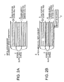
- FIG. 1 is an illustration for showing a configuration example of cells in a case where automatic lay-out is performed using a method of an embodiment of the present invention
- FIG. 2 A and FIG. 2B are arrangement diagrams for cells arranged using a primitive cell group of FIG. 1, and FIG. 2A shows a state of initial arrangement and FIG. 2B shows a state after wiring cells are arranged;
- FIG. 3 is a flowchart for explaining procedures of the present invention.
- FIG. 4 is an illustration for explaining a method for setting a new number of grids in a case where a set number of grids is excessive or insufficient;
- FIG. 5 A and FIG. 5B are illustrations for showing a cell arrangement and wiring cell replacement processing on data obtained after temporary wiring, and FIG. 5A shows a state before wiring-cell replacement and FIG. 5B shows a state after it;
- FIG. 6 A and FIG. 6B are illustrations for explaining another embodiment of the present invention, FIG. 6A shows a state before wiring-cell replacement and FIG. 6B shows a state after it; and
- FIG. 7 is an illustration for explaining a further embodiment of the present invention.
- FIG. 1 shows a configuration example of cells in a case where automatic lay-out is performed using a method of an embodiment of the present invention.
- a primitive cell group is divided into a core portion (core cell 102 ) in which a logic circuit is made up of transistors etc. and a power-supply wiring portion (wiring cell 101 ) in which a power-supply line and an inter-cell signal line are arranged.
- the wiring cell 101 is prepared as many as the number of mutually different numbers of grids, to sandwich the core cell 102 in arrangement. These cells constitute a primitive cell group used in the present invention.
- the number of grids shown in FIG. 1 is just one example and not restrictive.
- FIG. 2 An example of cell arrangement by use of the primitive cell group of FIG. 1 is shown in FIG. 2 .
- a core portion is there arranged a plurality of the core cells 102 to realize a certain function, above and below which is there arranged the wiring cell 101 having an arbitrary number of grids in arrangement (FIG. 2 A).
- a lay-out method of the present invention has a function to decide whether an arbitrarily set number of grids is excessive or insufficient using such a primitive cell group as described above, a function to calculate the number of grids that is optimal to a region, if any, of such excess or insufficiency, and a function to replace an initially arranged wiring cell with a wiring cell having a calculated number of grids.
- the process selects a plurality of wiring cells each containing an arbitrary number of grids (step 301 ).
- the process arranges the core cell 102 and the wiring cell 101 to perform connection processing for an inter-cell signal line. This connection processing is actually performed as many times as a selected number of grids (steps 302 and 303 ).
- the process extracts the number of the inter-cell signal lines passing through the wiring cell of data which has come up with a minimum lay-out area (step 304 ).
- the process compares the set number of grids and the extracted number of the inter-cell signal lines to each other (step 305 ) and, if the set number of grids is not excessive, immediately performs fine wiring and removes a wiring error (step 310 ).
- the process subtracts a predetermined number from the extracted number of grids (step 307 ).
- the predetermined number has been set preferably to three or less but is not restrictive in particular.
- the process performs this processing on each of such wiring cells 101 as to have an excessive or insufficient set number of grids (step 308 ) and replaces them with a wiring cell containing a newly set number of grids (step 309 ).
- the core cell 102 is not changed in arrangement but moved vertically by replacement of the wiring cells 101 .
- Data thus obtained undergoes fine wiring and wiring error removal (step 310 ) and, if no error is found, provides final data.
- the process identifies a wiring error location (step 312 ) and newly sets the number of grids which is larger, by one, than the number of grids contained in a wiring cell having this error (step 313 ) and then replaces this wiring cell with a cell containing the thus re-set number of grids (step 314 ).
- the process performs re-wiring and error removal on the error location and, if no more error is found, provides current data as final data. If another error is found, on the other hand, the process returns to a step of identification of an wiring error location (step 312 ), to repeat processing described below.
- a numerical value of six is set as the number of grids in initial setting (in which power-supply wiring portions 1 and 2 each have three grids), so that extraction of horizontal lines passing through the power-supply wiring portions 1 and 2 comes up with a result of one or two as the number of these horizontal lines.
- the process calculates a ratio of the number of the horizontal wiring lines being one and two in an area of the power-supply wiring portion 1 .
- the process re-sets the number of grids to the number of the wiring lines which has a ratio of 50% or more in the area.
- the number of the wiring lines which has a ratio of 50% or more is two, and in the power-supply wiring portion 2 , it is one. If no number of the wiring lines which has a ratio of 50% or more can be obtained, the process selects the number of the wiring lines which has a highest ratio as a processing subject.
- the process sets the number of grids which is smaller than a processing-subject number of the wiring lines by about one or two to then perform fine wiring. If an error still remains, to remove it, the process changes setting of the number of grids.
- the settings given here are just one example and those of the ratio and the number of grids can be changed.
- FIG. 5 shows a cell arrangement and wiring cell replacement processing on data obtained after temporary wiring.
- Data before wiring-cell replacement has five as an initially set number of wiring grids (three in the power-supply wiring portions 2 and 4 plus two in the power-supply wiring portions 1 and 3 ).
- the process utilizes operations of the present invention to extract horizontal wiring lines passing through the power-supply wiring portions 1 , 2 , 3 , and 4 and re-set the number of grids that matches each of the wiring cell regions; as a result of which, the wiring cells are replaced so that the number of grids may be changed from two to one in the power-supply wiring portion 1 , similarly, from three to two in the power-supply wiring portion 2 , from two to one in the power-supply wiring portion 3 , and from three to two in the power-supply wiring portion 4 .
- the necessary number of grids before wiring-cell replacement is a total of 10, whereas that after the replacement is a total of six, meaning a reduction of four grids of area in size.
- inter-cell signal line connection processing wiring processing
- spacing error or a short circuit error between one signal line and another or data in a core cell. If such an error cannot be removed in automatic lay-out wiring processing, the error can be removed using a method of the present invention.
- Processing of a step of wiring error location identification (step 312 ) and the subsequent in FIG. 3 corresponds to an error removing procedure according to this method of the present invention. It is also possible to use this method only for error removal.
- a power-supply wiring line and an inter-cell signal line short-circuit with each other at a boundary between the power-supply wiring portions 1 and 2 . This short circuit error is located using the present method to then replace the power-supply wiring portion 2 with a wiring cell having one more grid.
- a region can be specified to reduce the cell in size partially. This is actually possible by preparing, in addition to a wiring cell 1 , a wiring cell 2 for connection of a portion where a step has occurred, as power-supply wiring cells in a primitive cell group. Calculation processing performed here is the same as that described above.
- a chip size can be reduced if a region where core cells and wiring cells are arranged is reduced in area by replacing the wiring cells.
- automatic lay-out data undergoes wiring cell replacement and then fine wiring, so that a high-quality (high density) wiring result can be obtained.
Landscapes
- Engineering & Computer Science (AREA)
- Computer Hardware Design (AREA)
- Physics & Mathematics (AREA)
- Theoretical Computer Science (AREA)
- Evolutionary Computation (AREA)
- Geometry (AREA)
- General Engineering & Computer Science (AREA)
- General Physics & Mathematics (AREA)
- Design And Manufacture Of Integrated Circuits (AREA)
- Semiconductor Integrated Circuits (AREA)
Abstract
Description
Claims (9)
Applications Claiming Priority (3)
| Application Number | Priority Date | Filing Date | Title |
|---|---|---|---|
| JP363814/2001 | 2001-11-29 | ||
| JP2001-363814 | 2001-11-29 | ||
| JP2001363814A JP4010801B2 (en) | 2001-11-29 | 2001-11-29 | Automatic layout method of semiconductor integrated circuit |
Publications (2)
| Publication Number | Publication Date |
|---|---|
| US20030101424A1 US20030101424A1 (en) | 2003-05-29 |
| US6754880B2 true US6754880B2 (en) | 2004-06-22 |
Family
ID=19174094
Family Applications (1)
| Application Number | Title | Priority Date | Filing Date |
|---|---|---|---|
| US10/305,054 Expired - Fee Related US6754880B2 (en) | 2001-11-29 | 2002-11-27 | Method for automatically laying out semiconductor integrated circuit |
Country Status (2)
| Country | Link |
|---|---|
| US (1) | US6754880B2 (en) |
| JP (1) | JP4010801B2 (en) |
Families Citing this family (4)
| Publication number | Priority date | Publication date | Assignee | Title |
|---|---|---|---|---|
| DE102004038063A1 (en) * | 2004-07-30 | 2006-03-23 | Infineon Technologies Ag | Method for producing a standard cell arrangement and a device for carrying out the method |
| JP4492398B2 (en) * | 2005-03-16 | 2010-06-30 | 日本電気株式会社 | Integrated circuit layout design system and program |
| JP4983068B2 (en) * | 2006-03-30 | 2012-07-25 | 富士通株式会社 | Semiconductor device design support apparatus, semiconductor device design support method, and semiconductor device design support program |
| US8504967B2 (en) * | 2010-09-10 | 2013-08-06 | Apple Inc. | Configurable power switch cells and methodology |
Citations (2)
| Publication number | Priority date | Publication date | Assignee | Title |
|---|---|---|---|---|
| JPH11312185A (en) * | 1998-04-30 | 1999-11-09 | Nec Ic Microcomput Syst Ltd | Method for preparing layout data |
| JP2001007209A (en) | 1999-06-18 | 2001-01-12 | Nec Ic Microcomput Syst Ltd | Semiconductor integrated circuit device and layout method and device therefor |
-
2001
- 2001-11-29 JP JP2001363814A patent/JP4010801B2/en not_active Expired - Fee Related
-
2002
- 2002-11-27 US US10/305,054 patent/US6754880B2/en not_active Expired - Fee Related
Patent Citations (2)
| Publication number | Priority date | Publication date | Assignee | Title |
|---|---|---|---|---|
| JPH11312185A (en) * | 1998-04-30 | 1999-11-09 | Nec Ic Microcomput Syst Ltd | Method for preparing layout data |
| JP2001007209A (en) | 1999-06-18 | 2001-01-12 | Nec Ic Microcomput Syst Ltd | Semiconductor integrated circuit device and layout method and device therefor |
Also Published As
| Publication number | Publication date |
|---|---|
| US20030101424A1 (en) | 2003-05-29 |
| JP2003167934A (en) | 2003-06-13 |
| JP4010801B2 (en) | 2007-11-21 |
Similar Documents
| Publication | Publication Date | Title |
|---|---|---|
| US5483461A (en) | Routing algorithm method for standard-cell and gate-array integrated circuit design | |
| CN100394442C (en) | Semiconductor chip manufacturing execution system and method with recipe distribution management database | |
| US5682321A (en) | Cell placement method for microelectronic integrated circuit combining clustering, cluster placement and de-clustering | |
| JP4333770B2 (en) | Mask pattern creation program, semiconductor manufacturing method, mask pattern creation method, and semiconductor design program | |
| US8219959B2 (en) | Generating integrated circuit floorplan layouts | |
| US20040073878A1 (en) | Layout device | |
| EP0368625B1 (en) | Method and apparatus for forming layout pattern of semiconductor integrated circuit | |
| US6904575B2 (en) | Method for improving chip yields in the presence of via flaring | |
| US6754880B2 (en) | Method for automatically laying out semiconductor integrated circuit | |
| US6467070B2 (en) | Design support apparatus for semiconductor devices | |
| US20080115102A1 (en) | System and method for automatic elimination of connectivity mismatches during construction of a mask layout block, maintaining process design rule correctness | |
| JP2004070721A (en) | Automatic arrangement and wiring device | |
| CN110836905A (en) | A Failure Analysis Method for Automatic Identification of Chip Physical Defects | |
| US20070124714A1 (en) | Method for designing semiconductor integrated circuit layout | |
| US7698667B2 (en) | Pattern correction apparatus, pattern optimization apparatus, and integrated circuit design apparatus | |
| US7032207B2 (en) | Method of designing semiconductor integrated circuit with accurate capacitance extraction | |
| US8943453B2 (en) | Automatic application-rule checker | |
| US20070174793A1 (en) | Automatic design device, automatic design method, and automatic design program | |
| US20070266358A1 (en) | Yield calculation method | |
| Chiluvuri et al. | The effect of wire length minimization on yield | |
| US20050050504A1 (en) | Create modified view of existing IP so routing resources may be used if IP is not used and base layers will remain unchanged | |
| Wang et al. | Yield modeling of arbitrary defect outline | |
| JP4167413B2 (en) | Semiconductor device layout method | |
| TWI354901B (en) | Method, system, and article of manufacture for imp | |
| WO2009002302A1 (en) | System and method for automatic elimination of connectivity mismatches during construction of a mask layout block, maintaining the process design rules and layout connectivity correctness. |
Legal Events
| Date | Code | Title | Description |
|---|---|---|---|
| AS | Assignment |
Owner name: NEC ELECTRONICS CORPORATION, JAPAN Free format text: ASSIGNMENT OF ASSIGNORS INTEREST;ASSIGNOR:HAYAKAWA, MAYUMI;REEL/FRAME:013533/0725 Effective date: 20021121 |
|
| FEPP | Fee payment procedure |
Free format text: PAYOR NUMBER ASSIGNED (ORIGINAL EVENT CODE: ASPN); ENTITY STATUS OF PATENT OWNER: LARGE ENTITY |
|
| FPAY | Fee payment |
Year of fee payment: 4 |
|
| AS | Assignment |
Owner name: RENESAS ELECTRONICS CORPORATION, JAPAN Free format text: CHANGE OF NAME;ASSIGNOR:NEC ELECTRONICS CORPORATION;REEL/FRAME:025525/0163 Effective date: 20100401 |
|
| FPAY | Fee payment |
Year of fee payment: 8 |
|
| REMI | Maintenance fee reminder mailed | ||
| LAPS | Lapse for failure to pay maintenance fees | ||
| STCH | Information on status: patent discontinuation |
Free format text: PATENT EXPIRED DUE TO NONPAYMENT OF MAINTENANCE FEES UNDER 37 CFR 1.362 |
|
| STCH | Information on status: patent discontinuation |
Free format text: PATENT EXPIRED DUE TO NONPAYMENT OF MAINTENANCE FEES UNDER 37 CFR 1.362 |
|
| FP | Lapsed due to failure to pay maintenance fee |
Effective date: 20160622 |