US6746883B2 - Direct determination of interface traps in MOS devices - Google Patents
Direct determination of interface traps in MOS devices Download PDFInfo
- Publication number
- US6746883B2 US6746883B2 US10/064,036 US6403602A US6746883B2 US 6746883 B2 US6746883 B2 US 6746883B2 US 6403602 A US6403602 A US 6403602A US 6746883 B2 US6746883 B2 US 6746883B2
- Authority
- US
- United States
- Prior art keywords
- gate
- curve
- ultra
- low
- level
- Prior art date
- Legal status (The legal status is an assumption and is not a legal conclusion. Google has not performed a legal analysis and makes no representation as to the accuracy of the status listed.)
- Expired - Lifetime, expires
Links
- 230000005527 interface trap Effects 0.000 title claims abstract description 16
- 238000000034 method Methods 0.000 claims abstract description 40
- 238000005086 pumping Methods 0.000 claims abstract description 8
- 230000005641 tunneling Effects 0.000 claims abstract description 6
- 239000004065 semiconductor Substances 0.000 claims description 11
- 239000000758 substrate Substances 0.000 claims description 9
- VYPSYNLAJGMNEJ-UHFFFAOYSA-N Silicium dioxide Chemical compound O=[Si]=O VYPSYNLAJGMNEJ-UHFFFAOYSA-N 0.000 claims description 4
- 229910052814 silicon oxide Inorganic materials 0.000 claims description 4
- 238000012360 testing method Methods 0.000 claims description 3
- 238000011156 evaluation Methods 0.000 abstract 1
- 238000005259 measurement Methods 0.000 description 7
- IJGRMHOSHXDMSA-UHFFFAOYSA-N Atomic nitrogen Chemical compound N#N IJGRMHOSHXDMSA-UHFFFAOYSA-N 0.000 description 6
- 238000013459 approach Methods 0.000 description 5
- 230000000694 effects Effects 0.000 description 5
- 238000000605 extraction Methods 0.000 description 5
- 238000012512 characterization method Methods 0.000 description 3
- 230000001419 dependent effect Effects 0.000 description 3
- 238000009826 distribution Methods 0.000 description 3
- 229910052757 nitrogen Inorganic materials 0.000 description 3
- MWUXSHHQAYIFBG-UHFFFAOYSA-N Nitric oxide Chemical compound O=[N] MWUXSHHQAYIFBG-UHFFFAOYSA-N 0.000 description 2
- 230000002159 abnormal effect Effects 0.000 description 2
- 238000009825 accumulation Methods 0.000 description 2
- 239000003990 capacitor Substances 0.000 description 2
- 238000005516 engineering process Methods 0.000 description 2
- 230000004075 alteration Effects 0.000 description 1
- 230000015572 biosynthetic process Effects 0.000 description 1
- 238000004364 calculation method Methods 0.000 description 1
- 230000007423 decrease Effects 0.000 description 1
- 238000010586 diagram Methods 0.000 description 1
- 238000004519 manufacturing process Methods 0.000 description 1
- 239000000463 material Substances 0.000 description 1
- 238000012986 modification Methods 0.000 description 1
- 230000004048 modification Effects 0.000 description 1
- 238000005121 nitriding Methods 0.000 description 1
- 238000013441 quality evaluation Methods 0.000 description 1
- 238000007669 thermal treatment Methods 0.000 description 1
Images


Classifications
-
- G—PHYSICS
- G01—MEASURING; TESTING
- G01R—MEASURING ELECTRIC VARIABLES; MEASURING MAGNETIC VARIABLES
- G01R31/00—Arrangements for testing electric properties; Arrangements for locating electric faults; Arrangements for electrical testing characterised by what is being tested not provided for elsewhere
- G01R31/26—Testing of individual semiconductor devices
- G01R31/2607—Circuits therefor
- G01R31/2621—Circuits therefor for testing field effect transistors, i.e. FET's
-
- G—PHYSICS
- G01—MEASURING; TESTING
- G01R—MEASURING ELECTRIC VARIABLES; MEASURING MAGNETIC VARIABLES
- G01R31/00—Arrangements for testing electric properties; Arrangements for locating electric faults; Arrangements for electrical testing characterised by what is being tested not provided for elsewhere
- G01R31/26—Testing of individual semiconductor devices
- G01R31/2648—Characterising semiconductor materials
-
- G—PHYSICS
- G01—MEASURING; TESTING
- G01R—MEASURING ELECTRIC VARIABLES; MEASURING MAGNETIC VARIABLES
- G01R31/00—Arrangements for testing electric properties; Arrangements for locating electric faults; Arrangements for electrical testing characterised by what is being tested not provided for elsewhere
- G01R31/28—Testing of electronic circuits, e.g. by signal tracer
- G01R31/282—Testing of electronic circuits specially adapted for particular applications not provided for elsewhere
- G01R31/2831—Testing of materials or semi-finished products, e.g. semiconductor wafers or substrates
Definitions
- the present invention relates to semiconductor wafer testing. More particularly, this invention relates to characterization of semiconductor/oxide interface traps.
- a conventional approach to determining the interface traps in a gate oxide interface of a CMOS device is a Capacitance-Voltage (CV) method, which is proposed by Lewis M. Terman in 1962 (Solid-State Electronics, Vol.5(5), p.285-299, Lewis M. Terman, 1962).
- the prior art CV method is not able to extract accurate interface traps when the above-mentioned DTGL effect exists.
- the prior art CV method is not an effective approach to the oxide quality evaluation of an ultra-thin gate oxide device. Plus, the prior art CV method requires a large area capacitor structure such that it can not be applied to the measurement of real small MOS devices (with short channel length and narrow width).
- CP Charge-Pumping
- articles such as IEEE T-ED, Vol.36, p.1318-1335, P. Heremans et al., 1989; Proc. SSDM, p.841-843, S. S. Chung et al., 1993; IEEE T-ED, Vol.45, No.2, p.512-519, C. Chen et al., 1999; IEEE T-ED, Vol.46, p.1371-1377, S. S. Chung et al., 1999; and IEEE EDL, Vol.20, No.2, p.92-94, P. Masson et al., 1999.
- CP Charge-Pumping
- V gl fixed low-level gate voltage
- V gh increasing high
- FIG. 1 ( a ) schematically shows the fixed-based level pumping (GP) setup.
- FIG. 1 ( b ) schematically shows local threshold voltage (V TH ) and flat band (V fb ) distribution in relating to low level and high level gate voltage (V gl and V gh ), and normal and abnormal CP curves.
- FIG. 1 ( c ) is a flowchart according to this invention.
- FIG. 2 shows current components for FIG. 1 ( a ).
- FIG. 3 shows CP curves for a 16 ⁇ gate oxide device.
- FIG. 4 shows length dependent bulk currents.
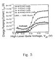
- FIG. 5 shows measured CP currents for an ultra-thin (12 ⁇ 16 ⁇ ) gate oxide layer.
- FIG. 6 shows High-low frequency CP method and Frequency dependent maximum CP currents.
- FIG. 7 shows Incremental frequency CP method and Frequency dependent maximum CP currents.
- FIG. 8 illustrates ⁇ L 0 extraction from CP data.
- FIG. 9 shows calculated N it and ⁇ L 0 from I CP,MAX in FIG. 7 .
- FIG. 10 illustrates Table 1 that shows the relating equations for determining the interface traps, N it that can be calculated from the I CP, MAX .
- the present invention is directed to a method for accurately determining interface traps (hereinafter referred to as N it ) in a semiconductor/oxide interface of advanced metal-oxide-semiconductor (MOS) devices having a short channel length and an ultra-thin gate oxide thereof.
- MOS devices to be tested are fabricated by state-of-the-art integrated circuit (IC) manufacturing techniques.
- IC integrated circuit
- a high-quality ultra-thin gate oxide layer having a thickness of about 12 ⁇ to 16 ⁇ (direct tunneling regime) is formed on a cleaned surface of a semiconductor substrate by using a known Rapid Thermal Nitric Oxide (RTNO) process.
- RTNO Rapid Thermal Nitric Oxide
- a Remote Plasma Nitridation (RFN) treatment is then used after the gate oxide formation for reducing the gate current leakage by a scale of about 2 to 3 orders.
- the masked lengths ranging from 0.22. m to 0.11. m are used.
- the RPN treatment is carried out in a suitable remote plasma tool that is commercially available from Applied Materials Corporation of Santa Clara, Calif.
- a wafer is placed in a second chamber located downstream from a first chamber so that species generated within the plasma pass over the wafer before being pumped out of the tool.
- Nitrogen is flowed into the plasma chamber at a flow rate of between about 600 and 3,000 sccm (Standard cubic centimeters per minute).
- NH 3 may be used, either instead of or in combination with nitrogen.
- the pumping rate of the tool is throttled to maintain a chamber pressure of between about 1 and 3 Torr in the second chamber.
- Plasma is struck in the first chamber and active nitrogen species from the remote plasma flow over the wafer surface and incorporate into the gate oxide, thereby nitriding an upper portion of the gate oxide.
- the RPN treatment is conducted with the wafer heated to a temperature between about 500° C. and 1,000° C. for a period of between about 3 and 5 minutes.
- FIG. 1 ( a ) is a schematic diagram of this invention.
- S/D source/drain
- V gl fixed base voltage
- I CP charge pumping current
- FIG. 2 shows experimental results of various current components of the measurement in FIG. 1 ( a ) wherein the gate current (I G ) is approximately equal to the combination of the drain current (I D ) and source current (I S ).
- FIG. 3 shows experimental results of CP curves. As shown in FIG. 2 and FIG. 3, obviously, leakage current occurs at a low V gh in the accumulation region. Accordingly, in a preferred embodiment of this invention, the configuration as depicted in FIG. 1 ( a ) is used for the CP measurement with a suitable chosen gate voltage.
- FIG. 1 ( b ) Please refer to FIG. 1 ( b ).
- V TH local threshold voltage
- V fb flat band
- V gl low-level gate voltage
- V gh high-level gate voltage
- eV ⁇ 1 The basic extraction equation for extracting N it (eV ⁇ 1 ) is demonstrated as follows:
- I CP MAX is maximum I CP of a characteristic (Amp.); “f” is frequency of gate pulse (Hz); “q” is electron charge (C); “W” is transistor width ( ⁇ m); “L” is channel length ( ⁇ m).
- the leakage component of I CP is very small at a low V gh when t ox >30 ⁇ . The leakage current becomes dominant when t ox is less than 20 ⁇ . It is believed that the leakage component of the bulk current comprises tunneling current and PN junction current.
- FIGS. 4 and 5 experimental results in accordance with the present invention are demonstrated.
- the bulk current (I B ) decreases with reducing channel length. This means that it is better to measure a low leakage I CP current with a shorter channel length device.
- the leakage current increases with reducing t ox (at V G ⁇ 0V).
- 12 ⁇ gate oxide has large leakage currents for V gh ⁇ 0V.
- FIG. 1 ( c ) is a flowchart showing the steps of this invention.
- a low leakage CP measurement window is chosen.
- a bulk current (I B ) of about 10 ⁇ 12 to 10 ⁇ amperes is suggested (also see FIG. 4 ).
- a fixed base level CP measurement is carried out. If a leakage component presents, the leakage component may be removed by either of the following steps:
- High-low frequency CP method First, the I CP currents for various frequencies are measured as shown in FIG. 6 . At a low gate pulse frequency, for example, 10 4 Hz, the group-2 curve (curve (2)) is considered as the leakage current. Curve (1) is the measured I CP at a high gate pulse frequency, for example, 1 MHz. A correct I CP (group-3 curve) is obtained by subtracting curve (2) from curve (1).
- Incremental frequency CP method From the measured I CP for various frequencies, the difference of I CP between two successive frequencies is taken as shown in FIG. 7 .
- I CP (1 MHz) ⁇ I CP (500 kHz) is regarded as the I CP at 500 kHz since I CP is directly proportional to f.
- FIG. 8 illustrates ⁇ L 0 extraction from I CP data.
- FIG. 8 (1) shows parameter definition and extraction method.
- FIG. 8 (2) shows interface traps distribution in short and long channel length devices respectively.
- FIG. 9 is a plot presenting calculated N it from I CP,MAX in FIG. 7 . It shows the extraction of offset length ⁇ L 0 ( ⁇ L 1 ( ⁇ 0.04 um)+ ⁇ L 2 ). As illustrated in FIG. 9, the calculated N it per unit width for the measured 80 devices with n- and p-channel are presented. It should be noted that: (1) a thicker gate oxide exhibits larger N it as a result of a longer thermal treatment, (2) RPN treated gate oxide has larger N it , and (3) the slopes of these curves give the N it values, which can be used as a monitor of the oxide quality.
- this invention provides a new CP methodology that is demonstrated for ultra-short channel length and ultra-thin gate oxide in the range 12 ⁇ to 16 ⁇ . It allows fast and easy calculation of the N it generated during the process. This method is superior to the conventional CV method for N it characterization in that the latter needs a large area capacitor samples.
- both the Incremental frequency CP method and the High-low frequency CP method can be applied to evaluate the hot carrier reliability in terms of the interface traps for deep sub-micron scale devices.
- the proposed method not only can be used to calculate the N it values but also be useful as a monitor of the oxide quality in an ultra-thin gate oxide process.
Landscapes
- Engineering & Computer Science (AREA)
- Microelectronics & Electronic Packaging (AREA)
- Physics & Mathematics (AREA)
- General Physics & Mathematics (AREA)
- Insulated Gate Type Field-Effect Transistor (AREA)
- Testing Of Individual Semiconductor Devices (AREA)
- Testing Or Measuring Of Semiconductors Or The Like (AREA)
Abstract
A low leakage charge pumping (CP) method has been implemented for direct determination of interface traps in ultra-short gate length MOS devices with ultra-thin gate oxide in the direct tunneling regime. The leakage current in a 12 Å-16 Å gate oxide can be removed from the measured CP current, which enables accurate determination of the interface traps. This method has been demonstrated successfully for variousRTNO grown and RPN treated oxide CMOS devices with very thin gate oxide. It can be used as a good monitor of ultra-thin gate oxide process and the evaluations of device reliabilities in relation to the interface trap generation. In addition, the current method can be used to determine the physical channel length of CMOS devices.
Description
1. Field of the Invention
The present invention relates to semiconductor wafer testing. More particularly, this invention relates to characterization of semiconductor/oxide interface traps.
2. Description of the Prior Art
Recently, semiconductor devices have been integrated so highly that integrated semiconductor devices have been designed on a nanometer level instead of a micron level (e.g., The National Technology Roadmap for Semiconductors Technology Needs, SIA, 2001 edition). In accordance with the SIA roadmap, by 2002, scaling of a sub-100 nm device will need a gate oxide thickness (tox) in the range of about 12 to 15 angstroms. However, this raises a thorny problem of how to evaluate quality of an ultra-thin gate oxide layer with a thickness of 10 to 20 angstroms in terms of interface traps (Nit).
As known by those skilled in the art, two pronounced effects are observed during testing of a MOS device as a gate oxide thickness shrinks down to 30 Å and below, namely, Direct Tunneling Gate Leakage (DTGL) effect and the so-called quantum mechanical effect. These effects render the device characterization more difficult.
A conventional approach to determining the interface traps in a gate oxide interface of a CMOS device is a Capacitance-Voltage (CV) method, which is proposed by Lewis M. Terman in 1962 (Solid-State Electronics, Vol.5(5), p.285-299, Lewis M. Terman, 1962). Unfortunately, the prior art CV method is not able to extract accurate interface traps when the above-mentioned DTGL effect exists. Obviously, the prior art CV method is not an effective approach to the oxide quality evaluation of an ultra-thin gate oxide device. Plus, the prior art CV method requires a large area capacitor structure such that it can not be applied to the measurement of real small MOS devices (with short channel length and narrow width).
Another prior art approach is a so-called Charge-Pumping (CP) method, which is disclosed in articles such as IEEE T-ED, Vol.36, p.1318-1335, P. Heremans et al., 1989; Proc. SSDM, p.841-843, S. S. Chung et al., 1993; IEEE T-ED, Vol.45, No.2, p.512-519, C. Chen et al., 1999; IEEE T-ED, Vol.46, p.1371-1377, S. S. Chung et al., 1999; and IEEE EDL, Vol.20, No.2, p.92-94, P. Masson et al., 1999. However, none of the prior art CP approaches generate an accurate and satisfactory result, in particular when the thickness of a tested gate oxide is less than 12 angstroms and beyond. Consequently, there is a strong need to provide an accurate approach to the measurement of Nit in the ultra-thin gate oxide age.
Accordingly, it is the primary objective of the claimed invention to provide an improved method for accurately characterizing semiconductor/oxide interface traps.
In accordance with the claimed invention, a method for determining interface traps in a semiconductor/oxide interface of a MOS transistor comprising a bulk substrate, a source, a drain, a gate, and a silicon oxide layer beneath the gate is provided. The method includes grounding the bulk substrate, source, and drain, applying a first gate pulse with a fixed low-level gate voltage (Vgl) and an increasing high-level gate voltage (Vgh) at a high gate pulse frequency on the gate so as to obtain a first charge-pumping current (ICP)−Vgh curve, applying a second gate pulse having same low-level gate voltage (Vgl) and same increasing high-level gate voltage (Vgh) as the first gate pulse at a lower gate pulse frequency on the gate so as to obtain a second ICP−Vgh curve, and subtracting the second ICP−Vgh curve from the first ICP−Vgh curve.
These and other objectives of the claimed invention will no doubt become obvious to those of ordinary skill in the art after reading the following detailed description of the preferred embodiment, which is illustrated in the various figures and drawings.
The accompanying drawings are included to provide a further understanding of the invention, and are incorporated in and constitute a part of this specification. The drawings illustrate embodiments of the invention and, together with the description, serve to explain the principles of the invention. In the drawings,
FIG. 1(a) schematically shows the fixed-based level pumping (GP) setup.
FIG. 1(b) schematically shows local threshold voltage (VTH) and flat band (Vfb) distribution in relating to low level and high level gate voltage (Vgl and Vgh), and normal and abnormal CP curves.
FIG. 1(c) is a flowchart according to this invention.
FIG. 2 shows current components for FIG. 1(a).
FIG. 3 shows CP curves for a 16 Å gate oxide device.
FIG. 4 shows length dependent bulk currents.
FIG. 5 shows measured CP currents for an ultra-thin (12˜16 Å) gate oxide layer.
FIG. 6 shows High-low frequency CP method and Frequency dependent maximum CP currents.
FIG. 7 shows Incremental frequency CP method and Frequency dependent maximum CP currents.
FIG. 8 illustrates ΔL0 extraction from CP data.
FIG. 9 shows calculated Nit and ΔL0 from ICP,MAX in FIG. 7.
FIG. 10 illustrates Table 1 that shows the relating equations for determining the interface traps, Nit that can be calculated from the ICP, MAX.
The present invention is directed to a method for accurately determining interface traps (hereinafter referred to as Nit) in a semiconductor/oxide interface of advanced metal-oxide-semiconductor (MOS) devices having a short channel length and an ultra-thin gate oxide thereof. The MOS devices to be tested are fabricated by state-of-the-art integrated circuit (IC) manufacturing techniques. For example, a high-quality ultra-thin gate oxide layer having a thickness of about 12 Å to 16 Å (direct tunneling regime) is formed on a cleaned surface of a semiconductor substrate by using a known Rapid Thermal Nitric Oxide (RTNO) process. In some cases, a Remote Plasma Nitridation (RFN) treatment is then used after the gate oxide formation for reducing the gate current leakage by a scale of about 2 to 3 orders. The masked lengths ranging from 0.22. m to 0.11. m are used.
By way of example, the RPN treatment is carried out in a suitable remote plasma tool that is commercially available from Applied Materials Corporation of Santa Clara, Calif. A wafer is placed in a second chamber located downstream from a first chamber so that species generated within the plasma pass over the wafer before being pumped out of the tool. In this manner, a gate oxide is not directly exposed to the plasma and therefore does not suffer plasma damage. Nitrogen is flowed into the plasma chamber at a flow rate of between about 600 and 3,000 sccm (Standard cubic centimeters per minute). Alternately NH3 may be used, either instead of or in combination with nitrogen. The pumping rate of the tool is throttled to maintain a chamber pressure of between about 1 and 3 Torr in the second chamber. Plasma is struck in the first chamber and active nitrogen species from the remote plasma flow over the wafer surface and incorporate into the gate oxide, thereby nitriding an upper portion of the gate oxide. The RPN treatment is conducted with the wafer heated to a temperature between about 500° C. and 1,000° C. for a period of between about 3 and 5 minutes.
Please refer to FIG. 1(a). FIG. 1(a) is a schematic diagram of this invention. Here, with both source/drain (S/D) grounded and by applying a gate pulse with fixed base voltage (Vgl), the channel operates between accumulation and inversion states. This gives rise to the charge pumping current (hereinafter referred to as ICP) measured from the bulk substrate.
Please refer to FIG. 2 and FIG. 3. FIG. 2 shows experimental results of various current components of the measurement in FIG. 1(a) wherein the gate current (IG) is approximately equal to the combination of the drain current (ID) and source current (IS). FIG. 3 shows experimental results of CP curves. As shown in FIG. 2 and FIG. 3, obviously, leakage current occurs at a low Vgh in the accumulation region. Accordingly, in a preferred embodiment of this invention, the configuration as depicted in FIG. 1(a) is used for the CP measurement with a suitable chosen gate voltage.
Please refer to FIG. 1(b). In the upper area of FIG. 1(b), local threshold voltage (VTH) and flat band (Vfb) distribution in relation to a low-level gate voltage (Vgl) and a high-level gate voltage (Vgh) is schematically shown. In the lower area of FIG. 1(b), correlation of normal and abnormal CP curves is demonstrated. The basic extraction equation for extracting Nit (eV−1) is demonstrated as follows:
where ICP, MAX is maximum ICP of a characteristic (Amp.); “f” is frequency of gate pulse (Hz); “q” is electron charge (C); “W” is transistor width (μm); “L” is channel length (μm). As seen in FIG. 1(b), the leakage component of ICP is very small at a low Vgh when tox>30 Å. The leakage current becomes dominant when tox is less than 20 Å. It is believed that the leakage component of the bulk current comprises tunneling current and PN junction current.
In FIGS. 4 and 5, experimental results in accordance with the present invention are demonstrated. As shown in FIG. 4 and FIG. 5, the bulk current (IB) decreases with reducing channel length. This means that it is better to measure a low leakage ICP current with a shorter channel length device. The leakage current increases with reducing tox (at VG<0V). In FIG. 5, note that 12 Å gate oxide has large leakage currents for Vgh<0V. Before calculating Nit from ICP, we need to remove the leakage current from the ICP.
Please refer to FIG. 1(c). FIG. 1(c) is a flowchart showing the steps of this invention. As shown in FIG. 1(c) with reference to FIG. 6 and FIG. 7, firstly, a low leakage CP measurement window is chosen. To choose a window for CP measurement, a bulk current (IB) of about 10−12 to 10−amperes is suggested (also see FIG. 4). Secondly, a fixed base level CP measurement is carried out. If a leakage component presents, the leakage component may be removed by either of the following steps:
(1) High-low frequency CP method: First, the ICP currents for various frequencies are measured as shown in FIG. 6. At a low gate pulse frequency, for example, 104 Hz, the group-2 curve (curve (2)) is considered as the leakage current. Curve (1) is the measured ICP at a high gate pulse frequency, for example, 1 MHz. A correct ICP (group-3 curve) is obtained by subtracting curve (2) from curve (1).
(2) Incremental frequency CP method: From the measured ICP for various frequencies, the difference of ICP between two successive frequencies is taken as shown in FIG. 7. For example, ICP (1 MHz)−ICP (500 kHz) is regarded as the ICP at 500 kHz since ICP is directly proportional to f.
When comparing curve (3) of FIG. 6 and curve (A) of FIG. 7, for example, both of the two steps give a close result of ICP for a 1 MHz signal. Since the leakage component is close at two successive frequencies, the incremental frequency CP method is expected to give more accurate results. As expected, even for very-thin (tox≦12 Å) gate oxide devices, this new CP methodology is still valid.
To determine the interface traps, Nit can be calculated from the ICP, MAX. The relating equations are given in Table 1. The definition and relating method are given in FIG. 8. FIG. 8 illustrates ΔL0 extraction from ICP data. FIG. 8 (1) shows parameter definition and extraction method. FIG. 8 (2) shows interface traps distribution in short and long channel length devices respectively.
FIG. 9 is a plot presenting calculated Nit from ICP,MAX in FIG. 7. It shows the extraction of offset length ΔL0 (≈ΔL1 (≈0.04 um)+ΔL2). As illustrated in FIG. 9, the calculated Nit per unit width for the measured 80 devices with n- and p-channel are presented. It should be noted that: (1) a thicker gate oxide exhibits larger Nit as a result of a longer thermal treatment, (2) RPN treated gate oxide has larger Nit, and (3) the slopes of these curves give the Nit values, which can be used as a monitor of the oxide quality.
In summary, this invention provides a new CP methodology that is demonstrated for ultra-short channel length and ultra-thin gate oxide in the range 12 Å to 16 Å. It allows fast and easy calculation of the Nit generated during the process. This method is superior to the conventional CV method for Nit characterization in that the latter needs a large area capacitor samples. On the other hand, both the Incremental frequency CP method and the High-low frequency CP method can be applied to evaluate the hot carrier reliability in terms of the interface traps for deep sub-micron scale devices. The proposed method not only can be used to calculate the Nit values but also be useful as a monitor of the oxide quality in an ultra-thin gate oxide process.
Those skilled in the art will readily observe that numerous modifications and alterations of the device may be made while retaining the teachings of the invention. Accordingly, the above disclosure should be construed as limited only by the metes and bounds of the appended claims.
Claims (8)
1. A method for determining interface traps in a semiconductor/oxide interface of a MOS transistor comprising a bulk substrate, a source, a drain, a gate, and a silicon oxide layer beneath the gate, the method comprising:
grounding the bulk substrate, source, and drain;
applying a first gate pulse having a fixed low-level gate voltage (Vgl) and an increasing high-level gate voltage (Vgh) at a high gate pulse frequency on the gate so as to obtain a first charge-pumping current ICP−Vgh curve;
applying a second gate pulse having the same low-level gate voltage (Vgl) and the same increasing high-level gate voltage (Vgh) as the first gate pulse at a low gate pulse frequency on the gate so as to obtain a second ICP−Vgh curve; and
subtracting the second ICP−Vgh curve from the first ICP−Vgh, curve.
2. The method of claim 1 wherein the second ICP−Vgh curve is approximately equal to a leakage current component.
3. The method of claim 1 wherein the silicon oxide layer has a thickness of less than 30 angstroms.
4. The method of claim 1 wherein the silicon oxide layer has a thickness that is in a direct tunneling regime.
5. The method of claim 1 wherein the high gate pulse frequency is about 1 MHz and the low gate pulse frequency is about 104 to 105 Hz.
6. A method for testing a MOS transistor having an ultra-thin gate oxide layer, wherein the MOS transistor comprises a bulk substrate, a source, a drain, a gate, and an ultra-thin gate oxide layer disposed between the gate and the bulk substrate, the method comprising:
grounding the bulk substrate, source, and drain, wherein the source and the drain are electrically connected to each other;
applying a first gate pulse having a fixed low-level gate voltage (Vgl) and an increasing high-level gate voltage (Vgh) at a high gate pulse frequency on the gate so as to obtain a first ICP−Vgh curve;
applying a second gate pulse having the same low-level gate voltage (Vgl) and the same increasing high-level gate voltage (Vgh) as the first gate pulse at a low gate pulse frequency on the gate so as to obtain a second ICP−Vgh curve; and
subtracting the second ICP−Vgh curve from the first ICP−Vgh curve so as to obtain a third ICP−Vgh curve that is regarded as a real charge-pumping current curve at the low gate pulse frequency.
7. The method of claim 6 wherein the ultra-thin gate oxide layer has a thickness of less than 20 angstroms.
8. The method of claim 6 wherein the ultra-thin gate oxide layer has a thickness that is in a direct tunneling regime.
Priority Applications (3)
| Application Number | Priority Date | Filing Date | Title |
|---|---|---|---|
| US10/064,036 US6746883B2 (en) | 2002-06-04 | 2002-06-04 | Direct determination of interface traps in MOS devices |
| CNB031002927A CN1312751C (en) | 2002-06-04 | 2003-01-10 | A Method of Directly Calculating the Defect Quantity at the Interface of Metal Oxygen Half Field Effect Transistor |
| CNB2005100682321A CN100377328C (en) | 2002-06-04 | 2003-01-10 | Method for directly calculating interface defect amount of metal oxide semiconductor field effect transistor |
Applications Claiming Priority (1)
| Application Number | Priority Date | Filing Date | Title |
|---|---|---|---|
| US10/064,036 US6746883B2 (en) | 2002-06-04 | 2002-06-04 | Direct determination of interface traps in MOS devices |
Publications (2)
| Publication Number | Publication Date |
|---|---|
| US20030224545A1 US20030224545A1 (en) | 2003-12-04 |
| US6746883B2 true US6746883B2 (en) | 2004-06-08 |
Family
ID=29581864
Family Applications (1)
| Application Number | Title | Priority Date | Filing Date |
|---|---|---|---|
| US10/064,036 Expired - Lifetime US6746883B2 (en) | 2002-06-04 | 2002-06-04 | Direct determination of interface traps in MOS devices |
Country Status (2)
| Country | Link |
|---|---|
| US (1) | US6746883B2 (en) |
| CN (2) | CN100377328C (en) |
Cited By (6)
| Publication number | Priority date | Publication date | Assignee | Title |
|---|---|---|---|---|
| US20070212800A1 (en) * | 2006-03-08 | 2007-09-13 | Macronix International Co., Ltd. | Methods for detecting charge effects during semiconductor processing |
| US20080096292A1 (en) * | 2006-10-20 | 2008-04-24 | Texas Instruments Incorporated | Method for measuring interface traps in thin gate oxide MOSFETs |
| RU2388110C1 (en) * | 2009-02-19 | 2010-04-27 | Федеральное государственное унитарное предприятие "НПО "ОРИОН" | Method of detecting hidden defects in matrix or linear mos multiplexers |
| RU2415493C1 (en) * | 2010-02-05 | 2011-03-27 | Российская Федерация, От Имени Которой Выступает Министерство Промышленности И Торговли Российской Федерации | Method to detect hidden defects of matrix or linear silicon mos multiplexor |
| CN104483615A (en) * | 2014-12-24 | 2015-04-01 | 上海华虹宏力半导体制造有限公司 | Trench gate MOS device defect verification method |
| US20150102831A1 (en) * | 2013-10-11 | 2015-04-16 | Gwanju Institute Of Science | Method of inspecting a semiconductor device and probing assembly for use therein |
Families Citing this family (10)
| Publication number | Priority date | Publication date | Assignee | Title |
|---|---|---|---|---|
| TW200423274A (en) * | 2003-04-25 | 2004-11-01 | United Microelectronics Corp | Method of measuring a gate channel length of a metal-oxide semiconductor transistor |
| US7737717B2 (en) * | 2008-03-05 | 2010-06-15 | Texas Instruments Incorporated | Current-voltage-based method for evaluating thin dielectrics based on interface traps |
| CN102520331B (en) * | 2011-12-02 | 2013-12-11 | 北京大学 | Interface trap testing method for shallow trench isolation (STI) type laterally diffused metal oxide semiconductor (LDMOS) device |
| CN104345259A (en) * | 2013-08-08 | 2015-02-11 | 北大方正集团有限公司 | Electric leakage position detection method of MOSFET (Metal-Oxide-Semiconductor Field Effect Transistor) |
| CN104101824B (en) * | 2014-07-24 | 2017-06-27 | 上海华力微电子有限公司 | The method of monitoring pattern chip gate oxidation layer surface |
| CN109001609B (en) * | 2018-07-17 | 2020-12-22 | 马丽娟 | Charge pump method for calculating stress-induced interface state density variation in nano CMOS device |
| CN109270423B (en) * | 2018-10-03 | 2020-11-20 | 大连理工大学 | A test method for evaluating the low temperature stability of SiC MOSFET devices |
| CN115097249B (en) * | 2022-07-19 | 2024-08-27 | 上海理工大学 | Method for detecting surface state defect of failure operational amplifier |
| CN116243132B (en) * | 2023-05-08 | 2023-10-24 | 长鑫存储技术有限公司 | Detection method, device and equipment |
| CN121487560A (en) * | 2026-01-08 | 2026-02-06 | 宁德时代润智软件科技有限公司 | Defect detection methods, apparatus, defect detection equipment, storage media and products |
Family Cites Families (6)
| Publication number | Priority date | Publication date | Assignee | Title |
|---|---|---|---|---|
| US3943442A (en) * | 1974-11-11 | 1976-03-09 | Nasa | Method and apparatus for measurement of trap density and energy distribution in dielectric films |
| JPH07153812A (en) * | 1993-11-29 | 1995-06-16 | Ricoh Co Ltd | Semiconductor device evaluation method, semiconductor device evaluation system, and semiconductor substrate |
| JPH08298274A (en) * | 1995-04-27 | 1996-11-12 | Oki Electric Ind Co Ltd | Evaluation method of interface level density of semiconductor element in lateral distribution |
| JPH10256327A (en) * | 1997-03-13 | 1998-09-25 | Mitsubishi Electric Corp | Evaluation method of semiconductor device |
| US6037797A (en) * | 1997-07-11 | 2000-03-14 | Semiconductor Diagnostics, Inc. | Measurement of the interface trap charge in an oxide semiconductor layer interface |
| US6391668B1 (en) * | 2000-05-01 | 2002-05-21 | Agere Systems Guardian Corp. | Method of determining a trap density of a semiconductor/oxide interface by a contactless charge technique |
-
2002
- 2002-06-04 US US10/064,036 patent/US6746883B2/en not_active Expired - Lifetime
-
2003
- 2003-01-10 CN CNB2005100682321A patent/CN100377328C/en not_active Expired - Lifetime
- 2003-01-10 CN CNB031002927A patent/CN1312751C/en not_active Expired - Lifetime
Non-Patent Citations (8)
| Title |
|---|
| C. Chen et al., IEEE T-ed, vol. 45, No. 2, 1999. |
| Lewis M. Terman, Solid-State Electronic, vol. 5(5), 1962, p. 285-299. |
| P. Heremans et al., IEEE T-ed, vol. 36, 1989, p. 1318-1335. |
| P. Masson et al., IEEE Ed1, vol. 20, No. 2, 1999, p. 92-94. |
| S.S. Chung et al., "A Novel and Direct Determination of the Interface Traps in Sub-100nm CMOS Devices with Direct Tunnelin Regime (12~16A) Gate Oxide," 2002 Symposium On VLSI Technology Digest of Technical Papers, pp. 74-75.* * |
| S.S. Chung et al., "A Novel and Direct Determination of the Interface Traps in Sub-100nm CMOS Devices with Direct Tunnelin Regime (12˜16A) Gate Oxide," 2002 Symposium On VLSI Technology Digest of Technical Papers, pp. 74-75.* |
| S.S. Chung et al., IEEE T-ed, vol. 46, 1999, p. 1371-1377. |
| S.S. Chung et al., Proc SSDM, 1993, p. 841-843. |
Cited By (7)
| Publication number | Priority date | Publication date | Assignee | Title |
|---|---|---|---|---|
| US20070212800A1 (en) * | 2006-03-08 | 2007-09-13 | Macronix International Co., Ltd. | Methods for detecting charge effects during semiconductor processing |
| US20080096292A1 (en) * | 2006-10-20 | 2008-04-24 | Texas Instruments Incorporated | Method for measuring interface traps in thin gate oxide MOSFETs |
| RU2388110C1 (en) * | 2009-02-19 | 2010-04-27 | Федеральное государственное унитарное предприятие "НПО "ОРИОН" | Method of detecting hidden defects in matrix or linear mos multiplexers |
| RU2415493C1 (en) * | 2010-02-05 | 2011-03-27 | Российская Федерация, От Имени Которой Выступает Министерство Промышленности И Торговли Российской Федерации | Method to detect hidden defects of matrix or linear silicon mos multiplexor |
| US20150102831A1 (en) * | 2013-10-11 | 2015-04-16 | Gwanju Institute Of Science | Method of inspecting a semiconductor device and probing assembly for use therein |
| CN104483615A (en) * | 2014-12-24 | 2015-04-01 | 上海华虹宏力半导体制造有限公司 | Trench gate MOS device defect verification method |
| CN104483615B (en) * | 2014-12-24 | 2017-10-24 | 上海华虹宏力半导体制造有限公司 | Trench grate MOS device defect verification method |
Also Published As
| Publication number | Publication date |
|---|---|
| CN1691303A (en) | 2005-11-02 |
| CN100377328C (en) | 2008-03-26 |
| CN1312751C (en) | 2007-04-25 |
| US20030224545A1 (en) | 2003-12-04 |
| CN1466184A (en) | 2004-01-07 |
Similar Documents
| Publication | Publication Date | Title |
|---|---|---|
| US6746883B2 (en) | Direct determination of interface traps in MOS devices | |
| Vogel et al. | Limitations of conductance to the measurement of the interface state density of MOS capacitors with tunneling gate dielectrics | |
| Ogawa et al. | Interface‐trap generation at ultrathin SiO2 (4–6 nm)‐Si interfaces during negative‐bias temperature aging | |
| Graffeuil et al. | Analysis of capacitance and transconductance frequency dispersions in MESFETs for surface characterization | |
| US6251697B1 (en) | Non-contact method for monitoring and controlling plasma charging damage in a semiconductor device | |
| Islam et al. | Mobility degradation due to interface traps in plasma oxynitride PMOS devices | |
| Zeitzoff et al. | Correcting effective mobility measurements for the presence of significant gate leakage current | |
| US20080096292A1 (en) | Method for measuring interface traps in thin gate oxide MOSFETs | |
| Fang et al. | Oxide damage from plasma charging: Breakdown mechanism and oxide quality | |
| Ling et al. | A study of hot carrier degradation in NMOSEET's by gate capacitance and charge pumping current | |
| Tsai et al. | 1/f noise in hot-carrier damaged MOSFET's: effects of oxide charge and interface traps | |
| Wright et al. | Nitridation and post-nitridation anneals of SiO/sub 2/for ultrathin dielectrics | |
| Schroder | Electrical characterization of defects in gate dielectrics | |
| US5904490A (en) | Method of measuring electron shading damage | |
| Weintraub et al. | Study of low-frequency charge pumping on thin stacked dielectrics | |
| Noguchi et al. | The effect of plasma-induced oxide and interface degradation on hot carrier reliability | |
| Neugroschel et al. | Measurement of the interface trap and dielectric charge density in high-/spl kappa/gate stacks | |
| US6731130B1 (en) | Method of determining gate oxide thickness of an operational MOSFET | |
| Redondo et al. | Thermally induced improvements on SiN x: H/InP devices | |
| Frutuoso et al. | Fast CV MSM Technique for Comprehensive Analysis of Bulk Trapping in Low-K Carbon-Doped Dielectrics | |
| Simoen et al. | Empirical relationship between the low‐frequency noise spectral density and the transconductance of silicon‐on‐insulator n‐channel metal‐oxide‐semiconductor transistors | |
| US6815974B1 (en) | Determining composition of mixed dielectrics | |
| US7548067B2 (en) | Methods for measuring capacitance | |
| Seng et al. | Investigation of PMOS Transistor Threshold Voltage Shift in BCD Technology | |
| Chindalore et al. | An experimental study of the effect of quantization on the effective electrical oxide thickness in MOS electron and hole accumulation layers in heavily doped Si |
Legal Events
| Date | Code | Title | Description |
|---|---|---|---|
| AS | Assignment |
Owner name: UNITED MICROELECTRONICS CORP., TAIWAN Free format text: ASSIGNMENT OF ASSIGNORS INTEREST;ASSIGNORS:CHUNG, STEVE S.;CHEN, SHANG-JR;YANG, CHIEN-KUO;AND OTHERS;REEL/FRAME:012765/0729 Effective date: 20020520 |
|
| STCF | Information on status: patent grant |
Free format text: PATENTED CASE |
|
| FPAY | Fee payment |
Year of fee payment: 4 |
|
| FPAY | Fee payment |
Year of fee payment: 8 |
|
| FPAY | Fee payment |
Year of fee payment: 12 |