US6743707B2 - Bump fabrication process - Google Patents
Bump fabrication process Download PDFInfo
- Publication number
- US6743707B2 US6743707B2 US10/248,163 US24816302A US6743707B2 US 6743707 B2 US6743707 B2 US 6743707B2 US 24816302 A US24816302 A US 24816302A US 6743707 B2 US6743707 B2 US 6743707B2
- Authority
- US
- United States
- Prior art keywords
- layer
- conductive layer
- bonding pads
- photoresist layer
- portions
- Prior art date
- Legal status (The legal status is an assumption and is not a legal conclusion. Google has not performed a legal analysis and makes no representation as to the accuracy of the status listed.)
- Expired - Lifetime
Links
Images


Classifications
-
- H—ELECTRICITY
- H10—SEMICONDUCTOR DEVICES; ELECTRIC SOLID-STATE DEVICES NOT OTHERWISE PROVIDED FOR
- H10W—GENERIC PACKAGES, INTERCONNECTIONS, CONNECTORS OR OTHER CONSTRUCTIONAL DETAILS OF DEVICES COVERED BY CLASS H10
- H10W72/00—Interconnections or connectors in packages
- H10W72/01—Manufacture or treatment
- H10W72/012—Manufacture or treatment of bump connectors, dummy bumps or thermal bumps
-
- H—ELECTRICITY
- H10—SEMICONDUCTOR DEVICES; ELECTRIC SOLID-STATE DEVICES NOT OTHERWISE PROVIDED FOR
- H10W—GENERIC PACKAGES, INTERCONNECTIONS, CONNECTORS OR OTHER CONSTRUCTIONAL DETAILS OF DEVICES COVERED BY CLASS H10
- H10W72/00—Interconnections or connectors in packages
- H10W72/01—Manufacture or treatment
- H10W72/019—Manufacture or treatment of bond pads
-
- H—ELECTRICITY
- H10—SEMICONDUCTOR DEVICES; ELECTRIC SOLID-STATE DEVICES NOT OTHERWISE PROVIDED FOR
- H10W—GENERIC PACKAGES, INTERCONNECTIONS, CONNECTORS OR OTHER CONSTRUCTIONAL DETAILS OF DEVICES COVERED BY CLASS H10
- H10W72/00—Interconnections or connectors in packages
- H10W72/01—Manufacture or treatment
- H10W72/012—Manufacture or treatment of bump connectors, dummy bumps or thermal bumps
- H10W72/01221—Manufacture or treatment of bump connectors, dummy bumps or thermal bumps using local deposition
- H10W72/01223—Manufacture or treatment of bump connectors, dummy bumps or thermal bumps using local deposition in liquid form, e.g. by dispensing droplets or by screen printing
-
- H—ELECTRICITY
- H10—SEMICONDUCTOR DEVICES; ELECTRIC SOLID-STATE DEVICES NOT OTHERWISE PROVIDED FOR
- H10W—GENERIC PACKAGES, INTERCONNECTIONS, CONNECTORS OR OTHER CONSTRUCTIONAL DETAILS OF DEVICES COVERED BY CLASS H10
- H10W72/00—Interconnections or connectors in packages
- H10W72/01—Manufacture or treatment
- H10W72/012—Manufacture or treatment of bump connectors, dummy bumps or thermal bumps
- H10W72/01251—Changing the shapes of bumps
- H10W72/01255—Changing the shapes of bumps by using masks
-
- H—ELECTRICITY
- H10—SEMICONDUCTOR DEVICES; ELECTRIC SOLID-STATE DEVICES NOT OTHERWISE PROVIDED FOR
- H10W—GENERIC PACKAGES, INTERCONNECTIONS, CONNECTORS OR OTHER CONSTRUCTIONAL DETAILS OF DEVICES COVERED BY CLASS H10
- H10W72/00—Interconnections or connectors in packages
- H10W72/01—Manufacture or treatment
- H10W72/019—Manufacture or treatment of bond pads
- H10W72/01951—Changing the shapes of bond pads
- H10W72/01955—Changing the shapes of bond pads by using masks
-
- H—ELECTRICITY
- H10—SEMICONDUCTOR DEVICES; ELECTRIC SOLID-STATE DEVICES NOT OTHERWISE PROVIDED FOR
- H10W—GENERIC PACKAGES, INTERCONNECTIONS, CONNECTORS OR OTHER CONSTRUCTIONAL DETAILS OF DEVICES COVERED BY CLASS H10
- H10W72/00—Interconnections or connectors in packages
- H10W72/20—Bump connectors, e.g. solder bumps or copper pillars; Dummy bumps; Thermal bumps
- H10W72/241—Dispositions, e.g. layouts
- H10W72/242—Dispositions, e.g. layouts relative to the surface, e.g. recessed, protruding
-
- H—ELECTRICITY
- H10—SEMICONDUCTOR DEVICES; ELECTRIC SOLID-STATE DEVICES NOT OTHERWISE PROVIDED FOR
- H10W—GENERIC PACKAGES, INTERCONNECTIONS, CONNECTORS OR OTHER CONSTRUCTIONAL DETAILS OF DEVICES COVERED BY CLASS H10
- H10W72/00—Interconnections or connectors in packages
- H10W72/20—Bump connectors, e.g. solder bumps or copper pillars; Dummy bumps; Thermal bumps
- H10W72/251—Materials
- H10W72/252—Materials comprising solid metals or solid metalloids, e.g. PbSn, Ag or Cu
-
- H—ELECTRICITY
- H10—SEMICONDUCTOR DEVICES; ELECTRIC SOLID-STATE DEVICES NOT OTHERWISE PROVIDED FOR
- H10W—GENERIC PACKAGES, INTERCONNECTIONS, CONNECTORS OR OTHER CONSTRUCTIONAL DETAILS OF DEVICES COVERED BY CLASS H10
- H10W72/00—Interconnections or connectors in packages
- H10W72/20—Bump connectors, e.g. solder bumps or copper pillars; Dummy bumps; Thermal bumps
- H10W72/29—Bond pads specially adapted therefor
-
- H—ELECTRICITY
- H10—SEMICONDUCTOR DEVICES; ELECTRIC SOLID-STATE DEVICES NOT OTHERWISE PROVIDED FOR
- H10W—GENERIC PACKAGES, INTERCONNECTIONS, CONNECTORS OR OTHER CONSTRUCTIONAL DETAILS OF DEVICES COVERED BY CLASS H10
- H10W72/00—Interconnections or connectors in packages
- H10W72/90—Bond pads, in general
- H10W72/951—Materials of bond pads
Definitions
- the present invention relates to a fabrication process for forming bumps. More particularly, the present invention relates to the lift-off technology for forming the under bump metallurgy layer in the bump fabrication process.
- the integrated circuit (IC) packaging needs to be improved following the developing trends of electronic devices such as digitalization, network localization, and user friendliness.
- electronic devices In order to meet the above requirements, electronic devices must have multiple functions and high integration, and maintain high operating speed, miniaturization, lightweight, and low cost.
- High-density packages such as ball grid arrays (BGAs), chip scale packages (CSPs), flip chips, and multi-chip modules (MCMs) have been developed.
- BGAs ball grid arrays
- CSPs chip scale packages
- MCMs multi-chip modules
- the integrated circuit packaging density is determined by the degree of numbers of pins per area unit. For high-density IC packaging, the signal transmitting speed increases as the wiring length decreases. Thus, the application of bumps has become the main trend in the high-density packaging.
- FIGS. 1-7 are cross-sectional views illustrating a conventional fabrication process for forming bumps.
- a wafer 100 is provided with a bonding pad 102 and a protective layer 104 .
- the protective layer 104 protects a surface of the wafer and exposes a surface of the bonding pad 102 .
- a photoresist layer 106 having an opening 108 is formed over the wafer 100 .
- the location of the opening 108 corresponds to the locations of the bonding pad 102 , so as to expose the surface of the bonding pad 102 .
- the opening 108 has a structure similar to an undercut (an undercut structure), for example.
- a conductive layer 109 is formed over the wafer 100 covered with the photoresist layer 106 .
- the conductive layer 109 includes an adhesion layer 110 a, a barrier layer 110 b, and a wetting (solder) layer 110 c. Because of the photoresist layer, the adhesion layer 110 a, the barrier layer 110 b and the wetting (solder) layer 110 c are located on both the bonding pad 102 and the photoresist layer 106 . On the other hand, the adhesion layer 110 a, the barrier layer 110 b and the wetting layer 110 c are not present on sidewalls of the opening 108 .
- the photoresist layer 106 is stripped along with the adhesion layer 110 a, the barrier layer 110 b and the wetting layer 110 c on the photoresist layer 106 . Therefore, after stripping the photoresist layer, the adhesion layer 110 a, the barrier layer 110 b and the wetting layer 110 c remaining on the bonding pad 102 becomes an under bump metallurgy (UBM) layer 110 .
- UBM under bump metallurgy
- a photoresist layer 112 is formed over the wafer 100 with an opening 114 .
- the opening 114 corresponds to the UBM layer 110 , thus exposing the UBM layer 110 .
- a solder paste 116 is filled into the opening 114 of the photoresist layer 112 by electroplating or screen printing.
- the photoresist layer 112 is stripped and a reflow step is performed, so that the solder paste 116 becomes a globular bump 118 .
- one mask process further includes dehydration bake, priming, soft bake, exposure, post exposure bake, development, hard bake and etching.
- one extra mask process can greatly increase the production cost for the bumps.
- the present invention provides a bump fabrication process by using the lift-off technology for lifting off the conductive layer on the photoresist layer, so that the photoresist layer can be used to further define the formation locations of bumps, thus saving one mask process.
- the bump fabrication process of the present invention comprises the following steps.
- a wafer is provided with a patterned photoresist layer formed on the wafer.
- the patterned photoresist layer has a plurality of openings that expose bonding pads on the wafer.
- a conductive layer is formed on the photoresist layer and the exposed bonding pads.
- a sticker film is provided to peel off the conductive layer on the photoresist layer, while the conductive layer within the openings is not removed.
- a solder paste is filled Into the openings.
- a reflow step is performed to turn the solder paste filled in the openings into globular bumps.
- the ball mounting method is used to form bumps.
- the photoresist layer is removed.
- the adhesion between the film and the conductive layer is stronger than the adhesion between the conductive layer and the photoresist layer.
- the sticker film is, for example, an adhesive tape or other mechanism that can peel the conductive layer from the photoresist layer.
- the conductive layer is a stacked layer comprising an adhesive layer, a barrier layer and a wetting layer.
- the conductive layer comprises a layer selected from the following group consisting of a titanium-tungsten/nickel-vanadium/copper layer, an aluminum/nickel-vanadium/copper layer, a titanium/nickel-vanadium/copper layer, and a chromium/nickel-vanadium/copper layer.
- the conductive layer should be easily peeled by the sticker film, while the conductive layer adheres well to the bonding pads.
- FIGS. 1-7 are cross-sectional views illustrating a conventional fabrication process for forming bumps.
- FIGS. 8-14 are cross-sectional views illustrating steps of a bump fabrication process according to one preferred embodiment of this invention.
- FIGS. 8-14 are cross-sectional views illustrating steps of a bump fabrication process according to one preferred embodiment of this invention.
- a substrate or wafer 200 is provided with a bonding pad 202 and a protective (passivation) layer 204 .
- the protective layer 204 is disposed on the wafer 200 , protecting a surface of the wafer 200 and exposing a surface of the bonding pad 202 .
- the bonding pad 202 can be an aluminum pad or a copper pad, for example.
- a photoresist layer 206 having an opening 208 is formed over the wafer 200 .
- the location of the opening 208 corresponds to the location of the bonding pad 202 , so as to expose the surface of the bonding pad 202 .
- the opening 208 has a structure similar to an undercut (an undercut structure), for example.
- a conductive layer 209 is formed over the wafer 200 and on the photoresist layer 206 .
- the conductive layer 209 includes an adhesion layer 210 a, a barrier layer 210 b, and a wetting (solder) layer 210 c. Due to the pattern (opening) of the photoresist layer, the adhesion layer 210 a, the barrier layer 210 b and the wetting (solder) layer 210 c are located on both the bonding pad 202 and the photoresist layer 206 . On the other hand, the adhesion layer 210 a, the barrier layer 210 b and the wetting layer 210 c are not present on sidewalls of the opening 208 . That is, the conductive layer 209 (the adhesion layer 210 a, the barrier layer 210 b and the wetting layer 210 c ) is disconnected because of the interruption of the opening 208 .
- a sticker film 212 for example, an adhesive tape, is formed on the wetting layer 210 c.
- the sticker film 212 is adhered to the wetting layer 210 c, so as to lift the adhesion layer 210 a, the barrier layer 210 b and the wetting layer 210 c that are situated on the photoresist layer 206 from the photoresist layer 206 . Therefore, after lifting off the conductive layer 209 from the photoresist layer 206 , the adhesion layer 210 a, the barrier layer 210 b and the wetting layer 210 c remaining on the bonding pad 202 becomes an under bump metallurgy (UBM) layer 210 .
- UBM under bump metallurgy
- the adhesion between the sticker film 212 and the wetting layer 210 c must be stronger than the adhesion between the adhesion layer 210 a and the photoresist layer 206 . Therefore, the material of the adhesion layer 210 a is preferably chosen to have weaker adhesion toward the photoresist layer 206 . Depending on the materials of the adhesion layer 210 a, various materials can be used for forming the barrier layer 210 b and the wetting layer 210 c.
- the UBM layer 210 can be a stacked layer of titanium-tungsten/nickel-vanadium/copper (TiW/NiV/Cu), chromium/nickel-vanadium/copper (Cr/NiV/Cu), aluminum/nickel-vanadium/copper (Al/NiV/Cu), or titanium/nickel-vanadium/copper (Ti/NiV/Cu), for example.
- TiW/NiV/Cu titanium-tungsten/nickel-vanadium/copper
- Cr/NiV/Cu chromium/nickel-vanadium/copper
- Al/NiV/Cu aluminum/nickel-vanadium/copper
- Ti/NiV/Cu titanium/nickel-vanadium/copper
- the photoresist layer 206 after peeling the adhesion layer 210 a, the barrier layer 210 b and the wetting layer 210 c from the photoresist layer 206 , the photoresist layer 206 remains over the wafer 200 with the opening 208 .
- the opening 208 exposing the UBM layer 210 , corresponds to the formation location of the bump. Therefore, the photoresist layer 206 can be further used to define the location for subsequently forming the bump.
- a solder paste 214 is filled into the opening 208 of the photoresist layer 206 by, for example, electroplating, screen printing or other technology. There is no misalignment issue occurring because the same photoresist layer 206 defines the UBM layer 210 and the location filled by the solder paste 214 .
- the photoresist layer 206 is removed. After removing the photoresist layer 206 , a reflow step is performed to turn the filled solder paste 214 into a globular bump 216 Alternatively, the ball mounting method can be used to form bumps and a reflow step is performed to fix the bumps.
- the bump fabrication process of the present invention has at least the following advantages:
- the photoresist layer is retained and can be used again in the following process of solder paste filling.
- the same photoresist layer is used to define the UBM layer and the location filled by the solder paste, thus reducing one extra mask process (another photoresist layer).
Landscapes
- Wire Bonding (AREA)
- Internal Circuitry In Semiconductor Integrated Circuit Devices (AREA)
Abstract
The present invention provides a bump fabrication process. A wafer is provided with a patterned photoresist layer formed on the wafer. The patterned photoresist layer has a plurality of openings, corresponding to bonding pads. A conductive layer is formed on the photoresist layer and the exposed bonding pads. Afterwards, a sticker film is the provided to lift off the conductive layer on the photoresist layer, while the conductive layer within the openings is not removed. A solder paste is filled into the openings. A reflow step is performed to turn the filled solder paste into globular bumps. At last, the protoresist layer is removed.
Description
This application claims the priority benefit of Taiwan application serial no. 90133197, filed Dec. 31, 2001.
1. Field of Invention
The present invention relates to a fabrication process for forming bumps. More particularly, the present invention relates to the lift-off technology for forming the under bump metallurgy layer in the bump fabrication process.
2. Description of Related Art
At present, the market of multimedia applications rapidly expands. The integrated circuit (IC) packaging needs to be improved following the developing trends of electronic devices such as digitalization, network localization, and user friendliness. In order to meet the above requirements, electronic devices must have multiple functions and high integration, and maintain high operating speed, miniaturization, lightweight, and low cost. High-density packages, such as ball grid arrays (BGAs), chip scale packages (CSPs), flip chips, and multi-chip modules (MCMs) have been developed. The integrated circuit packaging density is determined by the degree of numbers of pins per area unit. For high-density IC packaging, the signal transmitting speed increases as the wiring length decreases. Thus, the application of bumps has become the main trend in the high-density packaging.
FIGS. 1-7 are cross-sectional views illustrating a conventional fabrication process for forming bumps. Referring to the FIG. 1, a wafer 100 is provided with a bonding pad 102 and a protective layer 104. The protective layer 104 protects a surface of the wafer and exposes a surface of the bonding pad 102.
Referring to FIG. 2, a photoresist layer 106 having an opening 108 is formed over the wafer 100. The location of the opening 108 corresponds to the locations of the bonding pad 102, so as to expose the surface of the bonding pad 102. The opening 108 has a structure similar to an undercut (an undercut structure), for example.
Referring to FIG. 3, a conductive layer 109 is formed over the wafer 100 covered with the photoresist layer 106. The conductive layer 109 includes an adhesion layer 110 a, a barrier layer 110 b, and a wetting (solder) layer 110 c. Because of the photoresist layer, the adhesion layer 110 a, the barrier layer 110 b and the wetting (solder) layer 110 c are located on both the bonding pad 102 and the photoresist layer 106. On the other hand, the adhesion layer 110 a, the barrier layer 110 b and the wetting layer 110 c are not present on sidewalls of the opening 108.
Referring to FIG. 4, the photoresist layer 106 is stripped along with the adhesion layer 110 a, the barrier layer 110 b and the wetting layer 110 c on the photoresist layer 106. Therefore, after stripping the photoresist layer, the adhesion layer 110 a, the barrier layer 110 b and the wetting layer 110 c remaining on the bonding pad 102 becomes an under bump metallurgy (UBM) layer 110.
Referring to FIG. 5, after forming the UBM layer 110 on the bonding pad 102, a photoresist layer 112 is formed over the wafer 100 with an opening 114. The opening 114 corresponds to the UBM layer 110, thus exposing the UBM layer 110.
Referring to FIG. 6, a solder paste 116 is filled into the opening 114 of the photoresist layer 112 by electroplating or screen printing.
Referring to FIG. 7, after filling the solder paste, the photoresist layer 112 is stripped and a reflow step is performed, so that the solder paste 116 becomes a globular bump 118.
In the conventional bump fabrication process, the adhesion layer, the barrier layer and the wetting layer on the photoresist layer are removed with the photoresist layer. Subsequently, another mask process is required to define the locations of bump formation. Usually, one mask process further includes dehydration bake, priming, soft bake, exposure, post exposure bake, development, hard bake and etching. Thus, one extra mask process can greatly increase the production cost for the bumps.
The present invention provides a bump fabrication process by using the lift-off technology for lifting off the conductive layer on the photoresist layer, so that the photoresist layer can be used to further define the formation locations of bumps, thus saving one mask process.
Accordingly, the bump fabrication process of the present invention comprises the following steps. A wafer is provided with a patterned photoresist layer formed on the wafer. The patterned photoresist layer has a plurality of openings that expose bonding pads on the wafer. A conductive layer is formed on the photoresist layer and the exposed bonding pads. Afterwards, a sticker film is provided to peel off the conductive layer on the photoresist layer, while the conductive layer within the openings is not removed. A solder paste is filled Into the openings. A reflow step is performed to turn the solder paste filled in the openings into globular bumps. Alternatively, the ball mounting method is used to form bumps. At last, the photoresist layer is removed.
As embodied and broadly described herein, the adhesion between the film and the conductive layer is stronger than the adhesion between the conductive layer and the photoresist layer. The sticker film is, for example, an adhesive tape or other mechanism that can peel the conductive layer from the photoresist layer.
The conductive layer is a stacked layer comprising an adhesive layer, a barrier layer and a wetting layer.
As embodied and broadly described herein, the conductive layer comprises a layer selected from the following group consisting of a titanium-tungsten/nickel-vanadium/copper layer, an aluminum/nickel-vanadium/copper layer, a titanium/nickel-vanadium/copper layer, and a chromium/nickel-vanadium/copper layer. However, the conductive layer should be easily peeled by the sticker film, while the conductive layer adheres well to the bonding pads.
It is to be understood that both the foregoing general description and the following detailed description are exemplary, and are intended to provide further explanation of the invention as claimed.
The accompanying drawings are included to provide a further understanding of the invention, and are incorporated in and constitute a part of this specification. The drawings illustrate embodiments of the invention and, together with the description, serve to explain the principles of the invention. In the drawings,
FIGS. 1-7 are cross-sectional views illustrating a conventional fabrication process for forming bumps; and
FIGS. 8-14 are cross-sectional views illustrating steps of a bump fabrication process according to one preferred embodiment of this invention.
FIGS. 8-14 are cross-sectional views illustrating steps of a bump fabrication process according to one preferred embodiment of this invention.
Referring to the FIG. 8, a substrate or wafer 200 is provided with a bonding pad 202 and a protective (passivation) layer 204. The protective layer 204 is disposed on the wafer 200, protecting a surface of the wafer 200 and exposing a surface of the bonding pad 202. The bonding pad 202 can be an aluminum pad or a copper pad, for example.
As shown in FIG. 9, a photoresist layer 206 having an opening 208 is formed over the wafer 200. The location of the opening 208 corresponds to the location of the bonding pad 202, so as to expose the surface of the bonding pad 202. The opening 208 has a structure similar to an undercut (an undercut structure), for example.
Referring to FIG. 10, a conductive layer 209 is formed over the wafer 200 and on the photoresist layer 206. The conductive layer 209 includes an adhesion layer 210 a, a barrier layer 210 b, and a wetting (solder) layer 210 c. Due to the pattern (opening) of the photoresist layer, the adhesion layer 210 a, the barrier layer 210 b and the wetting (solder) layer 210 c are located on both the bonding pad 202 and the photoresist layer 206. On the other hand, the adhesion layer 210 a, the barrier layer 210 b and the wetting layer 210 c are not present on sidewalls of the opening 208. That is, the conductive layer 209 (the adhesion layer 210 a, the barrier layer 210 b and the wetting layer 210 c) is disconnected because of the interruption of the opening 208.
Referring to FIG. 11, a sticker film 212, for example, an adhesive tape, is formed on the wetting layer 210 c. The sticker film 212 is adhered to the wetting layer 210 c, so as to lift the adhesion layer 210 a, the barrier layer 210 b and the wetting layer 210 c that are situated on the photoresist layer 206 from the photoresist layer 206. Therefore, after lifting off the conductive layer 209 from the photoresist layer 206, the adhesion layer 210 a, the barrier layer 210 b and the wetting layer 210 c remaining on the bonding pad 202 becomes an under bump metallurgy (UBM) layer 210. The adhesion between the sticker film 212 and the wetting layer 210 c must be stronger than the adhesion between the adhesion layer 210 a and the photoresist layer 206. Therefore, the material of the adhesion layer 210 a is preferably chosen to have weaker adhesion toward the photoresist layer 206. Depending on the materials of the adhesion layer 210 a, various materials can be used for forming the barrier layer 210 b and the wetting layer 210 c. In the preferred embodiment, the UBM layer 210 can be a stacked layer of titanium-tungsten/nickel-vanadium/copper (TiW/NiV/Cu), chromium/nickel-vanadium/copper (Cr/NiV/Cu), aluminum/nickel-vanadium/copper (Al/NiV/Cu), or titanium/nickel-vanadium/copper (Ti/NiV/Cu), for example.
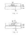
Referring to FIG. 12, after peeling the adhesion layer 210 a, the barrier layer 210 b and the wetting layer 210 c from the photoresist layer 206, the photoresist layer 206 remains over the wafer 200 with the opening 208. The opening 208, exposing the UBM layer 210, corresponds to the formation location of the bump. Therefore, the photoresist layer 206 can be further used to define the location for subsequently forming the bump.
Referring to FIG. 13, a solder paste 214 is filled into the opening 208 of the photoresist layer 206 by, for example, electroplating, screen printing or other technology. There is no misalignment issue occurring because the same photoresist layer 206 defines the UBM layer 210 and the location filled by the solder paste 214.
Referring to FIG. 14, after filling the solder paste 214, the photoresist layer 206 is removed. After removing the photoresist layer 206, a reflow step is performed to turn the filled solder paste 214 into a globular bump 216 Alternatively, the ball mounting method can be used to form bumps and a reflow step is performed to fix the bumps.
In conclusion, the bump fabrication process of the present invention has at least the following advantages:
(1)By using the sticker film to remove the adhesion layer, the barrier layer and the wetting layer from the photoresist layer, the photoresist layer is retained and can be used again in the following process of solder paste filling.
(2)In the bump fabrication process of the present invention, the same photoresist layer is used to define the UBM layer and the location filled by the solder paste, thus reducing one extra mask process (another photoresist layer).
(3)There is no misalignment issue because the same photoresist layer defines the UBM layer and the location filled by the solder paste.
It will be apparent to those skilled in the art that various modifications and variations can be made to the structure of the present invention without departing from the scope or spirit of the invention. In view of the foregoing, it is intended that the present invention cover modifications and variations of this invention provided they fall within the scope of the following claims and their equivalents.
Claims (10)
1. A bump fabrication process, comprising:
providing a wafer with a surface having a plurality of bonding pads and a passivation layer thereon, wherein the passivation layer covers the surface and exposes the bonding pads;
forming a photoresist layer having a plurality of openings over the wafer, wherein the openings correspond to the bonding pads;
forming at least a conductive layer on the bonding pads and the photoresist layer, wherein portions of the conductive layer are on the photoresist layer and other portions of the conductive layer are on the bonding pads, and the portions and the other portions of the conductive layer are on different levels above the wafer;
forming a film on the portions of the conductive layer on the photoresist layer;
lifting off the film so as to remove the conductive layer from the photoresist layer and leave the other portions of the conductive layer on the bonding pads;
forming a plurality of bumps on the bonding pads by filling a solder into each of the openings;
performing a reflow step to fix the bumps onto the bonding pads; and
removing the photoresist layer.
2. The process of claim 1 , wherein the film comprises an adhesive tape.
3. The process of claim 1 , wherein a first adhesion between the film and the conductive layer is stronger than a second adhesion between the conductive layer and the photoresist layer.
4. The process of claim 1 , wherein the conductive layer comprises an adhesive layer, a barrier layer and a wetting layer.
5. The process of claim 1 , wherein the conductive layer comprises a layer selected from the following group consisting of a titanium-tungsten/nickel-vanadium/copper layer, an aluminum/nickel-vanadium/copper layer, a titanium/nickel-vanadium/copper layer, and a chromium/nickel-vanadium/copper layer.
6. A method for forming an under bump metallurgy (UBM) layer, comprising:
providing a wafer with a surface having a plurality of bonding pads and a passivation layer thereon, wherein the passivation layer covers the surface and exposes the bonding pads;
forming a photoresist layer having a plurality of openings over the wafer, wherein the openings correspond to the bonding pads;
forming at least a conductive layer on the bonding pads and the photoresist layer, wherein portions of the conductive layer are on the photoresist layer and other portions of the conductive layer are on the bonding pads, and the portions and the other portions of the conductive layer are on different levels above the wafer;
forming a film on the portions of the conductive layer on the photoresist layer; and
lifting off the film so as to remove the conductive layer from the photoresist layer and leave the other portions of the conductive layer on the bonding pads.
7. The method of claim 6 , wherein the film comprises an adhesive tape.
8. The method of claim 6 , wherein a first adhesion between the film and the conductive layer is stronger than a second adhesion between the conductive layer and the photoresist layer.
9. The method of claim 6 , wherein the conductive layer comprises an adhesive layer, a barrier layer and a wetting layer.
10. The method of claim 6 , wherein the conductive layer comprises a layer selected from the following group consisting of a titanium-tungsten/nickel-vanadium/copper layer, an aluminum/nickel-vanadium/copper layer, a titanium/nickel-vanadium/copper layer, and a chromium/nickel-vanadium/copper layer.
Applications Claiming Priority (3)
| Application Number | Priority Date | Filing Date | Title |
|---|---|---|---|
| TW090133197A TWI243439B (en) | 2001-12-31 | 2001-12-31 | Bumping process |
| TW90133197A | 2001-12-31 | ||
| TW90133197 | 2001-12-31 |
Publications (2)
| Publication Number | Publication Date |
|---|---|
| US20030124833A1 US20030124833A1 (en) | 2003-07-03 |
| US6743707B2 true US6743707B2 (en) | 2004-06-01 |
Family
ID=21680124
Family Applications (1)
| Application Number | Title | Priority Date | Filing Date |
|---|---|---|---|
| US10/248,163 Expired - Lifetime US6743707B2 (en) | 2001-12-31 | 2002-12-23 | Bump fabrication process |
Country Status (2)
| Country | Link |
|---|---|
| US (1) | US6743707B2 (en) |
| TW (1) | TWI243439B (en) |
Cited By (2)
| Publication number | Priority date | Publication date | Assignee | Title |
|---|---|---|---|---|
| US20050077626A1 (en) * | 2003-10-13 | 2005-04-14 | Jacky Seiller | Forming of the last metallization level of an integrated circuit |
| TWI381504B (en) * | 2009-10-16 | 2013-01-01 | Powertech Technology Inc | Method for forming metal bumps |
Families Citing this family (15)
| Publication number | Priority date | Publication date | Assignee | Title |
|---|---|---|---|---|
| AU2002228926A1 (en) | 2000-11-10 | 2002-05-21 | Unitive Electronics, Inc. | Methods of positioning components using liquid prime movers and related structures |
| US6863209B2 (en) | 2000-12-15 | 2005-03-08 | Unitivie International Limited | Low temperature methods of bonding components |
| US7531898B2 (en) | 2002-06-25 | 2009-05-12 | Unitive International Limited | Non-Circular via holes for bumping pads and related structures |
| US7547623B2 (en) | 2002-06-25 | 2009-06-16 | Unitive International Limited | Methods of forming lead free solder bumps |
| WO2004001837A2 (en) | 2002-06-25 | 2003-12-31 | Unitive International Limited | Methods of forming electronic structures including conductive shunt layers and related structures |
| TWI225899B (en) | 2003-02-18 | 2005-01-01 | Unitive Semiconductor Taiwan C | Etching solution and method for manufacturing conductive bump using the etching solution to selectively remove barrier layer |
| CN1291069C (en) * | 2003-05-31 | 2006-12-20 | 香港科技大学 | Electroplating preparation method of fine-pitch flip-chip bumps |
| WO2005101499A2 (en) * | 2004-04-13 | 2005-10-27 | Unitive International Limited | Methods of forming solder bumps on exposed metal pads and related structures |
| US20080003715A1 (en) * | 2006-06-30 | 2008-01-03 | Lee Kevin J | Tapered die-side bumps |
| US7585615B2 (en) * | 2006-07-27 | 2009-09-08 | Intel Corporation | Composite photoresist for modifying die-side bumps |
| US7713861B2 (en) * | 2007-10-13 | 2010-05-11 | Wan-Ling Yu | Method of forming metallic bump and seal for semiconductor device |
| DE102009013921B3 (en) | 2009-03-19 | 2010-09-30 | Forschungsverbund Berlin E.V. | Method for producing a metallization for at least one contact pad and semiconductor wafer with metallization for at least one contact pad |
| US8492892B2 (en) * | 2010-12-08 | 2013-07-23 | International Business Machines Corporation | Solder bump connections |
| CN106876254B (en) * | 2017-03-14 | 2019-05-28 | 京东方科技集团股份有限公司 | Array substrate, display device, thin film transistor and preparation method of film pattern |
| CN111554581A (en) * | 2020-04-07 | 2020-08-18 | 厦门通富微电子有限公司 | A process for forming a conductive column and a package body |
Citations (10)
| Publication number | Priority date | Publication date | Assignee | Title |
|---|---|---|---|---|
| JPS6045041A (en) * | 1983-08-22 | 1985-03-11 | Nec Corp | Semiconductor device and manufacture thereof |
| US4514751A (en) * | 1982-12-23 | 1985-04-30 | International Business Machines Corporation | Compressively stresses titanium metallurgy for contacting passivated semiconductor devices |
| JPH03171631A (en) * | 1989-11-29 | 1991-07-25 | Toshiba Corp | Formation of bump electrode |
| US5384283A (en) * | 1993-12-10 | 1995-01-24 | International Business Machines Corporation | Resist protection of ball limiting metal during etch process |
| US5496770A (en) * | 1993-02-08 | 1996-03-05 | Samsung Electronics Co., Ltd. | Method for manufacturing a semiconductor chip bump having improved contact characteristics |
| US5631499A (en) * | 1994-04-28 | 1997-05-20 | Kabushiki Kaisha Toshiba | Semiconductor device comprising fine bump electrode having small side etch portion and stable characteristics |
| US5846875A (en) * | 1996-08-20 | 1998-12-08 | Matsushita Electric Industrial Co., Ltd. | Method of producing a semiconductor device |
| US5903058A (en) * | 1996-07-17 | 1999-05-11 | Micron Technology, Inc. | Conductive bumps on die for flip chip application |
| US6452270B1 (en) * | 2000-10-13 | 2002-09-17 | Advanced Semiconductor Engineering, Inc. | Semiconductor device having bump electrode |
| US6548386B1 (en) * | 1999-05-17 | 2003-04-15 | Denso Corporation | Method for forming and patterning film |
-
2001
- 2001-12-31 TW TW090133197A patent/TWI243439B/en not_active IP Right Cessation
-
2002
- 2002-12-23 US US10/248,163 patent/US6743707B2/en not_active Expired - Lifetime
Patent Citations (10)
| Publication number | Priority date | Publication date | Assignee | Title |
|---|---|---|---|---|
| US4514751A (en) * | 1982-12-23 | 1985-04-30 | International Business Machines Corporation | Compressively stresses titanium metallurgy for contacting passivated semiconductor devices |
| JPS6045041A (en) * | 1983-08-22 | 1985-03-11 | Nec Corp | Semiconductor device and manufacture thereof |
| JPH03171631A (en) * | 1989-11-29 | 1991-07-25 | Toshiba Corp | Formation of bump electrode |
| US5496770A (en) * | 1993-02-08 | 1996-03-05 | Samsung Electronics Co., Ltd. | Method for manufacturing a semiconductor chip bump having improved contact characteristics |
| US5384283A (en) * | 1993-12-10 | 1995-01-24 | International Business Machines Corporation | Resist protection of ball limiting metal during etch process |
| US5631499A (en) * | 1994-04-28 | 1997-05-20 | Kabushiki Kaisha Toshiba | Semiconductor device comprising fine bump electrode having small side etch portion and stable characteristics |
| US5903058A (en) * | 1996-07-17 | 1999-05-11 | Micron Technology, Inc. | Conductive bumps on die for flip chip application |
| US5846875A (en) * | 1996-08-20 | 1998-12-08 | Matsushita Electric Industrial Co., Ltd. | Method of producing a semiconductor device |
| US6548386B1 (en) * | 1999-05-17 | 2003-04-15 | Denso Corporation | Method for forming and patterning film |
| US6452270B1 (en) * | 2000-10-13 | 2002-09-17 | Advanced Semiconductor Engineering, Inc. | Semiconductor device having bump electrode |
Cited By (3)
| Publication number | Priority date | Publication date | Assignee | Title |
|---|---|---|---|---|
| US20050077626A1 (en) * | 2003-10-13 | 2005-04-14 | Jacky Seiller | Forming of the last metallization level of an integrated circuit |
| US7919864B2 (en) * | 2003-10-13 | 2011-04-05 | Stmicroelectronics S.A. | Forming of the last metallization level of an integrated circuit |
| TWI381504B (en) * | 2009-10-16 | 2013-01-01 | Powertech Technology Inc | Method for forming metal bumps |
Also Published As
| Publication number | Publication date |
|---|---|
| TWI243439B (en) | 2005-11-11 |
| US20030124833A1 (en) | 2003-07-03 |
Similar Documents
| Publication | Publication Date | Title |
|---|---|---|
| US6743707B2 (en) | Bump fabrication process | |
| US6489185B1 (en) | Protective film for the fabrication of direct build-up layers on an encapsulated die package | |
| US6964889B2 (en) | Method to protect an encapsulated die package during back grinding with a solder metallization layer and devices formed thereby | |
| KR100320648B1 (en) | Wafer level chip scale package and process for making the same | |
| US6593220B1 (en) | Elastomer plating mask sealed wafer level package method | |
| TWI317548B (en) | Chip structure and method for fabricating the same | |
| US6605525B2 (en) | Method for forming a wafer level package incorporating a multiplicity of elastomeric blocks and package formed | |
| CN100426492C (en) | Direct build-up layer on encapsulated die package | |
| US6372619B1 (en) | Method for fabricating wafer level chip scale package with discrete package encapsulation | |
| US7565737B2 (en) | Manufacturing method of package substrate | |
| US20020070443A1 (en) | Microelectronic package having an integrated heat sink and build-up layers | |
| US6696317B1 (en) | Method of manufacturing a flip-chip semiconductor device with a stress-absorbing layer made of thermosetting resin | |
| US6664128B2 (en) | Bump fabrication process | |
| US6930031B2 (en) | Bumping process | |
| EP1941541B1 (en) | Redistribution layer for wafer-level chip scale package and method therefor | |
| US7189646B2 (en) | Method of enhancing the adhesion between photoresist layer and substrate and bumping process | |
| US6444561B1 (en) | Method for forming solder bumps for flip-chip bonding by using perpendicularly laid masking strips | |
| KR100691000B1 (en) | Manufacturing Method of Wafer Level Package | |
| US20040259345A1 (en) | Formation method of conductive bump | |
| JP2000195890A (en) | Method for manufacturing semiconductor device | |
| JP2004072043A (en) | Semiconductor wafer, semiconductor chip, semiconductor device and method of manufacturing the same | |
| US20060049518A1 (en) | Semiconductor device and method for manufacturing the same | |
| US20050181538A1 (en) | Semiconductor device for wire-bonding and flip-chip bonding package and manufacturing method thereof | |
| US6713320B2 (en) | Bumping process | |
| US20070218675A1 (en) | Method for manufacturing bump of wafer level package |
Legal Events
| Date | Code | Title | Description |
|---|---|---|---|
| AS | Assignment |
Owner name: ADVANCED SEMICONDUCTOR ENGINEERING, INC., TAIWAN Free format text: ASSIGNMENT OF ASSIGNORS INTEREST;ASSIGNORS:TONG, HO-MING;LEE, CHUN-CHI;FANG, JEN-KUANG;AND OTHERS;REEL/FRAME:013309/0615;SIGNING DATES FROM 20021028 TO 20021105 |
|
| STCF | Information on status: patent grant |
Free format text: PATENTED CASE |
|
| FPAY | Fee payment |
Year of fee payment: 4 |
|
| REMI | Maintenance fee reminder mailed | ||
| FPAY | Fee payment |
Year of fee payment: 8 |
|
| FPAY | Fee payment |
Year of fee payment: 12 |