US6741356B1 - Method for detecting physical amount of object and optical apparatus using the same - Google Patents
Method for detecting physical amount of object and optical apparatus using the same Download PDFInfo
- Publication number
- US6741356B1 US6741356B1 US09/664,723 US66472300A US6741356B1 US 6741356 B1 US6741356 B1 US 6741356B1 US 66472300 A US66472300 A US 66472300A US 6741356 B1 US6741356 B1 US 6741356B1
- Authority
- US
- United States
- Prior art keywords
- image information
- optical system
- image
- amount
- light source
- Prior art date
- Legal status (The legal status is an assumption and is not a legal conclusion. Google has not performed a legal analysis and makes no representation as to the accuracy of the status listed.)
- Expired - Lifetime, expires
Links
Images
Classifications
-
- G—PHYSICS
- G01—MEASURING; TESTING
- G01B—MEASURING LENGTH, THICKNESS OR SIMILAR LINEAR DIMENSIONS; MEASURING ANGLES; MEASURING AREAS; MEASURING IRREGULARITIES OF SURFACES OR CONTOURS
- G01B9/00—Measuring instruments characterised by the use of optical techniques
- G01B9/04—Measuring microscopes
-
- G—PHYSICS
- G01—MEASURING; TESTING
- G01B—MEASURING LENGTH, THICKNESS OR SIMILAR LINEAR DIMENSIONS; MEASURING ANGLES; MEASURING AREAS; MEASURING IRREGULARITIES OF SURFACES OR CONTOURS
- G01B9/00—Measuring instruments characterised by the use of optical techniques
- G01B9/02—Interferometers
- G01B9/02015—Interferometers characterised by the beam path configuration
- G01B9/02024—Measuring in transmission, i.e. light traverses the object
-
- G—PHYSICS
- G01—MEASURING; TESTING
- G01B—MEASURING LENGTH, THICKNESS OR SIMILAR LINEAR DIMENSIONS; MEASURING ANGLES; MEASURING AREAS; MEASURING IRREGULARITIES OF SURFACES OR CONTOURS
- G01B9/00—Measuring instruments characterised by the use of optical techniques
- G01B9/02—Interferometers
- G01B9/02083—Interferometers characterised by particular signal processing and presentation
- G01B9/02087—Combining two or more images of the same region
-
- G—PHYSICS
- G02—OPTICS
- G02B—OPTICAL ELEMENTS, SYSTEMS OR APPARATUS
- G02B21/00—Microscopes
- G02B21/06—Means for illuminating specimens
- G02B21/08—Condensers
- G02B21/14—Condensers affording illumination for phase-contrast observation
-
- G—PHYSICS
- G01—MEASURING; TESTING
- G01B—MEASURING LENGTH, THICKNESS OR SIMILAR LINEAR DIMENSIONS; MEASURING ANGLES; MEASURING AREAS; MEASURING IRREGULARITIES OF SURFACES OR CONTOURS
- G01B2290/00—Aspects of interferometers not specifically covered by any group under G01B9/02
- G01B2290/70—Using polarization in the interferometer
Definitions
- This invention relates to a method for detecting a step and a phase change of an object to be observed from the image information of the object obtained by an interference microscope such as a differential interference contrast microscope (DIC microscope), and an optical apparatus using the method.
- an interference microscope such as a differential interference contrast microscope (DIC microscope)
- DIC microscope differential interference contrast microscope
- a microscope utilizing interference such as a DIC microscope
- a DIC microscope has been widely used to observe the microscopic structure of a human body or an IC pattern because information on a phase change and a step of an object can be visualized by interference.
- various attempts have recently been made to use the DIC microscope for the inspection of minute projections (bumps) for intimate contact prevention of a magnetic head, provided on the surface of a magnetic disk, the measurements of a defect in a phase-shift reticle used for pattern exposure of a semiconductor and the amount of phase difference, and the positioning device of a semiconductor wafer.
- minute projections bump
- each of Japanese Patent Preliminary Publication Nos. Hei 5-149719 and Hei 7-248261 discloses a technique of applying a DIC microscope, which is thought of as a shearing interferometer or a Mach-Zehnder interferometer, to the detection of a defect in a phase-shift reticle and the measurement of phase.
- Japanese Patent Preliminary Publication No. Hei 7-239212 discloses a technique that the DIC microscope is used to detect the edge of a positioning mark provided on a semiconductor wafer, thereby positioning the semiconductor wafer.
- the DIC microscope is such that a phase change on the surface of the object is converted into an image intensity distribution.
- the intensity distribution of a differential interference contrast image is analyzed and thereby the phase change on the surface of the object can be detected.
- Japanese Patent Preliminary Publication No. Hei 5-256795 discloses a technique that uses the differential interference contrast image of a normal sample as a reference image and compares this reference image with the image of the object, thereby detecting foreign matter contained in the object.
- a Michelson type or Mirau type interference microscope is also used to measure the phase distribution of the object.
- the phase change of the object cannot be detected with accuracy if the object contains factors other than the phase change of the object caused by a change in transmittance or reflectance of light or a change in intensity of illumination light in the object.
- a fringe scanning technique employed for interference measurement is combined with the operation of the DIC microscope and thereby the phase information of the object can be extracted.
- the fringe scanning technique four images in which the amounts of retardation between polarized components are different must be formed for calculation, and thus the problem of reducing a processing time cannot be solved.
- an object of the present invention to provide a method for detecting the height of a step and the amount of phase change of an object in a shorter time than in a conventional way and making a precise measurement when the height of the step increases, by separating phase information and intensity information from an interference image of the object obtained by an interference microscope, and a detection apparatus (optical apparatus) using this method.
- the detection apparatus includes a microscope optical system having a light source, an illumination optical system for leading light emitted from the light source to an object, an imaging optical system for forming the image of the object, and at least one polarizing member for separating the light from the light source into two polarized components; an adjusting member for changing the amount of retardation between the two polarized components; and an image pickup member for photographing a differential interference contrast image of the object.
- the detection apparatus operated through a process for photographing two differential interference contrast images relative to the object in which the amounts of retardation are equal, but have different signs, is provided with a processing unit operated through a calculation process for performing a differential calculation and a s ed calculation relative to respective pixels corresponding to the two differential interference contrast images to obtain differential image information and summed image information and another calculation process for detecting the amount of phase on the surface of the object by using one of the following equations:
- ⁇ ( x,y ) k ⁇ (1 ⁇ cos ⁇ ) ⁇ d ( x,y )/ ⁇ / ⁇ sin ⁇ [1 ⁇ d ( x,y )/ ⁇ 2 /2] ⁇
- ⁇ ( x,y ) k ⁇ tan ⁇ 1 [ ⁇ (1 ⁇ cos ⁇ ) ⁇ d ( x,y )/ ⁇ / ⁇ sin ⁇ [1 ⁇ d ( x,y )/ ⁇ 2 /2] ⁇ ]
- ⁇ is the amount of retardation
- ⁇ (x,y) is the amount of phase on the surface of the object corresponding to the differential image information and the summed image information
- D(x,y) is image information in which the differential image information D(x,y) is deconvoluted by using the optical transfer function of the microscope optical system
- ⁇ is the average value of the summed image information S(x,y)
- k ⁇ /4 ⁇ ; where ⁇ is a wavelength.
- the detection apparatus includes an interference optical system having a light source, an illumination optical path for leading light emitted from the light source to an object, and a reference optical path for leading the light from the light source to a reference surface; and an image pick-up member for photographing an interference image of the object formed by the interference optical system.
- the detection apparatus is provided with a processing unit operated through a calculation process for detecting the amount of phase on the surface of the object by using one of the following equations:
- ⁇ ( x,y ) k ⁇ h ( x,y )/ Jm ( x,y ) ⁇ / ⁇ [1 ⁇ h ( x,y )/ Jm ( x,y ) ⁇ 2 /2] ⁇
- ⁇ ( x,y ) k ⁇ tan ⁇ 1 [k ⁇ h ( x,y )/ Jm ( x,y ) ⁇ / ⁇ [1 ⁇ h ( x,y )/ Jm ( x,y ) ⁇ 2 /2] ⁇ ]
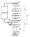
- FIG. 1 is a view showing the construction of an apparatus for detecting the physical amount of an object in the present invention
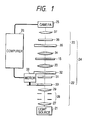
- FIG. 2 is a graph showing the optical transfer function of a DIC microscope
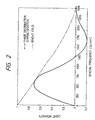
- FIGS. 3A and 3B are photographs showing differential interference contrast images relative to the object where the apparatus of FIG. 1 is used and the amounts of retardation between polarized components obtained by a method according to a first embodiment are ⁇ and ⁇ , respectively;
- FIGS. 3C and 3D are photographs showing a differential image and a summed image which are formed from the images of FIGS. 3A and 3B, respectively;
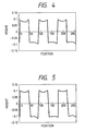
- FIG. 4 is a view showing the reproduction of a phase distribution in the present invention.
- FIG. 5 is a view showing the reproduction of a phase distribution detected by a conventional fringe scanning technique
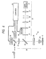
- FIG. 6 is a view showing another example of an apparatus for detecting the physical amount of the object in the present invention.
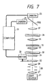
- FIG. 7 is a view showing still another example of an apparatus for detecting the physical amount of an object in the present invention.
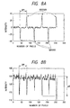
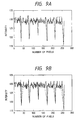
- FIGS. 8A and 8B are diagrams showing intensity distributions of the images of FIGS. 3C and 3D, respectively;
- FIGS. 9A and 9B are diagrams showing envelopes which are obtained by connecting the maxima and minima, respectively, of the intensity distribution of FIG. 8B;
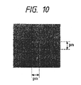
- FIG. 10 is a view showing a technique of dividing an image as a region.
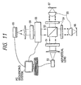
- FIG. 11 is a view showing schematically the construction of an apparatus used for a method of finding a correct phase distribution in the present invention.
- the detection apparatus of the present invention includes a DIC microscope having a light source, an illumination optical system for introducing light emitted from the light source into an object to be observed, provided with a member for splitting the light from the light source into two polarized components, and an imaging optical system for forming an image of the object, provided with a member for recombining the two polarized components split in the illumination optical system; an adjusting member for changing the amount of retardation between the two polarized components; an image pick-up member for photographing the image of the object; and a processing unit for performing a calculation with respect to the image captured by this image pick-up member.
- amounts of retardation between the two polarized components split in the illumination optical system are detected to form two differential interference contrast images relative to the object in which the amounts of retardation between the polarized components are equal, but have different signs.
- a differential calculation and a summed calculation are performed with regard to respective corresponding pixels to obtain a differential image and a summed image.
- the ratio of image information between the differential image and the summed image is calculated, and from the result of this calculation, image information in a predetermined range is extracted. In this way, the phase of the object can be detected (a first method).
- the amounts of retardation between the two polarized components split in the illumination optical system are detected to form two differential interference contrast images relative to the object in which the amounts of retardation between the polarized components are equal, but have different signs.
- a differential calculation and a summed calculation are performed with regard to respective corresponding pixels to obtain differential image information and summed image information.
- the differential image information is represented by D(x,y)
- the summed image information is represented by S(x,y)
- the amount of phase on the surface of the object corresponding to each image information is represented by ⁇ (x,y)
- image information in which the differential image information D(x,y) is deconvoluted by using the optical transfer function of the DIC microscope is represented by d(x,y)
- the average value of the summed image information S(x,y) is represented by ⁇
- k ⁇ /4 ⁇ , where ⁇ is a wavelength
- ⁇ ( x,y ) k ⁇ (1 ⁇ cos ⁇ ) ⁇ d ( x,y )/ ⁇ / ⁇ sin ⁇ [1 ⁇ d ( x,y )/ ⁇ 2 /2] ⁇ (1)
- the same procedure as in the first method is followed to obtain the differential image information and the summed image information, and when image information in which the maxima of the summed image information S(x,y) are enveloped is denoted by ⁇ (x,y), one of the following equations is used and thereby the amount of phase ⁇ (x,y) can be detected (a second method):
- ⁇ ( x,y ) k ⁇ (1 ⁇ cos ⁇ ) ⁇ d ( x,y )/ ⁇ ( x,y ) ⁇ / ⁇ sin ⁇ [1 ⁇ d ( x,y )/ ⁇ ( x,y ) ⁇ 2 /2] ⁇ (3)
- ⁇ ( x,y ) k ⁇ tan ⁇ 1 [ ⁇ (1 ⁇ cos ⁇ ) ⁇ d ( x,y )/ ⁇ ( x,y ) ⁇ / ⁇ sin ⁇ [1 ⁇ d ( x,y )/ ⁇ ( x,y ) ⁇ 2 /2] ⁇ ] (4)
- the same procedure as in the first method is followed to obtain the differential image information and the summed image information, and when image information in which the information of a low-frequency component is extracted from the summed image information S(x,y) is denoted by ⁇ (x,y), one of the following equations is used and thereby the amount of phase ⁇ (x,y) can be detected (a third method):
- ⁇ ( x,y ) k ⁇ ( 1 ⁇ cos ⁇ ) ⁇ d ( x,y ) ⁇ / ⁇ sin ⁇ ( x,y ) ⁇ (5)
- ⁇ ( x,y ) k ⁇ tan ⁇ 1 [k ⁇ (1 ⁇ cos ⁇ ) ⁇ d ( x,y ) ⁇ / ⁇ sin ⁇ ( x,y ) ⁇ ] (6)
- the amount of phase can also be detected from an interference image obtained by a common interference microscope, and thus this detection method will be described below.
- ⁇ ( x,y ) k ⁇ h ( x,y )/ Jm ( x,y ) ⁇ / ⁇ [1 ⁇ h ( x,y )/ Jm ( x,y ) ⁇ 2 /2] ⁇ (7)
- ⁇ ( x,y ) k ⁇ tan ⁇ 1 [k ⁇ h ( x,y )/ Jm ( x,y ) ⁇ / ⁇ [1 ⁇ h ( x,y )/ Jm ( x,y ) ⁇ 2 /2] ⁇ ] (8)
- the present inventor provides a detailed description of the imaging characteristic of the DIC microscope in Hei 9-15504, ranging from the introduction thereof to the result.
- an image intensity distribution in the DIC microscope is designated by I(x,y, ⁇ )
- image intensity information by A(x,y) the imaging characteristics of the DIC microscope can be approximately expressed as
- I ( x,y , ⁇ ) T ( x,y ) ⁇ (1 ⁇ cos ⁇ ) ⁇ A ( x,y )/2 ⁇ sin ⁇ P ( x,y ) ⁇ (16)
- I ( x,y , ⁇ ) ⁇ I ( x,y , ⁇ ) 2 T ( x,y ) ⁇ sin ⁇ P ( x,y ) (17)
- I ( x,y , ⁇ )+ I ( x,y , ⁇ ) T ( x,y ) ⁇ (1 ⁇ cos ⁇ ) ⁇ A ( x,y ) (18)
- the fringe scanning technique for interference measurement is used on the premise that the diffraction and scattering of light are not produced on the surface of the object.
- the DIC microscope however, light diffracted by the surface of the object is converted into a differential interference contrast image, and thus, as show in Eq. (15), an image combining the phase information with the intensity information is obtained.
- the amount of retardation between the polarized components is detected by the DIC microscope so that the differential image and the summed image are formed from two differential interference contrast images in which the amounts of retardation between the polarized components are equal, but have different signs.
- the ratio between the images is calculated with regard to respective corresponding pixels to find the value of the arc tangent, and thereby the differential value of the amount of phase in a shear direction of the object can be detected.
- the amount of phase at each point of the object can be measured quantitatively with a higher degree of accuracy.
- the intensity distribution of the differential interference contrast image varies with the kind of object and the amount of shear of the DIC microscope, the image is captured with the amount of retardation that yields the best intensity distribution to detect the phase, and thereby a measurement with high accuracy becomes possible.
- the differential value of the amount of phase can be approximately obtained even though the value of the arc tangent is not required, and the amount of phase can also be obtained by integral processing. Since, in this case, the phase distribution of the object is derived from the two differential interference contrast images, time required for measurement can be reduced when compared with the case of a conventional fringe scanning technique.
- an image in which the amount of retardation between the polarized components is ⁇ is not particularly required, and thus even though the image sensor with a very wide dynamic range is not used, the measurement is possible.
- phase information P(x,y) and the image intensity information A(x,y), as shown in the following equations, are convoluted by respective peculiar, optical transfer functions. As such, in order to correctly find the phase information of the object, it is necessary to consider the optical transfer function of the DIC microscope.
- Q( ⁇ , ⁇ ) is the pupil function of the illumination optical system
- R( ⁇ , ⁇ ) is the pupil function of the imaging optical system
- ⁇ x and ⁇ y are an x component and a y component, respectively, of the amount of shear
- f x and f y are spatial frequencies in x and y directions, respectively.
- the optical transfer function corresponding to the phase information of the DIC microscope shown in Eq. (20) is used, and the deconvolution processing of the differential image is performed to find the ratio with the summed image. Consequently, the amount of phase of the object can be obtained with accuracy even though integral processing is not performed.
- the separation of the zero-order light component can be done by Fourier-transforming the image intensity information to extract only a low-frequency component. This brings about a reduction in detection time and the effect that the influence of the dynamic range on the image sensor detecting the differential interference contrast image is lessened.
- phase detection can be made, taking account of the influence of the optical transfer function of the DIC microscope. Moreover, the image information enveloping the minima of the summed image information is extracted to find the ratio with a deconvolution image of the differential image. Consequently, phase detection can be made, excluding the influence of the scattering light at the edge.
- the present invention also provides the method of using the DIC microscope to measure the amount of phase. Even when a phase-contrast microscope disclosed by the present inventor in U.S. Pat. No. 5,751,475 is used, an accurate amount of phase can be likewise detected. In this case, by using the 19th to 25th methods, when the amount of phase of the object is measured by an interference microscope such as a DIC microscope, the influence of diffraction or scattering of light on the surface of the object can be lessened and the amount of phase can be measured with a higher degree of accuracy.
- an interference microscope such as a DIC microscope
- the influences of diffraction and scattering can be compensated and a measurement accuracy can also be improved. Furthermore, when the phase information undergoing the influences of diffraction and scattering is found, the optical transfer function of the imaging optical system is taken into account for deconvolution processing, and thereby a measurement accuracy can be further improved.
- the fringe scanning technique is combined with the operation of the DIC microscope to make measurements, and the phase information thus obtained is used for compensation.
- the influences of diffraction and scattering can be compensated.
- deconvolution processing a measurement accuracy can be further improved.
- This compensating technique is not inherent in the DIC microscope. Phase information found from an interference image obtained by a common interferometer is used for compensation and a measurement accuracy can also be improved.
- This embodiment provides a detection method using a phase grating for the measurement of the amount of phase of a phase object.
- the first embodiment uses a detection apparatus incorporating a transmission type DIC microscope. This apparatus is shown schematically in FIG. 1 .
- the detection apparatus used in the first embodiment, as shown in FIG. 1, is constructed with a DIC microscope 24 comprised of a light source 21 , an illumination optical system 22 , and an imaging optical system 23 ; a CCD camera 25 for photographing an image obtained by the DIC microscope 24 ; and a microcomputer 26 for making a calculation with respect to the image photographed by the CCD camera 25 .
- the illumination optical system 22 includes a lens 27 , stops 28 , a lens 29 , a polarizer 30 , a quarter-wave plate 31 , a Nomarski prism 32 , and a condenser lens 33 .
- the imaging optical system 23 includes an objective lens 34 , a Nomarski prism 35 , an analyzer 36 , and a lens 37 .
- an interference filter is placed in the light source 21 and is set so that illumination light emerging therefrom changes to quasi-monochromatic light with a wavelength of 550 nm.
- the polarizer 30 can be rotated about the optical axis.
- the polarizer 30 is connected to a pulse motor 38 , which can be controlled by the microcomputer 26 so that the angle of rotation of the polarizer 30 is arbitrarily set. As such, the rotation of the pulse motor 38 is controlled by the microcomputer 26 , and thereby the amount of retardation between the polarized components can be set through the polarizer 30 .
- the quarter-wave plate 31 is fixed so that the orientation of its fast axis or slow axis coincides with that of polarization of the analyzer 36 .
- a homogeneous phase object is observed to derive an image intensity distribution while rotating the polarizer 30 and find the angle of rotation of the polarizer 30 and a change of the amount of retardation between the polarized components.
- the polarizer 30 is rotated so that the amount of retardation between the polarized components becomes ⁇ , to capture the image of the object 15 .
- the angle of rotation of the polarizer 30 is detected by the microcomputer 26 , and at the same time, the amount of retardation between the polarized components is stored in the microcomputer 26 .
- the differential image thus formed is deconvoluted in the microcomputer 26 , using the optical transfer function of the DIC microscope shown in FIG. 2, and a phase information image taking account of the optical transfer function is formed to acquire the image information d(x,y).
- each image information obtained in this way is divided by the summed image to find the value of the arc tangent, which is multiplied by the following value derived from the amount of retardation ⁇ between the polarized components which has been detected. This result is converted into the phase distribution, and the amount of phase ⁇ (x,y) is obtained.
- FIGS. 3A and 3B show images relative to the phase object where the amounts of retardation between the polarized components are ⁇ and ⁇ .
- FIGS. 3C and 3D show a differential image and a summed image, respectively, derived from the images of FIGS. 3A and 3B.
- FIG. 4 shows a reproduction diagram (a sectional view of a grating) of a phase distribution in this case.
- FIG. 5 For reference, the sectional view of a grating that reproduces a phase distribution where a conventional fringe scanning technique is used to perform deconvolution processing is shown in FIG. 5 .
- the phase distribution of the object which is the same as in the measurement with the conventional fringe scanning technique, is derived from two images in which the amounts of retardation between the polarized components are ⁇ .
- the conventional fringe scanning technique needs four images of different amounts of retardation between the polarized components.
- the same phase distribution as in the conventional fringe scanning technique can be obtained only by using two images of different amounts of retardation between the polarized components, and hence measuring time can be reduced.
- the optical transfer function of the DIC microscope is governed by the diameter of the aperture stop of the illumination optical system.
- the phase distribution is sometimes shifted to a particular spatial frequency band, depending on the kind of object.
- the optical transfer function can be maintained with a value close to 1 by a proper choice of the diameter of the aperture stop, and hence the phase distribution can be correctly obtained without deconvolution processing.
- the detection of the amount of retardation between the polarized components is performed by detecting the angle of rotation of the polarizer 30
- a means for detecting the amount of retardation between the polarized components may be added to the detection apparatus so that a signal fed from this detecting means is used to find the amount of retardation between the polarized components.
- the first embodiment shows an example where a transmission observation is made, but even when a reflection type DIC microscope is used, the same phase distribution can be obtained.
- the object is a reflective object such as a metal
- the present invention reference has been made to the method of photographing the images with a single image-pickup member (CCD camera) while varying the amount of retardation between the polarized components.
- CCD camera CCD camera
- the present invention is not limited to the use of a single image-pickup member, and even when two image-pickup members are used, the same effect can be brought about.
- a polarization beam splitter PBS may be placed in an observation optical system to slit light into two polarized components vibrating perpendicular to each other so that individual polarized components are received by two CCD cameras 25 .
- reference numeral 40 represents a half mirror.
- calculations relative to the images obtained by the two CCD cameras allow the detection of physical amounts such as the gradient, planar portion, birefringent portion, distortion, step edge, and phase distribution of the object.
- This embodiment provides a method of compensating the influences of diffraction and scattering of light on an object and measuring a correct amount of phase from phase information detected by using a DIC microscope.
- the DIC microscope for detecting the phase information of the object is the same as that used in the fast embodiment, and the measurement is made with respect to the phase grating, like the first embodiment, as an example.
- the differential interference contrast images shown in FIGS. 3A and 3B are photographed, and the differential image and the summed image in FIGS. 3C and 3D are formed.
- the sectional intensity distributions of the images of FIGS. 3C and 3D are shown in FIGS. 8A and 8B, respectively.
- the intensity distribution of FIG. 8A is deconvoluted by using the optical transfer function of the DIC microscope and thereby the phase distribution can be obtained.
- the differential image is deconvoluted, it will be dependent on the brightness of illumination where the differential interference contrast image is formed, and the amount of phase cannot be quantitatively measured. In order to solve this problem, it is necessary to form the summed image to find the brightness information of illumination.
- the summed image is divided into particular regions to find the average value ⁇ of the image information S(x,y) of the summed image in regard to respective regions.
- the average value ⁇ as the brightness information representative of one region
- image information in which the differential image in the region is deconvoluted is divided by the brightness information and is converted into phase information.
- the arc tangent of the differential image divided by the brightness information is calculated. Where the value of the differential image divided by the brightness information is small, the conversion into the phase information can be carried out even though the arc tangent is omitted.
- the image information contains an electric noise of the image sensor and sets up small vibrations (high-frequency vibrations as spatial frequencies) as in FIG. 8 B. By eliminating such vibrations, it becomes possible to make a phase measurement with a high degree of accuracy.
- a first technique is to average the image information as mentioned above.
- a second technique is that intensity values relative to individual pixels are compared and pixels larger in intensity value than respective adjacent pixels are extracted to obtain the maxima of the intensity distribution, which are connected by a line, as shown in FIG. 9A, to find an envelope.
- the image information ⁇ (x,y) obtained on the basis of this envelope may be used in place of the average value ⁇ .
- a noise component assumes sufficiently fine vibrations with respect to the value pm participating in the length of the object.
- a third technique is that the image information such as that shown in FIG. 8B is Fourier-transformed to cut off frequency (about 1/pm) components over a particular frequency and is again Fourier-transformed.
- the resultant image information ⁇ (x,y) can also be used. According to this technique, image information in which the noise component is eliminated and an image is sharp can be obtained.
- intensity values relative to individual pixels are compared and pixels smaller in intensity value than respective adjacent pixels are extracted to obtain the minima of the intensity distribution, which are connected by a line, as shown in FIG. 9B, to find image information with the envelope of the minima.
- the image information in which the differential image is deconvoluted is divided by the image information with the envelope of the minima, or the arc tangent of divided information is made.
- the brightness information is extracted from the summed image by the above technique, and the image information in which the differential image is deconvoluted is divided by the brightness information. Consequently, a phase distribution smaller than an actual phase distribution is obtained.
- the phase distribution thus obtained is used to calculate the squared components of the amount of phase and compensate the brightness information.
- the phase distribution is compensated by the equations shown in the first to third methods, and thereby a correct phase distribution can be obtained.
- a value pd shown in FIG. 8B which corresponds to one-half of the square of the amount of phase, is also affected by the optical transfer function of the microscope. Hence, in order to obtain a more correct phase distribution, it is necessary to find the optical transfer function for deconvolution.
- the first to third methods are such that the brightness information is approximately deconvoluted.
- the phase distribution obtained by deconvolution processing with respect to the phase information extracted from the differential image information is squared, and after the value of one-half thereof is calculated and is subtracted from 1, the phase distribution is divided by a resultant value for compensation.
- the same compensation can be made even when the value of the phase distribution is divided by the square root of the value in which one-half of the squared phase information is subtracted from 1, the same compensation can be made.
- the present invention is applicable to the analysis of an interference image obtained by a common interference microscope.
- a description is given of a Michelson interference microscope set forth in “Real-time reflectivity and topography imagery of depth-resolved microscopic surfaces”, A Dubois, A. C. Boccara, and M. Lebec, OPTICS LETTERS, Vol. 24, No. 5, Mar. 1, 1999, as an interference microscope other than the DIC microscope and the phase-contrast microscope.
- light emitted from an LED 50 of a light source is linearly polarized by a polarizer 51 , and is separated by a polarizing beam splitter 53 into two polarized components, which pass through quarter-wave plates 54 and enter objective lenses 55 .
- the polarized components after being reflected by an object 56 and a reference mirror 57 , respectively, again pass through the quarter-wave plates 54 and enter the polarizing beam splitter 53 .
- the two polarized components are introduced into the optical path of a CCD 60 because their planes of polarization are rotated by 90°, and after being transmitted through a photoelastic modulator 58 and an analyzer 59 , are received by the CCD 60 .
- the photoelastic modulator 58 is an element capable of changing the amount of phase difference (retardation) between the two polarized components and is capable of controlling relative path differences of two optical paths.
- the image information H(x,y) in which the phase distribution is picturized can be obtained through the fringe scanning technique.
- the object has a step
- diffraction and scattering of light are produced at the step, and thus a brightness component corresponding to the square of the amount of phase is added to the image information H(x,y).
- it is necessary to compensate the component corresponding to the square of the amount of phase.
- an image in which the amount of retardation is 0 or ⁇ is formed to find the brightness information and then the phase information through the fringe scanning technique.
- the brightness information is deconvoluted to find a more correct phase distribution. This phase distribution is squared and the value of one-half thereof is calculated. This value is subtracted from 1 and the phase distribution is divided by this result to make compensation.
- the fringe scanning technique When the fringe scanning technique is used, the brightness information is obtained in this process and thus it is merely necessary to make compensation.
Landscapes
- Physics & Mathematics (AREA)
- General Physics & Mathematics (AREA)
- Chemical & Material Sciences (AREA)
- Analytical Chemistry (AREA)
- Optics & Photonics (AREA)
- Engineering & Computer Science (AREA)
- Signal Processing (AREA)
- Microscoopes, Condenser (AREA)
Abstract
Description

Claims (24)
Applications Claiming Priority (2)
| Application Number | Priority Date | Filing Date | Title |
|---|---|---|---|
| JP11-304467 | 1999-09-20 | ||
| JP30446799 | 1999-09-20 |
Publications (1)
| Publication Number | Publication Date |
|---|---|
| US6741356B1 true US6741356B1 (en) | 2004-05-25 |
Family
ID=32310305
Family Applications (1)
| Application Number | Title | Priority Date | Filing Date |
|---|---|---|---|
| US09/664,723 Expired - Lifetime US6741356B1 (en) | 1999-09-20 | 2000-09-19 | Method for detecting physical amount of object and optical apparatus using the same |
Country Status (1)
| Country | Link |
|---|---|
| US (1) | US6741356B1 (en) |
Cited By (13)
| Publication number | Priority date | Publication date | Assignee | Title |
|---|---|---|---|---|
| US20050168808A1 (en) * | 2003-12-12 | 2005-08-04 | Hiroshi Ishiwata | Methods for implement microscopy and microscopic measurement as well as microscope and apparatus for implementing them |
| US20060012873A1 (en) * | 2004-07-08 | 2006-01-19 | Michael Totzeck | Microscope imaging system and method for emulating a high aperture imaging system, particularly for mask inspection |
| US20060044628A1 (en) * | 2003-10-24 | 2006-03-02 | Primax Electronics Ltd. | Scanning module and the method thereof |
| US20060055939A1 (en) * | 2004-09-15 | 2006-03-16 | Kabushiki Kaisha Topcon | Optical image measuring apparatus |
| US20090091751A1 (en) * | 2007-10-04 | 2009-04-09 | Boris Golovanevsky | Multichip ccd camera inspection system |
| US20090174938A1 (en) * | 2008-01-08 | 2009-07-09 | Olympus Corporation | Microscope |
| US20110188732A1 (en) * | 2008-04-15 | 2011-08-04 | Carl Zeiss Sms Gmbh | Method for analyzing masks for photolithography |
| US20120050517A1 (en) * | 2010-08-30 | 2012-03-01 | General Electric Company | Imaging systems and associated methods thereof |
| US20140162349A1 (en) * | 2011-12-22 | 2014-06-12 | Kazuki Yamamoto | Quantitative phase measurement apparatus |
| US20140285650A1 (en) * | 2013-03-22 | 2014-09-25 | Olympus Corporation | Phase distribution measurement method and phase distribution measurement apparatus |
| US9784570B2 (en) | 2015-06-15 | 2017-10-10 | Ultratech, Inc. | Polarization-based coherent gradient sensing systems and methods |
| US10705026B2 (en) * | 2018-10-26 | 2020-07-07 | Kla Corporation | Scanning differential interference contrast in an imaging system design |
| US11056518B2 (en) * | 2016-08-18 | 2021-07-06 | Sony Corporation | Imaging apparatus and imaging method |
Citations (10)
| Publication number | Priority date | Publication date | Assignee | Title |
|---|---|---|---|---|
| JPH05149719A (en) | 1991-11-29 | 1993-06-15 | Toshiba Corp | Property measuring instrument |
| JPH05256795A (en) | 1991-10-31 | 1993-10-05 | Hitachi Ltd | Method and apparatus for detecting defect, inspecting magnetic head and manufacturing line of magnetic head |
| US5420717A (en) * | 1992-02-18 | 1995-05-30 | Olympus Optical Co., Ltd. | Adjustable-contrast microscope |
| JPH07239212A (en) | 1994-02-28 | 1995-09-12 | Nikon Corp | Position detector |
| JPH07248261A (en) | 1994-03-10 | 1995-09-26 | Toshiba Corp | Phase difference measuring apparatus |
| JPH0915504A (en) | 1995-04-24 | 1997-01-17 | Olympus Optical Co Ltd | Differential interference microscope |
| US5604591A (en) * | 1994-04-11 | 1997-02-18 | Olympus Optical Co., Ltd. | Method of measuring phase difference and apparatus for carrying out the same |
| US5751475A (en) | 1993-12-17 | 1998-05-12 | Olympus Optical Co., Ltd. | Phase contrast microscope |
| US5969855A (en) | 1995-10-13 | 1999-10-19 | Olympus Optical Co., Ltd. | Microscope apparatus |
| US6369375B1 (en) * | 1998-09-22 | 2002-04-09 | Olympus Optical Co. Ltd. | Detection apparatus having an object gradient detection |
-
2000
- 2000-09-19 US US09/664,723 patent/US6741356B1/en not_active Expired - Lifetime
Patent Citations (10)
| Publication number | Priority date | Publication date | Assignee | Title |
|---|---|---|---|---|
| JPH05256795A (en) | 1991-10-31 | 1993-10-05 | Hitachi Ltd | Method and apparatus for detecting defect, inspecting magnetic head and manufacturing line of magnetic head |
| JPH05149719A (en) | 1991-11-29 | 1993-06-15 | Toshiba Corp | Property measuring instrument |
| US5420717A (en) * | 1992-02-18 | 1995-05-30 | Olympus Optical Co., Ltd. | Adjustable-contrast microscope |
| US5751475A (en) | 1993-12-17 | 1998-05-12 | Olympus Optical Co., Ltd. | Phase contrast microscope |
| JPH07239212A (en) | 1994-02-28 | 1995-09-12 | Nikon Corp | Position detector |
| JPH07248261A (en) | 1994-03-10 | 1995-09-26 | Toshiba Corp | Phase difference measuring apparatus |
| US5604591A (en) * | 1994-04-11 | 1997-02-18 | Olympus Optical Co., Ltd. | Method of measuring phase difference and apparatus for carrying out the same |
| JPH0915504A (en) | 1995-04-24 | 1997-01-17 | Olympus Optical Co Ltd | Differential interference microscope |
| US5969855A (en) | 1995-10-13 | 1999-10-19 | Olympus Optical Co., Ltd. | Microscope apparatus |
| US6369375B1 (en) * | 1998-09-22 | 2002-04-09 | Olympus Optical Co. Ltd. | Detection apparatus having an object gradient detection |
Non-Patent Citations (1)
| Title |
|---|
| Dubois et al, "Real-Time Reflectivity and Topography Imagery of Depth-Resolved Microscopic Surfaces", Optics Letters, vol. 24, No. 5, Mar. 1999, pp. 309-311. |
Cited By (26)
| Publication number | Priority date | Publication date | Assignee | Title |
|---|---|---|---|---|
| US7561758B2 (en) * | 2003-10-24 | 2009-07-14 | Shi-Hwa Huang | Scanning module and the method thereof |
| US20060044628A1 (en) * | 2003-10-24 | 2006-03-02 | Primax Electronics Ltd. | Scanning module and the method thereof |
| US20050168808A1 (en) * | 2003-12-12 | 2005-08-04 | Hiroshi Ishiwata | Methods for implement microscopy and microscopic measurement as well as microscope and apparatus for implementing them |
| US20090201580A1 (en) * | 2003-12-12 | 2009-08-13 | Hiroshi Ishiwata | Methods for implement microscopy and microscopic measurement as well as microscope and apparatus for implementing them |
| US7564622B2 (en) * | 2003-12-12 | 2009-07-21 | Olympus Corporation | Methods for implement microscopy and microscopic measurement as well as microscope and apparatus for implementing them |
| US20060012873A1 (en) * | 2004-07-08 | 2006-01-19 | Michael Totzeck | Microscope imaging system and method for emulating a high aperture imaging system, particularly for mask inspection |
| USRE44216E1 (en) * | 2004-07-08 | 2013-05-14 | Carl Zeiss Sms Gmbh | Microscope imaging system and method for emulating a high aperture imaging system, particularly for mask inspection |
| US7286284B2 (en) * | 2004-07-08 | 2007-10-23 | Carl Zeiss Sms Gmbh | Microscope imaging system and method for emulating a high aperture imaging system, particularly for mask inspection |
| US20060055939A1 (en) * | 2004-09-15 | 2006-03-16 | Kabushiki Kaisha Topcon | Optical image measuring apparatus |
| US7372578B2 (en) * | 2004-09-15 | 2008-05-13 | Kabushiki Kaisha Topcon | Optical image measuring apparatus |
| US20090091751A1 (en) * | 2007-10-04 | 2009-04-09 | Boris Golovanevsky | Multichip ccd camera inspection system |
| US8804111B2 (en) * | 2007-10-04 | 2014-08-12 | Kla-Tencor Corporation | Multichip CCD camera inspection system |
| US20090174938A1 (en) * | 2008-01-08 | 2009-07-09 | Olympus Corporation | Microscope |
| EP2078974A3 (en) * | 2008-01-08 | 2010-06-09 | Olympus Corporation | Microscope |
| US8203783B2 (en) * | 2008-01-08 | 2012-06-19 | Olympus Corporation | Microscope with switchable condenser arrangement for different observation methods |
| US20110188732A1 (en) * | 2008-04-15 | 2011-08-04 | Carl Zeiss Sms Gmbh | Method for analyzing masks for photolithography |
| US8718354B2 (en) | 2008-04-15 | 2014-05-06 | Carl Zeiss Sms Gmbh | Method for analyzing masks for photolithography |
| US8508589B2 (en) * | 2010-08-30 | 2013-08-13 | General Electric Company | Imaging systems and associated methods thereof |
| US20120050517A1 (en) * | 2010-08-30 | 2012-03-01 | General Electric Company | Imaging systems and associated methods thereof |
| US20140162349A1 (en) * | 2011-12-22 | 2014-06-12 | Kazuki Yamamoto | Quantitative phase measurement apparatus |
| US9222765B2 (en) * | 2011-12-22 | 2015-12-29 | Sekisui Integrated Research Inc. | Quantitative phase measurement apparatus |
| US20140285650A1 (en) * | 2013-03-22 | 2014-09-25 | Olympus Corporation | Phase distribution measurement method and phase distribution measurement apparatus |
| US9594941B2 (en) * | 2013-03-22 | 2017-03-14 | Olympus Corporation | Phase distribution measurement method and phase distribution measurement apparatus |
| US9784570B2 (en) | 2015-06-15 | 2017-10-10 | Ultratech, Inc. | Polarization-based coherent gradient sensing systems and methods |
| US11056518B2 (en) * | 2016-08-18 | 2021-07-06 | Sony Corporation | Imaging apparatus and imaging method |
| US10705026B2 (en) * | 2018-10-26 | 2020-07-07 | Kla Corporation | Scanning differential interference contrast in an imaging system design |
Similar Documents
| Publication | Publication Date | Title |
|---|---|---|
| US6369375B1 (en) | Detection apparatus having an object gradient detection | |
| JP4045140B2 (en) | Polarization-sensitive optical spectral interference coherence tomography apparatus and method for measuring polarization information inside a sample using the apparatus | |
| US8319975B2 (en) | Methods and apparatus for wavefront manipulations and improved 3-D measurements | |
| US7548077B2 (en) | Measuring apparatus and a measuring method for measuring a polarization characteristic of an optical system | |
| US6741356B1 (en) | Method for detecting physical amount of object and optical apparatus using the same | |
| JP5222954B2 (en) | Interferometer using polarization scan | |
| US7312866B2 (en) | Methods and systems for substrate surface evaluation | |
| US10635049B2 (en) | Ellipsometry device and ellipsometry method | |
| US8854628B2 (en) | Interferometric methods for metrology of surfaces, films and underresolved structures | |
| JP2010530074A (en) | Single polarizer focus ellipsometer | |
| EP1789753A1 (en) | Method and apparatus for thin film metrology | |
| CN112739979B (en) | Surface shape measuring device and surface shape measuring method | |
| Shatalin et al. | Reflection conoscopy and micro‐ellipsometry of isotropic thin film structures | |
| US20200116626A1 (en) | Snapshot Ellipsometer | |
| US5953137A (en) | Linear conoscopic holography | |
| JP3943620B2 (en) | Differential interference microscope | |
| Tan et al. | Development of a tomographic Mueller-matrix scatterometer for nanostructure metrology | |
| JP2004508577A (en) | Microscope and method for quantitatively and optically measuring surface microstructure | |
| US11248899B2 (en) | Method and apparatus for deriving a topography of an object surface | |
| US8334981B2 (en) | Orthogonal-polarization mirau interferometry and beam-splitting module and interferometric system using the same | |
| JP2001159736A (en) | Method for detecting physical quantity of observation object and detector using the same | |
| JP4436878B2 (en) | Apparatus for detecting physical quantity of observation object and detection method using the same | |
| JP3523725B2 (en) | Differential interference microscope | |
| JP4072190B2 (en) | Differential interference microscope | |
| US20190250560A1 (en) | Multiple offset interferometer |
Legal Events
| Date | Code | Title | Description |
|---|---|---|---|
| AS | Assignment |
Owner name: OLYMPUS OPTICAL CO., LTD., JAPAN Free format text: ASSIGNMENT OF ASSIGNORS INTEREST;ASSIGNORS:ISHIWATA, HIROSHI;YATAGAI, TOYOHIKO;ITOH, MASAHIDE;REEL/FRAME:011257/0811 Effective date: 20000921 |
|
| AS | Assignment |
Owner name: OLYMPUS CORPORATION, JAPAN Free format text: ASSIGNMENT OF ASSIGNORS INTEREST;ASSIGNOR:OLYMPUS OPTICAL CO., LTD.;REEL/FRAME:016161/0384 Effective date: 20031001 |
|
| STCF | Information on status: patent grant |
Free format text: PATENTED CASE |
|
| FEPP | Fee payment procedure |
Free format text: PAYER NUMBER DE-ASSIGNED (ORIGINAL EVENT CODE: RMPN); ENTITY STATUS OF PATENT OWNER: LARGE ENTITY Free format text: PAYOR NUMBER ASSIGNED (ORIGINAL EVENT CODE: ASPN); ENTITY STATUS OF PATENT OWNER: LARGE ENTITY |
|
| AS | Assignment |
Owner name: OLYMPUS CORPORATION, JAPAN Free format text: CORRECTED ASSIGNMENT TO CORRECT THE NOTICE OF RECORDATION OF ADDRESS/NAME CHANGE. PREVIOUSLY RECORDED AT REEL 106161 FRAME 0384.;ASSIGNOR:OLYMPUS CORPORATION;REEL/FRAME:018015/0884 Effective date: 20031001 |
|
| FPAY | Fee payment |
Year of fee payment: 4 |
|
| FPAY | Fee payment |
Year of fee payment: 8 |
|
| FPAY | Fee payment |
Year of fee payment: 12 |
|
| AS | Assignment |
Owner name: OLYMPUS CORPORATION, JAPAN Free format text: CHANGE OF ADDRESS;ASSIGNOR:OLYMPUS CORPORATION;REEL/FRAME:039344/0502 Effective date: 20160401 |