US6707840B2 - Vertical cavity surface emitting laser - Google Patents
Vertical cavity surface emitting laser Download PDFInfo
- Publication number
- US6707840B2 US6707840B2 US09/873,640 US87364001A US6707840B2 US 6707840 B2 US6707840 B2 US 6707840B2 US 87364001 A US87364001 A US 87364001A US 6707840 B2 US6707840 B2 US 6707840B2
- Authority
- US
- United States
- Prior art keywords
- layer
- gold
- index
- dielectric
- adjacent
- Prior art date
- Legal status (The legal status is an assumption and is not a legal conclusion. Google has not performed a legal analysis and makes no representation as to the accuracy of the status listed.)
- Expired - Fee Related
Links
Images


Classifications
-
- H—ELECTRICITY
- H01—ELECTRIC ELEMENTS
- H01S—DEVICES USING THE PROCESS OF LIGHT AMPLIFICATION BY STIMULATED EMISSION OF RADIATION [LASER] TO AMPLIFY OR GENERATE LIGHT; DEVICES USING STIMULATED EMISSION OF ELECTROMAGNETIC RADIATION IN WAVE RANGES OTHER THAN OPTICAL
- H01S5/00—Semiconductor lasers
- H01S5/10—Construction or shape of the optical resonator, e.g. extended or external cavity, coupled cavities, bent-guide, varying width, thickness or composition of the active region
- H01S5/18—Surface-emitting [SE] lasers, e.g. having both horizontal and vertical cavities
- H01S5/183—Surface-emitting [SE] lasers, e.g. having both horizontal and vertical cavities having only vertical cavities, e.g. vertical cavity surface-emitting lasers [VCSEL]
- H01S5/18341—Intra-cavity contacts
-
- H—ELECTRICITY
- H01—ELECTRIC ELEMENTS
- H01S—DEVICES USING THE PROCESS OF LIGHT AMPLIFICATION BY STIMULATED EMISSION OF RADIATION [LASER] TO AMPLIFY OR GENERATE LIGHT; DEVICES USING STIMULATED EMISSION OF ELECTROMAGNETIC RADIATION IN WAVE RANGES OTHER THAN OPTICAL
- H01S5/00—Semiconductor lasers
- H01S5/04—Processes or apparatus for excitation, e.g. pumping, e.g. by electron beams
- H01S5/042—Electrical excitation ; Circuits therefor
- H01S5/0425—Electrodes, e.g. characterised by the structure
- H01S5/04256—Electrodes, e.g. characterised by the structure characterised by the configuration
- H01S5/04257—Electrodes, e.g. characterised by the structure characterised by the configuration having positive and negative electrodes on the same side of the substrate
-
- H—ELECTRICITY
- H01—ELECTRIC ELEMENTS
- H01S—DEVICES USING THE PROCESS OF LIGHT AMPLIFICATION BY STIMULATED EMISSION OF RADIATION [LASER] TO AMPLIFY OR GENERATE LIGHT; DEVICES USING STIMULATED EMISSION OF ELECTROMAGNETIC RADIATION IN WAVE RANGES OTHER THAN OPTICAL
- H01S5/00—Semiconductor lasers
- H01S5/10—Construction or shape of the optical resonator, e.g. extended or external cavity, coupled cavities, bent-guide, varying width, thickness or composition of the active region
- H01S5/18—Surface-emitting [SE] lasers, e.g. having both horizontal and vertical cavities
- H01S5/183—Surface-emitting [SE] lasers, e.g. having both horizontal and vertical cavities having only vertical cavities, e.g. vertical cavity surface-emitting lasers [VCSEL]
- H01S5/18308—Surface-emitting [SE] lasers, e.g. having both horizontal and vertical cavities having only vertical cavities, e.g. vertical cavity surface-emitting lasers [VCSEL] having a special structure for lateral current or light confinement
- H01S5/18311—Surface-emitting [SE] lasers, e.g. having both horizontal and vertical cavities having only vertical cavities, e.g. vertical cavity surface-emitting lasers [VCSEL] having a special structure for lateral current or light confinement using selective oxidation
-
- H—ELECTRICITY
- H01—ELECTRIC ELEMENTS
- H01S—DEVICES USING THE PROCESS OF LIGHT AMPLIFICATION BY STIMULATED EMISSION OF RADIATION [LASER] TO AMPLIFY OR GENERATE LIGHT; DEVICES USING STIMULATED EMISSION OF ELECTROMAGNETIC RADIATION IN WAVE RANGES OTHER THAN OPTICAL
- H01S5/00—Semiconductor lasers
- H01S5/10—Construction or shape of the optical resonator, e.g. extended or external cavity, coupled cavities, bent-guide, varying width, thickness or composition of the active region
- H01S5/18—Surface-emitting [SE] lasers, e.g. having both horizontal and vertical cavities
- H01S5/183—Surface-emitting [SE] lasers, e.g. having both horizontal and vertical cavities having only vertical cavities, e.g. vertical cavity surface-emitting lasers [VCSEL]
- H01S5/18361—Structure of the reflectors, e.g. hybrid mirrors
- H01S5/18369—Structure of the reflectors, e.g. hybrid mirrors based on dielectric materials
-
- H—ELECTRICITY
- H01—ELECTRIC ELEMENTS
- H01S—DEVICES USING THE PROCESS OF LIGHT AMPLIFICATION BY STIMULATED EMISSION OF RADIATION [LASER] TO AMPLIFY OR GENERATE LIGHT; DEVICES USING STIMULATED EMISSION OF ELECTROMAGNETIC RADIATION IN WAVE RANGES OTHER THAN OPTICAL
- H01S5/00—Semiconductor lasers
- H01S5/10—Construction or shape of the optical resonator, e.g. extended or external cavity, coupled cavities, bent-guide, varying width, thickness or composition of the active region
- H01S5/18—Surface-emitting [SE] lasers, e.g. having both horizontal and vertical cavities
- H01S5/183—Surface-emitting [SE] lasers, e.g. having both horizontal and vertical cavities having only vertical cavities, e.g. vertical cavity surface-emitting lasers [VCSEL]
- H01S5/18361—Structure of the reflectors, e.g. hybrid mirrors
- H01S5/18375—Structure of the reflectors, e.g. hybrid mirrors based on metal reflectors
-
- H—ELECTRICITY
- H01—ELECTRIC ELEMENTS
- H01S—DEVICES USING THE PROCESS OF LIGHT AMPLIFICATION BY STIMULATED EMISSION OF RADIATION [LASER] TO AMPLIFY OR GENERATE LIGHT; DEVICES USING STIMULATED EMISSION OF ELECTROMAGNETIC RADIATION IN WAVE RANGES OTHER THAN OPTICAL
- H01S5/00—Semiconductor lasers
- H01S5/10—Construction or shape of the optical resonator, e.g. extended or external cavity, coupled cavities, bent-guide, varying width, thickness or composition of the active region
- H01S5/18—Surface-emitting [SE] lasers, e.g. having both horizontal and vertical cavities
- H01S5/183—Surface-emitting [SE] lasers, e.g. having both horizontal and vertical cavities having only vertical cavities, e.g. vertical cavity surface-emitting lasers [VCSEL]
- H01S5/18361—Structure of the reflectors, e.g. hybrid mirrors
- H01S5/18377—Structure of the reflectors, e.g. hybrid mirrors comprising layers of different kind of materials, e.g. combinations of semiconducting with dielectric or metallic layers
Definitions
- the invention concerns an approach to fabricating current blocking regions in a Vertical Cavity Surface Emitting Laser, VCSEL.
- the approach is simpler and less expensive than those used presently.
- FIG. 1 is a simplified schematic of a homojunction laser 3 , and is not drawn to scale.
- a PN junction 4 is formed between a p-plus-type body 6 of gallium arsenide, GaAs, and an n-plus-type body 9 of gallium arsenide.
- Metal contacts 12 provide entry- and exit paths for current 15 , which is supplied by a voltage source V+.
- the laser produces laser output 18 , which travels in a plane parallel to the junction 4 .
- the laser will generally be situated in a resonant optical cavity, which is not shown.
- FIG. 2 is a simplified schematic of a different type of laser, namely, the Vertical Cavity Surface Emitting Laser, VCSEL, labeled 30 , and is also not drawn to scale.
- the VCSEL 30 includes a top mirror 33 and a bottom mirror 34 . These mirrors are constructed of multiple layers L of dielectric material, each layer being 1 ⁇ 4 wavelength thick.
- Current 35 flows from a metal contact 36 , through a p-type region 39 , through a gain region 42 , through an n-type region 43 , and to another metal contact 45 .
- the gain region 42 produces light, and multiple reflections of that light between the top mirror 33 and the bottom mirror 34 induce stimulated emission of laser light, which exits the device as indicated by ray 48 .
- a significant feature of the VCSEL 30 is that the laser light travels perpendicular to the plane of the gain region 42 , that is, perpendicular to bottom mirror 34 .
- Gain region 42 is analogous to junction 4 in FIG. 1, in the sense that population inversion occurs in both the gain region 42 and the junction 4 .
- the light which stimulates emission of photons within the gain region 42 bounces between the top mirror 33 and the bottom mirror 34 .
- stimulated emission only occurs within the gain region 42 .
- the thickness T of the gain region 42 is very small, of the order of a few hundred angstroms, and is much smaller than the corresponding distance Ti in Figure
- One source of loss is scattering which would occur at the edge 50 of the top mirror 33 .
- current-blocking regions 53 are fabricated. They block current from flowing near the edge 50 . The absence of current means that photon generation is absent, so that stimulated emission is also absent, at that location.
- Fabrication of the current-blocking region 53 is expensive, or at least complex.
- ion implantation is used, wherein the p-type region 39 in FIG. 3 is bombarded by high-velocity ions, indicated by dashed arrows 54 . These ions bury themselves beneath the surface 55 and generate the current-blocking region 53 in FIG. 4 . Region 53 is generated because the ions 54 compensate the p-type dopants (not shown), effectively converting region 53 into an intrinsic semiconductor, which is low in conductivity, at least at room temperature.
- Plot 68 indicates ion concentration, as a function of depth in the p-type layer 39 . Also, the overall process requires later annealing of the structure, after the implantation.
- current blocking region 53 is fabricated through lateral oxidation, wherein the oxidation is begun at regions 70 in FIG. 3, and invades the p-layer 39 as indicated by arrows 73 .
- the lateral oxidation process is difficult to control.
- a p-type layer 80 in structure A is etched away to form the mesa 83 in structure B.
- the current blocking layer 53 is fabricated, by implantation or surface oxidation. (Intermediate steps required for generation of layer 53 are not indicated.)
- the p-type layer is expanded in size through crystal regrowth into body 39 , as in Structure D. After that, known process steps are implemented to produce the final structure Z.
- the processing steps required to convert structure C into structure D are expensive and complex.
- the p-type layer 39 in structure D, as well as the gain region 42 must all consist of a monocrystalline body of material. Adding a monocrystalline body to the p-layer 83 shown in structure C, to create structure D, is a complex process, as is crystal regrowth generally, which is the process used.
- the Inventors have developed a process for producing the current blocking region 53 in FIG. 2, but in a simpler manner than described above.
- a film of gold is positioned across the optical gain path of a VCSEL.
- the gold film delivers electrical current into the semiconductor material within the gain path, and eliminates the need for a crystal re-growth step.
- FIG. 1 is a simplified schematic of a prior-art homojunction laser.
- FIG. 2 is a simplified schematic of a prior-art Vertical Cavity Surface Emitting Laser, VCSEL.
- FIG. 3 illustrates ion implantation of layer 39 in FIG. 2 .
- FIG. 4 illustrates the structure which results from the ion implantation of FIG. 3, and the spatial distribution of the ions.
- FIG. 5 illustrates a sequence of processing steps which can be used to produce the structure of FIG. 2 .
- FIGS. 6 and 7 illustrate two forms of the invention.
- FIGS. 8 and 9 illustrate interfaces 150 at which a reflection coefficient is computed.
- the structures shown in FIGS. 8 and 9 are not admitted to be found in the prior art.
- FIGS. 10, 11 , 13 , 14 , 15 , and 16 illustrate plots of various reflection coefficients computed for the structures of FIGS. 8 and 9.
- FIG. 12 illustrates a sequence of processing steps utilized by the invention.
- FIG. 17 is a simplified view of a VCSEL.
- FIG. 18 is a simplified view of one form of the invention.
- FIG. 6 illustrates one form of the invention.
- a layer 100 of gold is shown, and is not drawn to scale.
- the layer of gold 100 can be deposited upon the intermediate structure C in FIG. 5, which is also shown as structure CC in FIG. 12, to produce structure DD in FIG. 12 .
- known processing steps can be undertaken to produce structure zz.
- the Inventors have observed that, while gold is commonly thought to be absorptive of photons, it can nevertheless be used in a thin-layer form in FIG. 6 for a twofold purpose.
- One purpose is to act as part of, or cooperate with, a quarter-wave dielectric mirror stack, which is described later.
- a second purpose is to carry current 106 to the p-type layer 112 .
- the layer L 1 which is adjacent the p-layer 39 is given a low index of refraction (denoted “L” herein).
- the index is termed low because the mirror consists of a stack of alternating layers of high, and low, indices of refraction, as explained later in connection with FIGS. 8 and 9.
- the index of layer L 1 is low, compared with the high-index layers in the top mirror 33 .
- the prior-art feature of interest is that the index of refraction of the dielectric layer L 1 which is closest to the gain region 42 in FIG. 5 is generally low.
- the term “nearest” will be used to refer to this type of dielectric layer L 1 , because it is the layer nearest the gain region.
- FIGS. 5 and 6 are simplified. Specifically, the top mirror 33 in structure Z in FIG. 5, as well as the top mirror 103 in FIG. 6, are shown as having only a few layers. However, the actual numbers of layers stands near twenty, as FIGS. 8 and 9 indicate. This discussion will explain the reflection coefficients obtained for the mirrors of FIGS. 8 and 9.
- FIG. 9 contains an extra layer 160 , located near the bottom and shown hatched. This layer is not present in FIG. 8 . Otherwise, both structures are similar, and share the following features.
- One feature is that a semiconductor substrate 120 of aluminum gallium arsenide, AlGaAs, is used.
- a second feature is that the topmost layer TOP of the 20-odd layers is of high, H, refractive index. Titanium dioxide was used, having a refractive index, N, of 2.0.
- a third feature is that the topmost layer TOP is paired with a layer 152 beneath it, which is of low, L, index of refraction. Silicon dioxide was used, having a refractive index, N, of 1.45.
- a fourth feature is that ten of these layer-pairs are present, labeled PAIR 1 through PAIR 10 .
- a fifth feature is that a layer 155 of gold may be present.
- the layer 155 is given zero thickness, meaning that the layer 155 of gold is absent for that computation.
- the layer 155 is illustrated in order to illustrate its position, when present.
- FIG. 10 illustrates plots of the computations.
- the three plots in FIG. 10 drawn in solid lines correspond to FIG. 8, wherein the mirror-layer adjacent the gold layer 155 is of low index of refraction. That layer is the silicon dioxide layer within PAIR 1 in FIG. 8, having an index N of 1.45, as indicated.
- FIG. 10 The three plots in FIG. 10 drawn in dashed lines correspond to FIG. 9, wherein the layer 160 adjacent the gold layer 155 is of high index of refraction. As stated above, layer 160 is not present in FIG. 8 . That layer 160 is titanium dioxide, wherein N equals 2.0.
- FIG. 11 is a magnified view of part of FIG. 10.
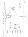
- a peak P 1 for FIG. 8 occurs in the dotted line corresponding to zero gold thickness. This peak represents the conventional wisdom that, at 850 nanometers, in the structure of FIG. 8, with no gold layer 155 present, the reflection coefficient attains a maximum at a wavelength of about 850 nanometers. The actual numerical value of the maximal reflection coefficient, at P 1 , is 0.998. (Numerical computations are not indicated.)
- Point P 2 is also consistent with conventional wisdom: when a gold layer of 50 angstroms is added to FIG. 8, the peak reflection coefficient, near point P 2 , falls below 0.99. The reflection coefficient falls further for a thicker gold layer of 100 angstroms in FIG. 8 (point P 3 ).
- points P 1 , P 2 , and P 3 indicate that, as progressively thicker layers of gold are added in the form of layer 155 in FIG. 8, starting with zero thickness for point P 1 , the reflection coefficient progressively drops in value.
- points P 2 and P 3 represent reflection coefficients which are considered non-usable.
- Point P 1 is non-usable because no layer of gold is present, and such a layer is required for another purpose in the invention, which is described below.
- FIG. 8 In pursuit of a sufficiently high reflection coefficient, the Inventors have discovered that, if the structure of FIG. 8 is modified in certain ways, then the reflection coefficient can be driven above the required minimum of 0.99. Modifications are shown in FIG. 9, and include (1) addition of the gold layer 155 of a specific thickness, (2) addition of the high-index layer 160 , adjacent the gold, and (3) insertion of elements (1) and (2) in the positions indicated.
- the Inventors begin with an ordinary mirror as in FIG. 8, with no gold layer 155 present. Then, as in FIG. 9, a high-index layer 160 , of one-quarter wave thickness, is added to the bottom of the mirror containing 10 layer-pairs, namely, PAIR 1 -PAIR 10 . Also, a layer of gold 155 , of proper thickness, is added adjacent the high-index layer 160 .
- the reflection coefficient is found to lie near point P 10 in FIG. 11 . (The reader is reminded that the solid plots in FIG. 11 correspond to FIG. 9.) When computed numerically, the reflection coefficient in this case is 0.9935. With a gold layer of zero thickness, the reflection coefficient is slightly higher, at 0.994, near point P 11 in FIG. 11 .
- the layer 155 of gold in FIG. 9 has an almost negligible effect on the reflection coefficient, if it is paired with the dielectric layer 160 .
- dielectric layer 160 is absent, and a gold layer is merely added to the structure of FIG. 8, then the situation is that of the points P 2 and P 3 in FIG. 11, wherein the gold layer renders the mirror unusable.
- one form of the invention employs the structure of FIG. 9 as the top mirror of FIG. 6 . That structure includes (1) the ten pairs, PAIR 1 -PAIR 10 , (2) the high-index titanium dioxide layer 160 , and (3) the gold layer 155 , in that order.
- FIG. 6 is a simplified schematic: the four layers of FIG. 6 indicating the top mirror actually represent the 22 layers in FIG. 9, which contain (1) the ten pairs, (2) layer 160 , and (3) the gold layer 155 .
- the gold layer 155 can be viewed as acting as part of the top mirror, or as acting as part of the gain region in FIG. 6 . These alternate views will be addressed later.
- the gold layer 100 in FIG. 6 provides another function, namely, it acts as a conductor for carrying current 106 from metal contact 109 to the p-type region 112 .
- a simplified process for fabricating the current blocking region 53 in FIG. 6 has been provided.
- Structures AA, BB, and CC in FIG. 12 are fabricated, using known techniques.
- the p-layer 112 in structure AA is fabricated, and then etched away, to produce the p-type mesa 112 in structure BB.
- the surrounding current-blocking regions 53 are fabricated, in structure CC.
- the gold layer 100 provides a current path for current 106 in FIG. 6 .
- the gold layer also cooperates with the layers of FIG. 9, to provide a sufficiently high reflection coefficient to support stimulated emission.
- FIG. 8 illustrates a prior-art structure.
- the reflection coefficient at interface 150 is indicated by point P 1 in FIG. 11 .
- the invention shifts that point P 1 to a point near point P 10 in FIG. 11, by utilizing the structure of FIG. 9, wherein the gold thickness is either 50 or 100 angstroms.
- P 10 in FIG. 11 is located at a wavelength which is different from 850 nanometers.
- the maximum reflectance, near P 10 now occurs at a longer wavelength: P 10 lies to the right of point P 1 in FIG. 11 .
- the maximum reflectance point has been shifted toward the red end of the optical spectrum.
- FIG. 13 shows the results of the stratagem.
- the solid lines in FIG. 13 are magnified versions of parts of the corresponding lines of FIG. 11 .
- the dashed lines in FIG. 13 indicate how the solid lines in that Figure are shifted when the stratagem is implemented.
- Arrows A 1 and A 2 indicate the shifting.
- the stratagem is to adjust the thickness of layer 160 in FIG. 9 by a correction factor.
- the correction factor is the quantity (1 ⁇ t Au /3000 A), wherein T Au is the thickness in Angstroms of the gold layer 155 .
- the correction factor is applied to layer 160 , to adjust its thickness.
- the correction factor in computing the correction factor, one divides the thickness, in Angstroms, of the gold layer 155 by 3,000, to obtain a quotient. Then one subtracts that quotient from unity. The result is a correction factor which is multiplied by the thickness of the quarter-wave layer 160 . The result is the actual thickness of layer 160 which is to be used. That layer 160 in FIG. 9 is deposited upon the gold layer 155 .
- the correction factor is (1 ⁇ 100/3,000), or 0.9667.
- the correction factor is (1 ⁇ 100/3,000), or 0.9667.
- the one-quarter-wave original thickness of layer 160 is determined by the wavelength of light within layer 160 , not in air or vacuum.
- the wavelength of light in a medium equals the free-space wavelength divided by the index of refraction of that material.
- the thickness of the gold layer 155 is a small fraction of the thickness of the quarter-wave layers.
- FIG. 13 indicates a wavelength of 850 nanometers, which corresponds to 850 ⁇ 10 ⁇ 9 meter.
- One hundred Angstroms corresponds to 100 ⁇ 10 ⁇ 10 meter.
- the thickness of the gold layer 155 corresponds to 10/850 of one wavelength, or roughly one percent (ie, 1/85) of a wavelength.
- the thickness of the gold layer 155 is roughly 3 percent (ie, 4/85) of a quarter wavelength.
- High-index layer 160 in FIG. 9 can be viewed as an extension of the resonant cavity, which is the region between the top mirror 103 in FIG. 6 and the bottom mirror 175 . It can be viewed as an extension of the resonant cavity because, traditionally, the cavity is viewed as terminating with a high-index material, and the mirror is viewed as beginning with a low-index material, namely layer LL in FIG. 6, which corresponds to the silicon dioxide layer in PAIR 1 in FIG. 9 .
- high-index layer 160 is a nominal quarter-wavelength in thickness, and is added to the thickness of the resonant cavity, which is an even number of quarter wavelengths, the cavity has now become an odd number of wavelengths in length.
- FIG. 14 illustrates the reflection coefficient of the entire prior-art structure: top mirror 33 , bottom mirror 34 , and the resonant cavity between them.
- N TOP increases from zero to 7
- the reflection coefficient drops. That is due to the fact that, as N TOP increases, the top mirror 33 becomes a better reflector.
- a Fabry-Perot cavity is being generated, explaining the drop in reflectivity.
- reflectance in FIG. 14 will equal zero: complete destructive interference will occur in the cavity.
- FIG. 15 illustrates the analogous reflectance for one form of the invention, namely, the structure of FIG. 6 using the mirror of FIG. 9 .
- the length of the cavity has been changed: it is now is an odd multiple of quarter wavelengths, at 3 quarter-wavelengths in this example. That is, the distance between the top mirror 103 in FIG. 6 and the bottom mirror 175 is 3 quarter wavelengths.
- Top layer 160 in FIG. 9 provides an additional quarter-wavelength (nominal) to make the cavity an even number of quarter wavelengths, namely, four.
- FIG. 15 indicates that, as the thickness of the gold layer increases, the wavelength at which minimal reflectance occurs increases. Another red shift has occurred.
- FIG. 16 illustrates a second stratagem for countering this red shift: the cavity (the distance between the top mirror 103 in FIG. 6 and the bottom mirror 175 ) is made 0.725 wavelengths in length, or slightly less than 0.75 wavelengths, which is 3 quarter-wavelengths.
- the gold layer 155 in FIG. 9 is 100 Angstroms thick.
- Layer 160 is the thickness computed according to the first stratagem, namely, 0.9667 ⁇ (one quarter wavelength).
- FIG. 17 illustrates a gain region 200 , the current blockers 205 , and mirrors 210 and 215 .
- Many of the components in, for example, FIG. 5 function to (1) hold the components of FIG. 17 in position and (2) deliver current to the gain region 200 . Those components have been eliminated from FIG. 17 .
- FIG. 18 illustrates one form of the invention.
- the components of FIG. 17 appear in FIG. 18, with the addition of gold film 155 and dielectric layer 160 .
- the triplet of the top mirror 215 , dielectric layer 160 , and the gold layer 155 are preferably positioned so that gold layer 155 lies against current blockers 53 .
- the current blockers 53 may be viewed as limiting the optical pathways taken by the photons reflected between the mirrors. Those pathways are limited to dashed box 220 . That is, the current blockers 53 surround part of the resonant cavity represented by dashed box 220 , and constrain the reflected light to travel through that region 222 .
- the gold layer 155 delivers current to the mesa (illustrated as mesa 112 in FIG. 12) which occupies region 222 in FIG. 18, and which lies in the paths within dashed box 220 .
- FIG. 7 illustrates an embodiment wherein the gold layer 300 is overlaid onto the p-layer mesa 305 .
- the top mirror 310 and the extra dielectric layer corresponding to layer 160 in FIG. 9 are deposited onto the gold layer 300 .
- the layers composing top mirror 310 and layer 160 are conformal with the gold layer 300 .
- the preceding discussion has been framed in the context of a film 155 constructed primarily of gold. However, other materials can be used, such as gold alloys. Other metals can be used, such as silver, copper, or any of the good conductors. Superconductors can be used, which are not necessarily classified as metals. Doped semiconductors of sufficiently high conductivity should not be ruled out, although they may form a PN junction with mesa 112 .
- the film 155 need not be of the single-crystal type.
- quarter-wave dielectric layer and similar terms are terms-of-art, and refer to a layer of dielectric material which is 1 ⁇ 4 wavelength in thickness. The wavelength is measured within the layer, not in free space.
Landscapes
- Physics & Mathematics (AREA)
- Condensed Matter Physics & Semiconductors (AREA)
- General Physics & Mathematics (AREA)
- Electromagnetism (AREA)
- Optics & Photonics (AREA)
- Semiconductor Lasers (AREA)
Abstract
Description
Claims (9)
Priority Applications (1)
| Application Number | Priority Date | Filing Date | Title |
|---|---|---|---|
| US09/873,640 US6707840B2 (en) | 2001-06-04 | 2001-06-04 | Vertical cavity surface emitting laser |
Applications Claiming Priority (1)
| Application Number | Priority Date | Filing Date | Title |
|---|---|---|---|
| US09/873,640 US6707840B2 (en) | 2001-06-04 | 2001-06-04 | Vertical cavity surface emitting laser |
Publications (2)
| Publication Number | Publication Date |
|---|---|
| US20020181530A1 US20020181530A1 (en) | 2002-12-05 |
| US6707840B2 true US6707840B2 (en) | 2004-03-16 |
Family
ID=25362032
Family Applications (1)
| Application Number | Title | Priority Date | Filing Date |
|---|---|---|---|
| US09/873,640 Expired - Fee Related US6707840B2 (en) | 2001-06-04 | 2001-06-04 | Vertical cavity surface emitting laser |
Country Status (1)
| Country | Link |
|---|---|
| US (1) | US6707840B2 (en) |
Cited By (2)
| Publication number | Priority date | Publication date | Assignee | Title |
|---|---|---|---|---|
| US20050133796A1 (en) * | 2003-12-23 | 2005-06-23 | Seo Jun H. | Nitride semiconductor light emitting diode and fabrication method thereof |
| US20090311521A1 (en) * | 2008-06-12 | 2009-12-17 | Anguel Nikolov | Thin film and optical interference filter incorporating high-index titanium dioxide and method for making them |
Families Citing this family (1)
| Publication number | Priority date | Publication date | Assignee | Title |
|---|---|---|---|---|
| CN119050809B (en) * | 2024-10-28 | 2025-02-07 | 南昌凯迅光电股份有限公司 | A red light VCSEL chip and its manufacturing method |
Citations (1)
| Publication number | Priority date | Publication date | Assignee | Title |
|---|---|---|---|---|
| US6144682A (en) * | 1998-10-29 | 2000-11-07 | Xerox Corporation | Spatial absorptive and phase shift filter layer to reduce modal reflectivity for higher order modes in a vertical cavity surface emitting laser |
-
2001
- 2001-06-04 US US09/873,640 patent/US6707840B2/en not_active Expired - Fee Related
Patent Citations (1)
| Publication number | Priority date | Publication date | Assignee | Title |
|---|---|---|---|---|
| US6144682A (en) * | 1998-10-29 | 2000-11-07 | Xerox Corporation | Spatial absorptive and phase shift filter layer to reduce modal reflectivity for higher order modes in a vertical cavity surface emitting laser |
Cited By (3)
| Publication number | Priority date | Publication date | Assignee | Title |
|---|---|---|---|---|
| US20050133796A1 (en) * | 2003-12-23 | 2005-06-23 | Seo Jun H. | Nitride semiconductor light emitting diode and fabrication method thereof |
| US7148514B2 (en) * | 2003-12-23 | 2006-12-12 | Samsung Electro-Mechanics Co., Ltd. | Nitride semiconductor light emitting diode and fabrication method thereof |
| US20090311521A1 (en) * | 2008-06-12 | 2009-12-17 | Anguel Nikolov | Thin film and optical interference filter incorporating high-index titanium dioxide and method for making them |
Also Published As
| Publication number | Publication date |
|---|---|
| US20020181530A1 (en) | 2002-12-05 |
Similar Documents
| Publication | Publication Date | Title |
|---|---|---|
| Hamaguchi et al. | A review on the latest progress of visible GaN-based VCSELs with lateral confinement by curved dielectric DBR reflector and boron ion implantation | |
| USRE41738E1 (en) | Red light laser | |
| CN102132466B (en) | Optoelectronic systems providing high-power high-brightness laser light based on field coupled arrays, linear arrays and stacks of semiconductor diode lasers | |
| US5498883A (en) | Superluminescent edge emitting device with apparent vertical light emission and method of making | |
| CN101467314B (en) | Surface-emitting semiconductor laser tube and manufacturing method thereof | |
| US5063569A (en) | Vertical-cavity surface-emitting laser with non-epitaxial multilayered dielectric reflectors located on both surfaces | |
| JPH02302085A (en) | Electric excitation cavity laser device | |
| US8270451B2 (en) | Edge emitting semiconductor laser having a phase structure | |
| US6819701B2 (en) | Super-luminescent folded cavity light emitting diode | |
| JPH06268330A (en) | Vcsel with horizontal index guide | |
| EP2675024B1 (en) | Electron beam pumped vertical cavity surface emitting laser | |
| JP2006210429A (en) | Surface emitting semiconductor laser | |
| US20110182317A1 (en) | Surface emitting semiconductor laser having a plurality of active zones | |
| CN103311805A (en) | Semiconductor stack and vertical cavity surface emitting laser | |
| US20070223549A1 (en) | High-Power Optoelectronic Device with Improved Beam Quality Incorporating A Lateral Mode Filtering Section | |
| CN112382924B (en) | Double-waveguide distributed feedback semiconductor laser and laser generation method | |
| JP2628801B2 (en) | Semiconductor laser structure | |
| US8175128B2 (en) | Semiconductor laser element and semiconductor laser device | |
| JPH0758418A (en) | Optoelectronic semiconductor device | |
| JP2884603B2 (en) | Semiconductor laser device | |
| US20240266802A1 (en) | Optoelectronic component and laser | |
| WO2021192672A1 (en) | Surface-emitting laser, surface-emitting laser array, electronic apparatus, and method for manufacturing surface-emitting laser | |
| RU2703922C2 (en) | Long-wave vertical-emitting laser with intracavity contacts | |
| US6707840B2 (en) | Vertical cavity surface emitting laser | |
| US5324964A (en) | Superluminescent surface light emitting device |
Legal Events
| Date | Code | Title | Description |
|---|---|---|---|
| FEPP | Fee payment procedure |
Free format text: PAT HOLDER NO LONGER CLAIMS SMALL ENTITY STATUS, ENTITY STATUS SET TO UNDISCOUNTED (ORIGINAL EVENT CODE: STOL); ENTITY STATUS OF PATENT OWNER: LARGE ENTITY |
|
| REFU | Refund |
Free format text: REFUND - SURCHARGE FOR LATE PAYMENT, SMALL ENTITY (ORIGINAL EVENT CODE: R2554); ENTITY STATUS OF PATENT OWNER: LARGE ENTITY Free format text: REFUND - SURCHARGE, PETITION TO ACCEPT PYMT AFTER EXP, UNINTENTIONAL (ORIGINAL EVENT CODE: R2551); ENTITY STATUS OF PATENT OWNER: LARGE ENTITY |
|
| AS | Assignment |
Owner name: CUBIC WAFER, INC., NEW HAMPSHIRE Free format text: CHANGE OF NAME;ASSIGNORS:XANOPTIX, INC.;XAN 3D TECHNOLOGIES;REEL/FRAME:019250/0609;SIGNING DATES FROM 20041019 TO 20050816 Owner name: XANOPTIX, INC., NEW HAMPSHIRE Free format text: ASSIGNMENT OF ASSIGNORS INTEREST;ASSIGNOR:ARALIGHT, INC.;REEL/FRAME:019250/0407 Effective date: 20031223 Owner name: ARALIGHT, INC., NEW JERSEY Free format text: ASSIGNMENT OF ASSIGNORS INTEREST;ASSIGNOR:GOOSSEN, KEITH W.;REEL/FRAME:019250/0347 Effective date: 20070430 |
|
| REMI | Maintenance fee reminder mailed | ||
| FPAY | Fee payment |
Year of fee payment: 4 |
|
| SULP | Surcharge for late payment | ||
| FEPP | Fee payment procedure |
Free format text: PAYOR NUMBER ASSIGNED (ORIGINAL EVENT CODE: ASPN); ENTITY STATUS OF PATENT OWNER: LARGE ENTITY |
|
| AS | Assignment |
Owner name: CUFER ASSET LTD. L.L.C., DELAWARE Free format text: ASSIGNMENT OF ASSIGNORS INTEREST;ASSIGNOR:CUBIC WAFER, INC.;REEL/FRAME:021433/0863 Effective date: 20080321 |
|
| FEPP | Fee payment procedure |
Free format text: PAYOR NUMBER ASSIGNED (ORIGINAL EVENT CODE: ASPN); ENTITY STATUS OF PATENT OWNER: LARGE ENTITY Free format text: PAYER NUMBER DE-ASSIGNED (ORIGINAL EVENT CODE: RMPN); ENTITY STATUS OF PATENT OWNER: LARGE ENTITY |
|
| FPAY | Fee payment |
Year of fee payment: 8 |
|
| REMI | Maintenance fee reminder mailed | ||
| LAPS | Lapse for failure to pay maintenance fees | ||
| STCH | Information on status: patent discontinuation |
Free format text: PATENT EXPIRED DUE TO NONPAYMENT OF MAINTENANCE FEES UNDER 37 CFR 1.362 |
|
| STCH | Information on status: patent discontinuation |
Free format text: PATENT EXPIRED DUE TO NONPAYMENT OF MAINTENANCE FEES UNDER 37 CFR 1.362 |
|
| FP | Lapsed due to failure to pay maintenance fee |
Effective date: 20160316 |